EP0476221A1 - Dispositif pour déterminer des points de coordonnées - Google Patents
Dispositif pour déterminer des points de coordonnées Download PDFInfo
- Publication number
- EP0476221A1 EP0476221A1 EP91105021A EP91105021A EP0476221A1 EP 0476221 A1 EP0476221 A1 EP 0476221A1 EP 91105021 A EP91105021 A EP 91105021A EP 91105021 A EP91105021 A EP 91105021A EP 0476221 A1 EP0476221 A1 EP 0476221A1
- Authority
- EP
- European Patent Office
- Prior art keywords
- cursor
- conductor pattern
- tablet
- power
- axis
- Prior art date
- Legal status (The legal status is an assumption and is not a legal conclusion. Google has not performed a legal analysis and makes no representation as to the accuracy of the status listed.)
- Granted
Links
Images




Classifications
-
- G—PHYSICS
- G06—COMPUTING OR CALCULATING; COUNTING
- G06F—ELECTRIC DIGITAL DATA PROCESSING
- G06F3/00—Input arrangements for transferring data to be processed into a form capable of being handled by the computer; Output arrangements for transferring data from processing unit to output unit, e.g. interface arrangements
- G06F3/01—Input arrangements or combined input and output arrangements for interaction between user and computer
- G06F3/03—Arrangements for converting the position or the displacement of a member into a coded form
- G06F3/041—Digitisers, e.g. for touch screens or touch pads, characterised by the transducing means
- G06F3/046—Digitisers, e.g. for touch screens or touch pads, characterised by the transducing means by electromagnetic means
Definitions
- the present invention relates to a device for determining position coordinates of a cursor on a tablet by detecting electromagnetic induction between the cursor coil and the grid-shaped conductors formed in the grid structures of the tablet, and in particular to a cordless type digitizer in which a cable for transmitting electric signals between the cursor and the tablet is eliminated.
- the cursor has a battery for supplying electric power to electric circuits in the cursor.
- An alternating current generated by these electric circuits flows in a cursor coil and generates an electromagnetic field on the tablet. This electromagnetic field induces electric voltages in the grid-shaped conductors in the grid structures.
- induced voltages in the grid-shaped conductors are processed in a processor to determine the position coordinates of the cursor on the tablet.
- an attribute (or attributes) of the point is sometimes necessary.
- an attribute of a point specifies a colour to display the coordinates of the point on a cathode ray tube display.
- this attribute is represented by the frequency of the alternating current in the cursor coil.
- a variety of tuning circuits must be provided in the cursor for generating a variety of frequencies, and in the signal processor for tuning to the frequencies.
- the primary object of this invention is to provide a cordless digitizer, in which the power-supply for the cursor is not a battery.
- the cursor of this invention is power-supplied by magnetic induction from the tablet.
- a tablet of a device for determining position coordinates there are two types of grid structures; in the one type, the length of the grid-shaped conductor pattern being in parallel to the Y-axis and the conductors being arranged along the X-axis for determining the position coordinate in the X-axis (hereafter will be called Y-directional conductor pattern), and in the other type, the length of the conductor pattern being in parallel to the X-axis and the conductors being arranged along the Y-axis for determining the position coordinate in the Y-axis (hereafter will be called X-directional conductor pattern).
- the Y-directional conductor pattern has polyphase spaced windings along the X-axis
- the X-directional conductor pattern has polyphase spaced windings along the Y-axis.
- the polyphase spaced windings of a X-directional conductor pattern can be excited by a polyphase alternating current for producing a uniform magnetic field on the table, and during the time when a X-directional conductor pattern is used for determining a position coordinate, the polyphase spaced windings of a Y-directional conductor pattern can be excited by the polyphase alternating current for producing the uniform magnetic field on the tablet.
- the cursor of this invention has a power-supply coupling coil in which an alternating-current voltage is induced by the uniform amplitude magnetic field on the tablet. This induced alternating-current voltage is rectified and smoothed to produce a direct-current voltage to be used as the power-supply for the cursor.
- Another object of this invention is to incorporate means for informing attribute data.
- the current in the cursor coil is modulated by code and this code is decoded in the signal processor to identify the attribute.
- Fig. 1 is a block diagram showing an embodiment of this invention, and 1 is a tablet, 21, 22, 23 are respectively signal frequency amplifiers, 3 is a 90° phase shifter for the signal frequency, 40 is a change-over switch, 5 is a signal processor, 6 is a power-supply oscillator, 61 is a 90° phase shifter for the power-supply frequency, and 62, 63 are respectively power-supply amplifiers.
- the cursor 1 (not shown in Fig. 1) which is to be placed on the tablet is shown in Fig. 2, where 101 is a cursor coil, 102 is a signal generator, 103 is an amplifier, 7 is a power-supply coupling coil, 8 is a rectifier, and 9 is a smoothing circuit.
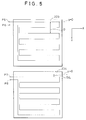
- Fig. 4 shows grid structures 201 and 202 of the tablet 2.
- the grid structures 201 and 202 have Y-directional conductor patterns in which the length of the conductor pattern is in parallel to the Y-axis.
- the pitch of the conductor pattern is D along the X-axis, and the spacing between the two conductor patterns on the grid structures 201 and 202 is D/4.
- the voltage induced between the terminals P1, P2 will be represented by Acos2 ⁇ (x/D) ⁇ sin ⁇ t.
- the coordinate position x of the cursor 1 is determined. Similarly, from the voltages induced in Y-directional conductor patterns which are shown in Fig. 5, the coordinate position y of the cursor 1 is determined.
- the windings from P1 to P2 and from P3 to P4 are used for coordinate determination
- the winding from P5 to P6 on the grid structure 203 is excited by the current from the amplifier 62
- the winding from P7 to P8 on the grid structure 204 is excited by the current from the amplifier 63.
- the current from the amplifier 62 is represented by Bsin ⁇ t
- that from the amplifier 63 is represented by Bcos ⁇ t, where ⁇ is the angular frequency of the power-supply voltage.
- Bcos2 ⁇ (y/D) ⁇ sin ⁇ t + Bcos2 ⁇ [(y-D/4)/D] ⁇ cos ⁇ t Bsin( ⁇ t + 2 ⁇ y/D)
- This magnetic field of uniform amplitude induces a constant amplitude voltage in the power-supply coupling coil 7 placed on the surface of the tablet 2.
- the induced voltage is rectified by the rectifier 8, smoothed by the smoothing circuit 9, and is supplied to the signal generator 102 arid the amplifier 103.
- a power-supply grid structure (or structures) must be supplemented in the tablet 2.
- the power-supply grid structure to be supplemented in the tablet 2 may consist of a power-supply grid structure of Y-directional conductor pattern as shown in Fig. 4 and a power-supply grid structure of X-directional conductor pattern as shown in Fig. 5.
- the power-supply grid structure of X-directional conductor pattern is to be used; and when X-directional conductor pattern is used for coordinate position determination, the power-supply grid structure of Y-directional conductor pattern is to be used.
- the interference between the power-supply frequency and the signal frequency can be easily avoided by frequency selective circuits, and one power-supply grid structure will be sufficient, when the power-supply frequency is not near to the signal frequency.
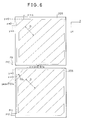
- Fig. 6 shows another embodiment of a power-supply grid structure.
- the conductor patterns 205 and 206 have 45° -directional conductor pattern which is oblique either to the X-axis or to the Y-axis.
- the pitch of the conductor is D in the 45° -direction, and the spacing of the two windings is D/4 as shown in Fig. 6, constituting a polyphased spacing.
- the signal voltage is modulated by a binary code.
- Fig. 3 is a block diagram of a cursor of this invention in which the signal voltage is modulated by a binary code.
- the same numerals in Fig. 3 indicate the same or the corresponding parts in Fig. 2, and 105 is a code generator and 106 is a modulator.
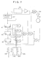
- FIG. 7 An embodiment of the code generator 105 and the modulator 106 is illustrated in Fig. 7.
- Fig. 7 the same numerals in Fig. 7 indicate the same or the corresponding parts in Fig. 3, and 107 is a frequency divider
- B1, B2, B3 are respectively binary counters
- G1, G2, G3, G4, G6, G8 are respectively AND gates
- G5, G7 are respectively OR gates.
- the AND gate G8 is the modulator 106 in Fig. 3.
- SW1, SW2, SW3, SW4 are respectively on-off switches.
- Fig. 8 shows voltage waveforms at points a, b, c, d, e, f in Fig. 7.
- the rectangular waveform at the point a which is shown by a in Fig. 7, is obtained by dividing the signal frequency of the oscillator 102. But this rectangular waveform voltage can be generated independently of the signal frequency.
- the voltage waveforms at points b, c, d in Fig. 7 will be as shown by b, c, d in Fig. 8.
- the gates G1, G2, G3, G4 pass the logic product of two signals b and c corresponding to the closed switch (or switches) of the four switches SW1, SW2, SW3, SW4.
- the output of the gate G6 is a logical product of the signal a, the signal d and the signal at the output of the gate G5. Therefore, when any one of the four switches SW1, SW2, SW3, SW4 is closed, the waveform at point e in Fig. 7 will be one of the four waveforms e1, e2, e3, e4 in Fig. 8.
- the front half of the waveform at the point f is used for determining position coordinates and also is used for frame synchronization of the waveform.
- Fig. 9 is a block diagram illustrating a decoder circuit provided in the signal processor 5 in an embodiment of this invention, and in Fig. 9, 110 is a detector, 111 is an amplifier, 112 is a phase detector, 113 is a low-pass filter, 114 is a voltage controlled oscillator, B1, B2, B3 are binary counters as B1, B2, B3 in Fig. 7, G9, G10, G11, G12 are AND gates respectively, M1, M2, M3, M4 are memories respectively, and 115 is a decoder.
- the closed circuit of the oscillator 114-B1-B2-B3-the phase detector112-the filter113-114 constitutes a phase lock loop, and the voltage controlled oscillator 114 generates a voltage having the waveform as shown a in Fig. 8, which is in phase with the output of the detector 110.
- the gates G9, G10, G11, G12 correspond to gates G1, G2, G3, G4 in Fig. 7 respectively, and the output of the binary counter B3, which corresponds to the signal d in Fig. 8 also controls these gates G9, G10, G11, G12. Therefore, each gate of these four gates selects corresponding signal from the four signals e1, e2, e3, e4 shown in Fig. 8, and stores the selected signal to a corresponding memory of the four memories M1, M2, M3, M4.
- the bit pattern in the memories M1 ⁇ M4 represents an on-off pattern of the switches SW1 ⁇ SW4 in Fig. 7, indicating the kind of the attribute set at the cursor.
- the decoder 115 decodes the 4 bit binary signal to 16 kinds of attributes.
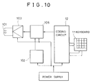
- Fig. 10 shows an example of a design of the code modulator shown by Fig. 7.
- the same numerals indicate the same or the corresponding parts in Fig. 3, and 11 is a keyboard, 12 is a coding circuit.
- the output of the coding circuit 12 corresponds to the output of G7 of Fig. 7.
- the modulation by the code is an amplitude modulation. But it is apparent that any other type of modulation may be used for this invention.
Landscapes
- Engineering & Computer Science (AREA)
- Physics & Mathematics (AREA)
- General Engineering & Computer Science (AREA)
- Theoretical Computer Science (AREA)
- Electromagnetism (AREA)
- Human Computer Interaction (AREA)
- General Physics & Mathematics (AREA)
- Position Input By Displaying (AREA)
- Measurement Of Length, Angles, Or The Like Using Electric Or Magnetic Means (AREA)
Applications Claiming Priority (6)
| Application Number | Priority Date | Filing Date | Title |
|---|---|---|---|
| JP25024190A JPH04130515A (ja) | 1990-09-21 | 1990-09-21 | 座標位置測定装置 |
| JP250241/90 | 1990-09-21 | ||
| JP254339/90 | 1990-09-26 | ||
| JP25433990A JP3029447B2 (ja) | 1990-09-26 | 1990-09-26 | 座標位置測定装置 |
| JP272185/90 | 1990-10-12 | ||
| JP2272185A JPH04148411A (ja) | 1990-10-12 | 1990-10-12 | 座標位置測定装置 |
Publications (2)
| Publication Number | Publication Date |
|---|---|
| EP0476221A1 true EP0476221A1 (fr) | 1992-03-25 |
| EP0476221B1 EP0476221B1 (fr) | 1995-12-20 |
Family
ID=27333919
Family Applications (1)
| Application Number | Title | Priority Date | Filing Date |
|---|---|---|---|
| EP91105021A Expired - Lifetime EP0476221B1 (fr) | 1990-09-21 | 1991-03-28 | Dispositif pour déterminer des points de coordonnées |
Country Status (3)
| Country | Link |
|---|---|
| US (1) | US5095180A (fr) |
| EP (1) | EP0476221B1 (fr) |
| DE (1) | DE69115613T2 (fr) |
Cited By (2)
| Publication number | Priority date | Publication date | Assignee | Title |
|---|---|---|---|---|
| DE19637869A1 (de) * | 1995-09-19 | 1997-03-20 | Japan System Dev Co | Analog-Digitalumsetzer mit einem elektronischen Stift, welcher den Auflagedruck erfaßt |
| EP1349055A3 (fr) * | 2002-02-05 | 2006-03-08 | Aiptek International Inc. | Configuration pour antennes multiples à boucles |
Families Citing this family (2)
| Publication number | Priority date | Publication date | Assignee | Title |
|---|---|---|---|---|
| US5345044A (en) * | 1991-04-29 | 1994-09-06 | Calcomp, Inc. | Cordless digitizer using electromagnetic locating signals |
| US7408838B1 (en) | 2007-01-22 | 2008-08-05 | Scale Master Technologies, Llc | Digitizing planimeter |
Citations (3)
| Publication number | Priority date | Publication date | Assignee | Title |
|---|---|---|---|---|
| US4786765A (en) * | 1986-07-23 | 1988-11-22 | Wacom Co., Ltd. | Coordinates input system |
| EP0307667A2 (fr) * | 1987-08-24 | 1989-03-22 | Wacom Company, Ltd. | Système pour l'entrée de coordonnées avec un crayon pour l'introduction des données |
| US4890096A (en) * | 1984-10-30 | 1989-12-26 | Wacom Co., Inc. | Coordinate input device with display |
Family Cites Families (4)
| Publication number | Priority date | Publication date | Assignee | Title |
|---|---|---|---|---|
| US4697059A (en) * | 1980-08-14 | 1987-09-29 | Sodick Co., Ltd. | Apparatus for pattern controlled electrode movement for E.D.M. |
| JPS6370326A (ja) * | 1986-09-12 | 1988-03-30 | Wacom Co Ltd | 位置検出装置 |
| JPS63298618A (ja) * | 1987-05-29 | 1988-12-06 | Graphtec Corp | ワイヤレス方式デジタイザ |
| KR0122737B1 (ko) * | 1987-12-25 | 1997-11-20 | 후루다 모또오 | 위치 검출 장치 |
-
1991
- 1991-03-13 US US07/668,781 patent/US5095180A/en not_active Expired - Lifetime
- 1991-03-28 DE DE69115613T patent/DE69115613T2/de not_active Expired - Fee Related
- 1991-03-28 EP EP91105021A patent/EP0476221B1/fr not_active Expired - Lifetime
Patent Citations (3)
| Publication number | Priority date | Publication date | Assignee | Title |
|---|---|---|---|---|
| US4890096A (en) * | 1984-10-30 | 1989-12-26 | Wacom Co., Inc. | Coordinate input device with display |
| US4786765A (en) * | 1986-07-23 | 1988-11-22 | Wacom Co., Ltd. | Coordinates input system |
| EP0307667A2 (fr) * | 1987-08-24 | 1989-03-22 | Wacom Company, Ltd. | Système pour l'entrée de coordonnées avec un crayon pour l'introduction des données |
Cited By (2)
| Publication number | Priority date | Publication date | Assignee | Title |
|---|---|---|---|---|
| DE19637869A1 (de) * | 1995-09-19 | 1997-03-20 | Japan System Dev Co | Analog-Digitalumsetzer mit einem elektronischen Stift, welcher den Auflagedruck erfaßt |
| EP1349055A3 (fr) * | 2002-02-05 | 2006-03-08 | Aiptek International Inc. | Configuration pour antennes multiples à boucles |
Also Published As
| Publication number | Publication date |
|---|---|
| DE69115613D1 (de) | 1996-02-01 |
| US5095180A (en) | 1992-03-10 |
| EP0476221B1 (fr) | 1995-12-20 |
| DE69115613T2 (de) | 1996-05-15 |
Similar Documents
| Publication | Publication Date | Title |
|---|---|---|
| EP0389963B1 (fr) | Dispositif pour déterminer les coordonnées de position de points sur une surface | |
| US5361029A (en) | System for locating multiple concealed underground objects | |
| EP0259841B1 (fr) | Appareil pour l'entrée de coordonnées | |
| US6239789B1 (en) | Position detecting method and apparatus for detecting a plurality of position indicators | |
| EP0254297B1 (fr) | Système d'entrée de coordonnées | |
| EP0607694A1 (fr) | Numériseur sans fil | |
| EP0737933A1 (fr) | Appareil de détection de position et dispositif de pointage | |
| US4552991A (en) | Absolute position coordinate determining device employing a single phase difference measurement to determine cursor position | |
| US4661656A (en) | Graphic tablet and method | |
| EP0476221B1 (fr) | Dispositif pour déterminer des points de coordonnées | |
| US5416280A (en) | Digitizer tablet using relative phase detection | |
| EP0549956A1 (fr) | Système de lecture de coordonnées pour détecter les états d'opération d'interrupteurs nombreux | |
| US20050280638A1 (en) | Position detecting device | |
| EP0388860B1 (fr) | Dispositif pour déterminer des coordonnées | |
| JP2608895B2 (ja) | 座標入力方法及びその装置 | |
| US11599220B2 (en) | Position detection apparatus configured to detect the positions of multiple position indicators, and position detection method | |
| JPH02292617A (ja) | 位置検出装置 | |
| US5313024A (en) | Coordinate reading system | |
| JPH03201018A (ja) | 位置検出装置及びそのセンス部 | |
| CN101865999A (zh) | 提高感应无线位置检测分辨率的方法 | |
| JP3029447B2 (ja) | 座標位置測定装置 | |
| JPH0629885A (ja) | 非接触通信システム | |
| JPH0756676A (ja) | 座標読取装置 | |
| JP2533218Y2 (ja) | 座標位置検出装置 | |
| JPS63115218A (ja) | 位置検出装置 |
Legal Events
| Date | Code | Title | Description |
|---|---|---|---|
| PUAI | Public reference made under article 153(3) epc to a published international application that has entered the european phase |
Free format text: ORIGINAL CODE: 0009012 |
|
| AK | Designated contracting states |
Kind code of ref document: A1 Designated state(s): CH DE GB IT LI |
|
| 17P | Request for examination filed |
Effective date: 19920506 |
|
| 17Q | First examination report despatched |
Effective date: 19950519 |
|
| RAP1 | Party data changed (applicant data changed or rights of an application transferred) |
Owner name: GRAPHTEC KABUSHIKI KAISHA |
|
| GRAA | (expected) grant |
Free format text: ORIGINAL CODE: 0009210 |
|
| AK | Designated contracting states |
Kind code of ref document: B1 Designated state(s): CH DE GB IT LI |
|
| REF | Corresponds to: |
Ref document number: 69115613 Country of ref document: DE Date of ref document: 19960201 |
|
| ITF | It: translation for a ep patent filed | ||
| PLBE | No opposition filed within time limit |
Free format text: ORIGINAL CODE: 0009261 |
|
| STAA | Information on the status of an ep patent application or granted ep patent |
Free format text: STATUS: NO OPPOSITION FILED WITHIN TIME LIMIT |
|
| 26N | No opposition filed | ||
| REG | Reference to a national code |
Ref country code: GB Ref legal event code: IF02 |
|
| PGFP | Annual fee paid to national office [announced via postgrant information from national office to epo] |
Ref country code: GB Payment date: 20030326 Year of fee payment: 13 |
|
| PGFP | Annual fee paid to national office [announced via postgrant information from national office to epo] |
Ref country code: CH Payment date: 20030331 Year of fee payment: 13 |
|
| PGFP | Annual fee paid to national office [announced via postgrant information from national office to epo] |
Ref country code: DE Payment date: 20030409 Year of fee payment: 13 |
|
| PG25 | Lapsed in a contracting state [announced via postgrant information from national office to epo] |
Ref country code: GB Free format text: LAPSE BECAUSE OF NON-PAYMENT OF DUE FEES Effective date: 20040328 |
|
| PG25 | Lapsed in a contracting state [announced via postgrant information from national office to epo] |
Ref country code: LI Free format text: LAPSE BECAUSE OF NON-PAYMENT OF DUE FEES Effective date: 20040331 Ref country code: CH Free format text: LAPSE BECAUSE OF NON-PAYMENT OF DUE FEES Effective date: 20040331 |
|
| PG25 | Lapsed in a contracting state [announced via postgrant information from national office to epo] |
Ref country code: DE Free format text: LAPSE BECAUSE OF NON-PAYMENT OF DUE FEES Effective date: 20041001 |
|
| GBPC | Gb: european patent ceased through non-payment of renewal fee |
Effective date: 20040328 |
|
| PG25 | Lapsed in a contracting state [announced via postgrant information from national office to epo] |
Ref country code: IT Free format text: LAPSE BECAUSE OF NON-PAYMENT OF DUE FEES Effective date: 20050328 |
|
| REG | Reference to a national code |
Ref country code: CH Ref legal event code: PL Ref country code: CH Ref legal event code: NV Representative=s name: BOVARD AG PATENTANWAELTE Ref country code: CH Ref legal event code: EP |