EP0489601A2 - Petit électrode en verre et procédé pour sa fabrication - Google Patents
Petit électrode en verre et procédé pour sa fabrication Download PDFInfo
- Publication number
- EP0489601A2 EP0489601A2 EP91311390A EP91311390A EP0489601A2 EP 0489601 A2 EP0489601 A2 EP 0489601A2 EP 91311390 A EP91311390 A EP 91311390A EP 91311390 A EP91311390 A EP 91311390A EP 0489601 A2 EP0489601 A2 EP 0489601A2
- Authority
- EP
- European Patent Office
- Prior art keywords
- glass
- substrate
- electrode
- electrolyte
- film
- Prior art date
- Legal status (The legal status is an assumption and is not a legal conclusion. Google has not performed a legal analysis and makes no representation as to the accuracy of the status listed.)
- Granted
Links
Images


Classifications
-
- G—PHYSICS
- G01—MEASURING; TESTING
- G01N—INVESTIGATING OR ANALYSING MATERIALS BY DETERMINING THEIR CHEMICAL OR PHYSICAL PROPERTIES
- G01N27/00—Investigating or analysing materials by the use of electric, electrochemical, or magnetic means
- G01N27/26—Investigating or analysing materials by the use of electric, electrochemical, or magnetic means by investigating electrochemical variables; by using electrolysis or electrophoresis
- G01N27/28—Electrolytic cell components
- G01N27/30—Electrodes, e.g. test electrodes; Half-cells
- G01N27/36—Glass electrodes
-
- G—PHYSICS
- G01—MEASURING; TESTING
- G01N—INVESTIGATING OR ANALYSING MATERIALS BY DETERMINING THEIR CHEMICAL OR PHYSICAL PROPERTIES
- G01N27/00—Investigating or analysing materials by the use of electric, electrochemical, or magnetic means
- G01N27/26—Investigating or analysing materials by the use of electric, electrochemical, or magnetic means by investigating electrochemical variables; by using electrolysis or electrophoresis
- G01N27/403—Cells and electrode assemblies
- G01N27/4035—Combination of a single ion-sensing electrode and a single reference electrode
Definitions
- the present invention relates to a small glass electrode and a process for the preparation thereof. More particularly, the present invention relates to a small glass electrode formed by utilizing a micro-machining technique and a process for the preparation thereof.
- a glass electrode is easily usable as a sensor for determining the hydrogen ion (H+) concentration in an aqueous solution, and is widely and generally used.
- the determination of the H+ concentration is required not only in ordinary chemical experiments but also in fermentation control and the medical field.
- a biosensor fabricated by combining a glass electrode with either enzymes or microorganisms can be used for determining various chemical compounds.
- glucose reacts with dissolved oxygen with the aid of a catalyst called glucose oxidase and is oxidized to gluconolactone. Changes of the H+ concentration during this reaction are measured, and the glucose concentration can be determined from the change quantities. According to a similar principle, the urea concentration can be determined.
- the H+ concentration is measured by utilizing the electroconductivity of glass. Namely, the phenomenon that when a glass film having a thickness of about 100 ⁇ m and an electric resistance of several hundred M ⁇ is placed in a solution, a voltage difference is produced according to the pH value of the solution is utilized.
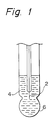
- Fig. 1 of the accompanying drawings illustrates the structure of a sensing portion of a conventional glass electrode, which comprises a reference electrode 2 composed of silver/silver chloride (Ag/AgCl), an internal solution 4 such as a potassium chloride (KCl) solution having a certain concentration, and a spherical sensing glass film 6 formed on the top end.
- a reference electrode 2 composed of silver/silver chloride (Ag/AgCl)
- an internal solution 4 such as a potassium chloride (KCl) solution having a certain concentration
- KCl potassium chloride
- the commercially available glass electrode has a size similar to that of a fountain pen, as shown in Fig. 1, and the glass electrode is formed by glazing and it is expensive.
- ISFET ion-sensitive electric field effect transistor
- the conventional glass electrode formed by glazing is large in size and is expensive.
- ISFET formed by the photolithography of an Si substrate insulation is indispensable and rise of the price is inevitably caused by the necessity of maintaining the insulation, and reduction of the price is not easy.
- a glass electrode which has a bonded structure comprising a reference electrode composed of silver/silver chloride, a glass substrate having a pad embedded therein, said pad being composed of gold or platinum and circuit-connected to the reference electrode, and a silicon substrate having a (100) plane selectively etched by the anisotroic etching technique and comprising a groove for injecting an electrolyte containing chlorine such as a potassium chloride buffer solution or hydrochloric acid solution, at least one hole for holding the electrolyte and a glass film formed in a portion corresponding to the reference electrode.
- an electrolyte containing chlorine such as a potassium chloride buffer solution or hydrochloric acid solution
- the glass film may have a multiple-layer (for example, two-layer) structure.
- a process for the preparation of a glass electrode which comprises a step of selectively etching a glass substrate and, forming a reference electrode composed of silver/silver chloride and a pad composed of gold or platinum and circuit-connected to the reference electrode, on the etched portion, a step of subjecting a silicon substrate having a (100) plane as the substrate face to anisotropic etching to form an electrolyte-injecting groove and at least one electrolyte-holding hole, a step of forming a glass film acting as a sensing film by utilizing a silicon oxide film used as the mask of said anisotropic etching, and a step of bonding the formed glass substrate and silicon substrate to each other.
- a process for the preparation of a glass electrode which comprises a step of selectively etching a glass substrate and forming a reference electrode composed of silver/silver chloride and a pad composed of gold or platinum and circuit-connected to the reference electrode, on the etched portion, a step of subjecting a silicon substrate having a (100) plane as the substrate face to anisotropic etching to form an electrolyte-injecting groove and at least one electrolyte-holding hole by using a patterned silicon oxide as a mask, a step of removing the silicon oxide film left on the silicon substrate face and forming a glass film acting as a sensing film in a lower portion of the holding hole, and a step of bonding the formed glass substrate and silicon substrate to each other.
- the process of the present invention may further comprise a step of injecting the electrolyte into the holding hole from the injecting groove according to need. Accordingly, a small glass electrode having an electrolyte injected in the holding hole is included within the scope of the present invention.
- the present invention enables a glass electrode having a small size to be provided.
- the present inventors already succeeded in providing a practically utilizable small Clark oxygen electrode by applying the micro-machining technique to an Si substrate (USP 4975175).
- This small oxygen electrode is often used for medical treatment.
- the oxygen concentration is measured relative to the H+ concentration, rather than the oxygen concentration alone.
- the glass substrate to be bonded to the Si substrate is required to adhere tightly to the Si substrate not only during the cooling course from the anode bonding treatment temperature, that is, about 250°C, to normal temperature but also in the application atmosphere.
- the glass substrate should have a thermal expansion coefficient approximate to that of Si
- the glass substrate should be composed of a glass having a low softening point
- the glass substrate should have a high resistance to thermal stress.
- Pyrex glass or lead glass is preferably used. This glass alone can be used as the substrate, or this glass can be used in a state bonded to other glass substrates or Si substrate.
- a glass electrode is formed by using the micro-machining technique according to the present invention.
- a thin glass film acting as the sensing film is formed by utilizing at least a part of an SiO2 film obtained by wet oxidation of a wafer.
- the thickness of the SiO2 film formed by the wet oxidation of the silicon wafer is about 1 ⁇ m at greatest, and it is impossible to increase the film thickness. Accordingly, in the process of the above-mentioned embodiment, a glass substrate is etched in advance to form a glass film having a desired thickness, a silicon oxide film left on the surface of the silicon substrate is removed, and then, the glass film is bonded to the bottom portion of the holding hole.
- the strength of the glass film acting as the sensing film is increased. Therefore, the yield is improved and the glass electrode can be used without breaking.
- the sensitivity to the H+ concentration is in practice sufficiently high.
- a glass electrode having a further enhanced sensitivity is desired, a glass electrode having a structure described below can be adopted.
- this equation is a theoretical formula, and it is not easy to construct the glass electrode so that the potential in accordance with this equation is obtained.
- the gradient coefficient -0.059 (-59 mV) of the Nernst equation is about -0.03 (-30 mV).
- the present invention improves the glass material.
- Lithium (Li) glass, sodium-calcium (Na-Ca) glass and the like are known as the glass for a glass electrode.
- these materials cannot be used as the sensing film for a small glass electrode. The reasons are as follows.
- the present invention it is sufficient if at least one holding hole is formed. However, if a plurality of holding holes are formed and glass films are bonded thereto, the risk of breaking the glass film is effectively reduced.
- bonding of the glass substrate and the silicon substrate is accomplished, for example, by a method of heating and bonding both substrates, a method using an adhesive or an anodic bonding method. From a practical viewpoint, the anode bonding method is preferably adopted.
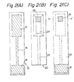
- Fig. 2(A) is a plane view showing a glass substrate 10 in the glass electrode according to one embodiment of the present invention
- Fig. 2(B) is a plane view showing an Si substrate 20 in the glass electrode according to this embodiment
- Fig. 2(C) is a plane view showing the glass electrode of one embodiment of the present invention, formed by reversing the glass substrate onto the Si substrate 20 and bonding them.
- a reference electrode 12 composed of Ag/AgCl, a lead-in line 14 composed of Au and a pad 16 composed of Au are embedded in the glass substrate 10.
- the substrate face of the Si substrate 20 is the (100) plane, and the Si substrate 20 is subjected to anisotropic etching, whereby a groove 22 for injecting an electrolyte, an electrolyte-holding hole 24 and a glass film 26 acting as the sensing film on at least a part of the hole 24 are formed.
- the groove only can also be made by the separate anisotropic etching.
- the broken line indicates an interior glass electrode-forming region, and the pad 16 and glass film 26 appear on the side of the Si substrate 20.
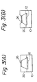
- Fig. 3(A) is a view showing the section taken along X-X′ in Fig. 2(C). As is seen from Fig. 3(A), the sensing film 26 is formed in the bottom portion of the etched Si substrate 20.
- Fig. 3(B) is a sectional view showing a modification of this Example 1, where the Si substrate is etched also from the bottom so that the sensing film 26 is formed slightly on the inner side of the Si substrate.
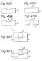
- Fig. 4 is a diagram illustrating the steps of preparing the glass electrode of the present invention. One embodiment of the preparation process will now be described with reference to Fig. 2 and Fig. 4.
- a negative photoresist is spin-coated on the surface of a Pyrex glass substrate (Iwaki 7740) having a diameter of 2 inches and a thickness of 500 ⁇ m and is heated and dried at 150°C for 30 minutes. Regions for formation of many reference electrodes 12, lead-in lines 14 and pads 16 are windowed and exposed by the photolithography, and the same resist is similarly coated and dried on the back surface.
- a Pyrex glass substrate Iwaki 7740
- the glass substrate is immersed in a mixed solution comprising 50% hydrofluoric acid (HF), concentrated nitric acid (HNO3) and ammonium fluoride [(NH4)F] at a ratio of 1/1/8 for 80 minutes to etch the glass substrate in a depth of 3 ⁇ m.
- HF hydrofluoric acid
- HNO3 concentrated nitric acid
- NH4F ammonium fluoride
- the resist is peeled by using a mixed solution comprising sulfuric acid (H2SO4) and hydrogen peroxide (H2O2) at a ratio of 2/1 [see Fig. 4(A)].
- the glass substrate 10 is sufficiently washed with a mixed solution of H2O2 and ammonia (NH4OH) and pure water, and is then dried.
- the thickness of the Cr film is 400 ⁇ and the thickness of the Au film is 4000 ⁇ .
- a positive resist film (DFRP-5000 supplied by Tokyo Oka) is spin-coated, and the resist is coated on regions for forming reference electrodes 12, lead-in lines 14 and pads 16 by the photolithography. Then, the Au film and Cr film are selectively etched to form a reference electrode pattern comprising reference electrodes 12, lead-in lines 14 and pads 16.
- the Au-etching solution is one formed by dissolving 4 g of KI and 1 g of I2 in 40 ml of water
- the Cr-etching solution is one formed by dissolving 0.5 g of NaOH and 1 g of K3Fe(CN)6 in 4 ml of water.
- silver (Ag) is vacuum-deposited on the portion for forming the reference electrode 12, and in the same manner as described above, coating of a positive resist, heat-drying, light exposure and development are carried out to coat the resist only on the reference electrode-forming portion. Then, Ag etching is conducted and the resist is dissolved and removed, whereby a silver film is formed on the reference electrode-forming portion.
- the Ag-etching solution is one comprising 29% NH4OH, 31% H2O2 and pure water at a ratio of 1/1/20.
- the entire substrate is sufficiently washed with pure water and immersed in a 0.1 M solution of FeCl3 for 10 minutes to form a thin AgCl layer on the surface of Ag.
- An Si substrate 20 having a (100) plane as the substrate face and having a thickness of 350 ⁇ m and a diameter of 2 inches is prepared, sufficiently washed with a mixed solution of H2O2 and NH4OH and pure water, and dried.
- the Si substrate 20 is subjected to wet oxidation at 1050°C for 200 minutes to form an SiO2 film 28 having a thickness of 1 ⁇ m on the entire surface.
- a negative resist (OMR-83 supplied by Tokyo Oka) having a viscosity of 60 cP is coated on the surface of the Si substrate, and light exposure, development and rinsing are carried out to form a resist pattern on the substrate. Then, the Si substrate 20 is immersed in a mixed solution comprising 50% HF and 40% NH4F at a ratio of 1/6 and the exposed portion of SiO2 is etched and removed to form a holding hole 24 [see Fig. 4(C)].
- the resist film is peeled in a mixed solution comprising sulfuric acid and hydrogen peroxide at a ratio of 2/1.
- the Si substrate 20 is immersed in 35% KOH at 80°C and anisotropic etching of silicon is carried out to form an electrolyte-holding hole 24 in the reference electrode portion.
- a glass film 26 acting as the sensing film is formed in the bottom portion of the holding hole 24 by utilizing an SiO2 film 28 having a thickness of 1 ⁇ m, formed by wet oxidation.
- SiO2 used as the mask is left on the surface of the Si substrate 20, a higher temperature is necessary for the anodic bonding. Therefore, SiO2 other than the glass film 26 is completely removed by the photolithography using a mixed solution comprising 50%HF and 40% NH4F at a ratio of 1/6. Thus, a vessel portion for storing an electrolyte is completed [see Fig. 4(D)].
- the so-prepared glass substrate 10 and Si substrate 20 are immersed in pure water, sufficiently washed under ultrasonic vibrations and dried, and both the substrates are bonded and a voltage of 1200 V is applied at a temperature of 250°C between the substrates so that the Si substrate 20 is located on the positive side and the glass substrate 10 is located on the negative side, whereby the anodic bonding of the glass substrate and the silicon substrate is effected [see Fig. 4(E)].
- an electrolyte is introduced into the interior of the electrode according to the following method.
- a beaker is charged with 0.1 M hydrochloric acid aqueous solution or an aqueous potassium chloride buffer solution contining a phosphoric acid (electrolyte), and the glass electrode is entirely immersed in the electrolyte and the entire system including the beaker is placed in a sealed vessel. Then, deaeration is carried out by a vacuum pump.
- the hole 22 for injecting the electrolyte 30 After bubbles have not come out of the hole 22 for injecting the electrolyte 30, air is introduced into the vessel.
- the hole can be filled with an epoxy regin.
- the electrolyte is introduced into the inner space of the electrode, whereby a small glass electrode is obtained [see Fig. 4(F)].
- a fine glass electrode can be prepared by using the micro-machining technique while maintaining a wafer-like shape. Accordingly, reduction of the cost is possible.
- the glass electrode can be stored in a dry state, long-period storage is possible.
- Fig. 5(A) is a plane view showing a glass substrate in the glass electrode according to another embodiment of the present invention
- Fig. 5(B) is a plane view showing an Si substrate in the glass electrode according to this embodiment
- Fig. 5(C) is a plane view showing the glass electrode of another embodiment of the present invention, formed by bonding the glass substrate and Si substrate shown in Figs. 5(A) and 5(B).
- Fig. 6 is a diagram illustrating the section taken along line X-X′ in Fig. 5(C).
- Fig. 7 is a diagram illustrating steps of forming the glass electrode according to another embodiment of the present invention.
- the glass substrate-forming step is the same as described in Example 1. Accordingly, the description is omitted.
- the Si substrate is prepared substantially in the same manner as described in Example 1, except that a part of the SiO2 film is not utilized as the glass film acting as the sensing film, but the SiO2 film is entirely removed.
- a Pyrex glass (Iwaki 7740) is etched in a mixed solution comprising 50% HF and concentrated HNO3 at a ratio of 2/1 to obtain a film having a thickness of about 50 ⁇ m, and the film is sufficiently washed to obtain a glass film 26 acting as the sensing film 26A.
- the glass film 26A is placed on the surface of the Si substrate 20 formed by perforating the Si substrate by the anisotropic etching and heated at 800°C to effect bonding [see Fig. 7(D)].
- the strength of the glass film of the formed glass electrode is increased and hence, the yield is increased, and the glass electrode is advantageous over the conventional glass electrode in that no breaking is caused during use.
- Fig. 8(A) is a plane view showing a glass substrate in the glass electrode according to still another embodiment of the present invention
- Fig. 8(B) is a plane view showing an Si substrate in the glass electrode according to this embodiment
- Fig. 8(C) is a plane view showing the glass electrode of still another embodiment of the present invention, formed by bonding the glass substrate and Si substrate shown in Figs. 8(A) and 8(B).
- Fig. 9 is a diagram illustrating the section taken along line X-X′ in Fig. 8(C).
- Fig. 10 is a diagram illustrating steps of forming the glass electrode according to still another embodiment of the present invention.
- the glass substrate-forming step is the same as described in Example 1. Accordingly, the description is omitted.
- the Si substrate is prepared substantially in the same manner as described in Example 1, except that a part of the SiO2 film is not utilized as the glass film acting as the sensing film, but the SiO2 film is entirely removed.
- a Pyrex glass (Iwaki 7740) is etched in a mixed solution comprising 50% HF and concentrated HNO3 at a ratio of 2/1 to obtain a film having a thickness of, for example, 20-150 ⁇ m, in this case 50 ⁇ m, and the film is sufficiently washed to obtain a first glass film 29A constituting a film 29A acting as the sensing film.
- the first glass film 29A is placed on the back surface of an Si substrate 20 having a perforated or piercing holding hole 24 formed by anisotropic etching of an Si substrate and heated at 750°C to effect bonding of the first glass film 29A to the Si substrate 20. Then, the Si substrate having the first glass film formed thereon is set at a sputtering device and an sodium-calcium Na-Ca glass is sputtered in a thickness of 500 nm to form a second glass film 29B on the first glass film 29A, whereby a glass film 26B acting as the sensing film is obtained [see Fig. 10(D)].
- the characteristics of the small glass electrode obtained in Example 3 are evaluated according to the following method.
- the evaluation is performed by monitoring changes of the potential of the glass electrode relative to the potential of an external reference electrode of silver/silver chloride by using an electrometer.
- the sensing portion of the electrode is immersed in a 10 mM TRIS (Trimethyl aminomethane) solution, and HCl is added to reduce the pH value.
- TRIS Trimethyl aminomethane
- a very clear response curve is obtained.
- the small glass electrode immediately shows a change and a 90% response time is 10 seconds.
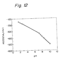
- a change of the electrode potential observed when the pH value is changed is shown in Fig. 12. It is seen that a linear relation is established between them over a broad pH value range of from 2 to 10.
- the gradient of the linear relation is a value approximate to -59 mV/pH of the theoretical value of the Nernst equation at 25°C.
Landscapes
- Chemical & Material Sciences (AREA)
- Life Sciences & Earth Sciences (AREA)
- Health & Medical Sciences (AREA)
- Biochemistry (AREA)
- Chemical Kinetics & Catalysis (AREA)
- Electrochemistry (AREA)
- Physics & Mathematics (AREA)
- Analytical Chemistry (AREA)
- Molecular Biology (AREA)
- General Health & Medical Sciences (AREA)
- General Physics & Mathematics (AREA)
- Immunology (AREA)
- Pathology (AREA)
- Pressure Sensors (AREA)
- Micromachines (AREA)
- Investigating Or Analyzing Materials By The Use Of Fluid Adsorption Or Reactions (AREA)
Applications Claiming Priority (4)
| Application Number | Priority Date | Filing Date | Title |
|---|---|---|---|
| JP400550/90 | 1990-12-06 | ||
| JP2400550A JPH04213048A (ja) | 1990-12-06 | 1990-12-06 | 小型ガラス電極とその製造方法 |
| JP3164750A JPH0510916A (ja) | 1991-07-05 | 1991-07-05 | 小型ガラス電極 |
| JP164750/91 | 1991-07-05 |
Publications (3)
| Publication Number | Publication Date |
|---|---|
| EP0489601A2 true EP0489601A2 (fr) | 1992-06-10 |
| EP0489601A3 EP0489601A3 (en) | 1994-09-21 |
| EP0489601B1 EP0489601B1 (fr) | 1997-11-05 |
Family
ID=26489741
Family Applications (1)
| Application Number | Title | Priority Date | Filing Date |
|---|---|---|---|
| EP91311390A Expired - Lifetime EP0489601B1 (fr) | 1990-12-06 | 1991-12-06 | Petite électrode en verre et procédé pour sa fabrication |
Country Status (4)
| Country | Link |
|---|---|
| US (2) | US5417837A (fr) |
| EP (1) | EP0489601B1 (fr) |
| KR (1) | KR960010690B1 (fr) |
| DE (1) | DE69128128T2 (fr) |
Cited By (1)
| Publication number | Priority date | Publication date | Assignee | Title |
|---|---|---|---|---|
| WO1998021572A1 (fr) * | 1996-11-15 | 1998-05-22 | Rosemount Analytical Inc. | Detecteur tecsi a entree gardee, monte sur face dorsale de substrat |
Families Citing this family (9)
| Publication number | Priority date | Publication date | Assignee | Title |
|---|---|---|---|---|
| US5837113A (en) * | 1990-12-06 | 1998-11-17 | Fujitsu Limited | Small glass electrode |
| US5716535A (en) * | 1996-03-05 | 1998-02-10 | Micron Technology, Inc. | Methods and etchants for etching oxides of silicon with low selectivity |
| US7070590B1 (en) * | 1996-07-02 | 2006-07-04 | Massachusetts Institute Of Technology | Microchip drug delivery devices |
| IL133453A0 (en) * | 1999-12-10 | 2001-04-30 | Shellcase Ltd | Methods for producing packaged integrated circuit devices and packaged integrated circuit devices produced thereby |
| US20030168431A1 (en) * | 2002-02-25 | 2003-09-11 | Ritdisplay Corporation | Etchant composition for silver alloy |
| US7033664B2 (en) | 2002-10-22 | 2006-04-25 | Tessera Technologies Hungary Kft | Methods for producing packaged integrated circuit devices and packaged integrated circuit devices produced thereby |
| US8728289B2 (en) | 2005-12-15 | 2014-05-20 | Medtronic, Inc. | Monolithic electrodes and pH transducers |
| MY150721A (en) * | 2009-10-24 | 2014-02-28 | Mimos Berhad | Method of fabricating integrated reference electrode |
| RU2762516C1 (ru) * | 2021-02-12 | 2021-12-21 | Олег Александрович Поваляев | Измерительный модуль |
Family Cites Families (18)
| Publication number | Priority date | Publication date | Assignee | Title |
|---|---|---|---|---|
| US2366489A (en) * | 1940-08-02 | 1945-01-02 | Nat Technical Lab | Glass electrode and method |
| US3458422A (en) * | 1966-08-08 | 1969-07-29 | Leeds & Northrup Co | Laminated glass electrode diaphragm |
| US3560256A (en) * | 1966-10-06 | 1971-02-02 | Western Electric Co | Combined thick and thin film circuits |
| US3573948A (en) * | 1968-01-29 | 1971-04-06 | Ppg Industries Inc | Methods of making an image plane plate |
| US3676319A (en) * | 1969-03-28 | 1972-07-11 | Radiometer As | Electrode, half cell and electrode component for the measurement of electromotive force |
| US3676391A (en) * | 1970-04-03 | 1972-07-11 | Dexter Corp | Coating compositions for polyolefin substrates |
| US4282079A (en) * | 1980-02-13 | 1981-08-04 | Eastman Kodak Company | Planar glass ion-selective electrode |
| JPS58180936A (ja) * | 1982-04-17 | 1983-10-22 | Fuigaro Giken Kk | 燃焼状態検出素子およびその製造方法 |
| US4592824A (en) * | 1985-09-13 | 1986-06-03 | Centre Suisse D'electronique Et De Microtechnique S.A. | Miniature liquid junction reference electrode and an integrated solid state electrochemical sensor including the same |
| EP0231033B1 (fr) * | 1986-01-31 | 1991-01-02 | Fuji Photo Film Co., Ltd. | Procédé pour mesurer l'activité ionique |
| DE3770507D1 (de) * | 1986-03-31 | 1991-07-11 | Hitachi Chemical Co Ltd | Verfahren zur metallisierung von glasoberflaechen. |
| DE3789491T2 (de) * | 1986-11-27 | 1994-10-20 | Horiba Ltd | Plattenförmige Glaselektrode. |
| DE3875149T2 (de) * | 1987-03-27 | 1993-02-11 | Fujitsu Ltd | Miniaturisierter biofuehler mit miniaturisierter sauerstoffelektrode sowie sein herstellungsverfahren. |
| US4786396A (en) * | 1987-06-26 | 1988-11-22 | The Washington Technology Center | Ion electrode and method of making it |
| US4874499A (en) * | 1988-05-23 | 1989-10-17 | Massachusetts Institute Of Technology | Electrochemical microsensors and method of making such sensors |
| US4863560A (en) * | 1988-08-22 | 1989-09-05 | Xerox Corp | Fabrication of silicon structures by single side, multiple step etching process |
| DE3921528A1 (de) * | 1989-06-30 | 1991-01-10 | Draegerwerk Ag | Messzelle fuer den elektrochemischen gasnachweis |
| US5160361A (en) * | 1990-06-13 | 1992-11-03 | Matsushita Electric Industrial Co., Ltd. | Method of manufacturing optical element |
-
1991
- 1991-12-06 DE DE69128128T patent/DE69128128T2/de not_active Expired - Fee Related
- 1991-12-06 EP EP91311390A patent/EP0489601B1/fr not_active Expired - Lifetime
- 1991-12-06 KR KR1019910022316A patent/KR960010690B1/ko not_active Expired - Fee Related
- 1991-12-06 US US07/803,433 patent/US5417837A/en not_active Expired - Fee Related
-
1995
- 1995-06-05 US US08/463,925 patent/US5660741A/en not_active Expired - Fee Related
Cited By (2)
| Publication number | Priority date | Publication date | Assignee | Title |
|---|---|---|---|---|
| WO1998021572A1 (fr) * | 1996-11-15 | 1998-05-22 | Rosemount Analytical Inc. | Detecteur tecsi a entree gardee, monte sur face dorsale de substrat |
| US5833824A (en) * | 1996-11-15 | 1998-11-10 | Rosemount Analytical Inc. | Dorsal substrate guarded ISFET sensor |
Also Published As
| Publication number | Publication date |
|---|---|
| US5660741A (en) | 1997-08-26 |
| US5417837A (en) | 1995-05-23 |
| EP0489601A3 (en) | 1994-09-21 |
| KR960010690B1 (ko) | 1996-08-07 |
| EP0489601B1 (fr) | 1997-11-05 |
| DE69128128D1 (de) | 1997-12-11 |
| DE69128128T2 (de) | 1998-03-05 |
Similar Documents
| Publication | Publication Date | Title |
|---|---|---|
| KR960012335B1 (ko) | 산소전극 | |
| US5431806A (en) | Oxygen electrode and temperature sensor | |
| US5747669A (en) | Oxygen electrode and its manufacture | |
| EP0489601B1 (fr) | Petite électrode en verre et procédé pour sa fabrication | |
| Steinkuhl et al. | Micromachined glucose sensor | |
| US5837113A (en) | Small glass electrode | |
| JP2838901B2 (ja) | 小型酸素電極及びその製造方法 | |
| Suzuki et al. | Development of a miniature Clark-type oxygen electrode using semiconductor techniques and its improvement for practical applications | |
| JP2844381B2 (ja) | 酸素電極及びその製造方法 | |
| JPS63238548A (ja) | 酸素電極 | |
| JP2743535B2 (ja) | 集積型センサとその製造方法 | |
| JPH0584860B2 (fr) | ||
| JPH02236154A (ja) | 小型酸素電極の製造法 | |
| JP2530689B2 (ja) | 小型酸素電極 | |
| JPH04213048A (ja) | 小型ガラス電極とその製造方法 | |
| JP2767868B2 (ja) | 小型酸素電極 | |
| Hiratsuka et al. | A Self‐Contained Glucose Sensor Chip with Arrayed Capillaries | |
| JPH0599883A (ja) | 小型ガラス電極 | |
| JPH0510916A (ja) | 小型ガラス電極 | |
| JP2661240B2 (ja) | 小型l―リジンセンサとその製造方法 | |
| JP2530690B2 (ja) | 小型酸素電極 | |
| JP2943281B2 (ja) | 小型酸素電極とその製造方法 | |
| JPH09182738A (ja) | 酸素電極およびその製造方法 | |
| JPH0375552A (ja) | 酵素電極 | |
| JPH06281617A (ja) | 小型ガラス電極およびその製法 |
Legal Events
| Date | Code | Title | Description |
|---|---|---|---|
| PUAI | Public reference made under article 153(3) epc to a published international application that has entered the european phase |
Free format text: ORIGINAL CODE: 0009012 |
|
| AK | Designated contracting states |
Kind code of ref document: A2 Designated state(s): CH DE FR GB LI |
|
| PUAL | Search report despatched |
Free format text: ORIGINAL CODE: 0009013 |
|
| AK | Designated contracting states |
Kind code of ref document: A3 Designated state(s): CH DE FR GB LI |
|
| 17P | Request for examination filed |
Effective date: 19950314 |
|
| 17Q | First examination report despatched |
Effective date: 19960306 |
|
| GRAG | Despatch of communication of intention to grant |
Free format text: ORIGINAL CODE: EPIDOS AGRA |
|
| GRAH | Despatch of communication of intention to grant a patent |
Free format text: ORIGINAL CODE: EPIDOS IGRA |
|
| GRAH | Despatch of communication of intention to grant a patent |
Free format text: ORIGINAL CODE: EPIDOS IGRA |
|
| GRAA | (expected) grant |
Free format text: ORIGINAL CODE: 0009210 |
|
| AK | Designated contracting states |
Kind code of ref document: B1 Designated state(s): CH DE FR GB LI |
|
| PG25 | Lapsed in a contracting state [announced via postgrant information from national office to epo] |
Ref country code: LI Free format text: LAPSE BECAUSE OF FAILURE TO SUBMIT A TRANSLATION OF THE DESCRIPTION OR TO PAY THE FEE WITHIN THE PRESCRIBED TIME-LIMIT Effective date: 19971105 Ref country code: CH Free format text: LAPSE BECAUSE OF FAILURE TO SUBMIT A TRANSLATION OF THE DESCRIPTION OR TO PAY THE FEE WITHIN THE PRESCRIBED TIME-LIMIT Effective date: 19971105 |
|
| REG | Reference to a national code |
Ref country code: CH Ref legal event code: EP |
|
| REF | Corresponds to: |
Ref document number: 69128128 Country of ref document: DE Date of ref document: 19971211 |
|
| ET | Fr: translation filed | ||
| REG | Reference to a national code |
Ref country code: CH Ref legal event code: PL |
|
| PLBE | No opposition filed within time limit |
Free format text: ORIGINAL CODE: 0009261 |
|
| STAA | Information on the status of an ep patent application or granted ep patent |
Free format text: STATUS: NO OPPOSITION FILED WITHIN TIME LIMIT |
|
| 26N | No opposition filed | ||
| REG | Reference to a national code |
Ref country code: GB Ref legal event code: IF02 |
|
| PGFP | Annual fee paid to national office [announced via postgrant information from national office to epo] |
Ref country code: GB Payment date: 20051130 Year of fee payment: 15 |
|
| PGFP | Annual fee paid to national office [announced via postgrant information from national office to epo] |
Ref country code: DE Payment date: 20051201 Year of fee payment: 15 |
|
| PGFP | Annual fee paid to national office [announced via postgrant information from national office to epo] |
Ref country code: FR Payment date: 20051208 Year of fee payment: 15 |
|
| PG25 | Lapsed in a contracting state [announced via postgrant information from national office to epo] |
Ref country code: DE Free format text: LAPSE BECAUSE OF NON-PAYMENT OF DUE FEES Effective date: 20070703 |
|
| GBPC | Gb: european patent ceased through non-payment of renewal fee |
Effective date: 20061206 |
|
| REG | Reference to a national code |
Ref country code: FR Ref legal event code: ST Effective date: 20070831 |
|
| PG25 | Lapsed in a contracting state [announced via postgrant information from national office to epo] |
Ref country code: GB Free format text: LAPSE BECAUSE OF NON-PAYMENT OF DUE FEES Effective date: 20061206 |
|
| PG25 | Lapsed in a contracting state [announced via postgrant information from national office to epo] |
Ref country code: FR Free format text: LAPSE BECAUSE OF NON-PAYMENT OF DUE FEES Effective date: 20070102 |