EP0497441A2 - Verbessertes synchronisches Taktsystem für Mikroprozessor - Google Patents
Verbessertes synchronisches Taktsystem für Mikroprozessor Download PDFInfo
- Publication number
- EP0497441A2 EP0497441A2 EP92300018A EP92300018A EP0497441A2 EP 0497441 A2 EP0497441 A2 EP 0497441A2 EP 92300018 A EP92300018 A EP 92300018A EP 92300018 A EP92300018 A EP 92300018A EP 0497441 A2 EP0497441 A2 EP 0497441A2
- Authority
- EP
- European Patent Office
- Prior art keywords
- timing
- bus
- clock
- coupled
- timing clock
- Prior art date
- Legal status (The legal status is an assumption and is not a legal conclusion. Google has not performed a legal analysis and makes no representation as to the accuracy of the status listed.)
- Granted
Links
Images


Classifications
-
- G—PHYSICS
- G06—COMPUTING OR CALCULATING; COUNTING
- G06F—ELECTRIC DIGITAL DATA PROCESSING
- G06F1/00—Details not covered by groups G06F3/00 - G06F13/00 and G06F21/00
- G06F1/04—Generating or distributing clock signals or signals derived directly therefrom
-
- G—PHYSICS
- G06—COMPUTING OR CALCULATING; COUNTING
- G06F—ELECTRIC DIGITAL DATA PROCESSING
- G06F13/00—Interconnection of, or transfer of information or other signals between, memories, input/output devices or central processing units
- G06F13/38—Information transfer, e.g. on bus
- G06F13/42—Bus transfer protocol, e.g. handshake; Synchronisation
- G06F13/4204—Bus transfer protocol, e.g. handshake; Synchronisation on a parallel bus
- G06F13/4208—Bus transfer protocol, e.g. handshake; Synchronisation on a parallel bus being a system bus, e.g. VME bus, Futurebus, Multibus
- G06F13/4217—Bus transfer protocol, e.g. handshake; Synchronisation on a parallel bus being a system bus, e.g. VME bus, Futurebus, Multibus with synchronous protocol
Definitions
- the present invention generally relates to a timing system for use in a microprocessor for initiating microprocessor outputs onto and input sampling from an external bus in synchronism with a bus timing clock on the bus.
- the present invention more particularly relates to such a timing system which is configurable for providing the external bus with the bus timing clock or being driven by an externally generated bus timing clock.
- the timing system of the present invention is configured to provide the bus with the bus timing clock and when so configured, is also arranged to minimize the time required to provide an output onto the bus (clock to output time).
- the timing system is also configured to be readily driven by an externally generated bus timing clock.
- Processing systems which incorporate at least one processor and at least one device, such as a memory, external to the microprocessor generally include an external bus to permit the microprocessor to perform external accesses.
- external accesses When such external accesses are required, such as when the microprocessor provides an output onto the external bus or samples an input from the external bus, the external accesses must be performed by the microprocessor in synchronism with the bus timing clock which controls the timing of the external bus.
- the bus timing clock may or may not be at the same frequency as the microprocessor timing clocks and, in either case, is generally not in phase with the microprocessor timing clocks.
- the external bus timing generally only permits microprocessor outputs onto the external bus when the bus clock is in a predetermined portion of its cycle, such as when the bus clock is at a high level, and only permits input sampling from the external bus when the external bus timing clock is in another predetermined portion of its clock cycle, such as when the bus timing clock is at a low level.
- microprocessors generally require a timing system for synchronizing external bus accesses with the bus timing clock which controls the timing of the external bus.
- the synchronizing timing depends on the occurrence of the rising edges of the bus timing clock.
- the external bus Upon a rising edge of the bus timing clock, the external bus is ready to receive outputs, such as data, from the microprocessor.
- the time required for the microprocessor to provide an output from the rising edge of the bus timing clock is referred to as the clock to output time and is an important parameter since, as the clock to output time is shortened, the time that the external system has for sampling the microprocessor outputs is lengthened. Also of importance is the set-up time which is the time from when an input to be sampled by the microprocessor is provided by the external bus to the next rising edge of the bus timing clock.
- a shortened set-up time gives the external system more time to sample a responsive output from the microprocessor, such as when the microprocessor must change the state of the bus during the next bus timing clock cycle.
- Microprocessors are also often required to generate the bus timing clock for the external bus and the external system in addition to generating its own internal timing clocks.
- the timing system of one known microprocessor is adapted to be coupled to an external clock source having a frequency twice that of the bus timing clock and the microprocessor internal timing clocks.
- the timing system uses the external clock to derive an intermediate clock from which it generates the bus timing clock.
- the bus timing clock is then used to generate the internal microprocessor timing clocks. While this configuration is satisfactory, the clock to output time is lengthened since the rising edges of the internal microprocessor clock controlling outputs is necessarily delayed with respect to the rising edges of the bus timing clock.
- the timing systems of microprocessors are also called upon to be driven by an externally generated bus timing clock, as for example in multiprocessor systems.
- the aforementioned prior art processor still generates its own internal timing clocks in response to the externally generated bus timing clock.
- the implementation of this system leaves much to be desired. For example, required internal duty cycles, to satisfy microprocessor speed path requirements, must be met. This problem is aggravated by the requirement that the externally generated bus timing clock be a CMOS input requiring TTL (transistor-transistor logic) level translation which skews the duty cycles from which the microprocessor internal timing clocks are derived. This makes it difficult for duty cycle requirements of the internal microprocessor timing clocks to be met for high frequency microprocessor operation.
- timing system for use in a microprocessor for synchronizing microprocessor external accesses to the bus timing clock of an external bus.
- a timing system should be configured to be readily implemented to be driven by an externally generated bus timing clock.
- Such a timing system should be further configured for providing the external bus with the bus timing clock and, when so configured, should additionally be capable of reducing the clock to output times.
- the present specification describes a timing system for use in a microprocessor for synchronizing microprocessor outputs onto an external bus with the bus timing clock on the external bus.
- the timing system is adapted to be coupled to an external clock source and includes buffer means including an input adapted to be coupled to the external clock source for generating an intermediate clock in response to the external clock source, first generating means coupled to the buffer means for generating first and second microprocessor timing clocks responsive to the intermediate clock with the first and second timing clock being of inverse phase relation and second generating means coupled to the buffer means and adapted to be coupled to the external bus for providing the external bus with the bus timing clock responsive to the intermediate clock.
- the second and first generating means are arranged such that the rising edges of the bus timing clock substantially coincide with the rising edges of the first timing clock and the falling edges of the second timing clock.
- the timing system further includes output means coupled to the first and second generating means and adapted to be coupled to the external bus for initiating a microprocessor output onto the external bus upon the common assertion of the bus timing clock and the first timing clock.
- the timing system may also include input means adapted to be coupled to the external bus and coupled to the first and second generating means for initiating the reception of an input from the external bus upon inverse assertion of the bus timing clock and the second timing clock.
- the present specification further describes a timing system for use in a microprocessor for synchronizing microprocessor external bus outputs with a bus timing clock.
- the timing system provides improved flexibility by being configured for either generating the bus timing clock when in a first mode of operation or being driven by an externally generated bus timing clock when in a second mode of operation.
- the timing system includes buffer means having an input adapted to be coupled to an external clock source for generating a first intermediate clock when said timing system is operable in said first mode or coupled to an externally generated bus timing clock for generating a second intermediate clock when the timing system is operable in the second mode and first generating means coupled to the buffer means for generating first and second microprocessor timing clocks in response to the first intermediate clock when the timing system is in the first mode and in response to the second intermediate clock when the timing system is in the second mode.
- the first and second timing clocks are opposite in phase relation.
- the timing system further includes second generating means coupled to the buffer means when said timing system is in the first mode for internally generating the bus timing clock in response to the first intermediate clock.
- the second generating means also includes an output adapted to be coupled to the bus for providing the bus with the internally generated bus timing clock when the timing system is in the first mode and also being adapted to be coupled to the bus when the timing system is in the second mode for receiving the externally generated bus timing clock.
- the timing system further includes enable means responsive to a select signal for coupling the second generating means to the buffer means when the timing system is in the first mode and decoupling the second generating from the buffer means when the timing system is in the second mode and output means coupled to the first generating means for receiving the first timing clock and coupled to the second generating means output for receiving the internally generated bus timing clock when the timing system is in the first mode or the externally generated bus timing clock when the timing system is in the second mode.
- the output means is also coupled to the bus and is arranged to initiate an output onto the bus upon the common assertion of the first timing clock and the internally generated bus timing clock when the timing system is in the first mode or upon the common assertion of the first timing clock and the externally generated bus timing clock when the timing system is in the second mode.
- the timing system 10 generally includes a buffer 12, first generating means 14, second generating means 16, output means 18, input means 20, and enable means 22.
- the timing system 10 is preferably implemented within the integrated circuit of the microprocessor and is thus preferably implemented using CMOS technology.
- the buffer 12 includes an input 24 which is coupled to an external input pin 26 of the integrated circuit.
- the timing system 10 is configured for operation in a first mode wherein the timing system provides an external bus with its bus timing clock in response to an external clock source being coupled to the input pin 26 and operative in a second mode of operation wherein the timing system 10 is driven by an externally generated bus timing clock which is coupled to the input pin 26.
- the buffer 12 has an output 28 which is coupled to the first generating means 14.
- the buffer 12 When the timing system is in the first mode of operation, the buffer 12 provides at its output 28 a first intermediate clock in response to the external clock source coupled to input pin 26 and when the timing system is operative in the second mode of operation, the buffer 12 provides at its output 28 a second intermediate clock in response to the externally generated bus timing clock coupled to input pin 26.
- the intermediate clocks are utilized by the first generating means 14 for providing at outputs 30 and 32 first and second microprocessor timing clocks PH1 and PH2 respectively.
- the buffer 12 buffers the input clocks that it receives and provides TTL translation when the input clock to buffer 12 is an externally generated bus timing clock.
- the buffer 12 provides duty cycle adjustments to accommodate speed paths within the microprocessor.
- the buffer 12, in practicing the present invention is a self-regulating clock generator of the type fully described in co-pending U.S. Patent Application Serial No. , filed June 1, 1990, in the names of David B. Witt and Brian D. McMinn entitled SELF-REGULATING CLACK GENERATOR, which application is assigned to the assignee of the present invention and which is incorporated herein by reference.
- the first generating means 14 responsive to the intermediate clocks provided by the buffer 12 at output 28, generates at outputs 30 and 32 first and second microprocessor timing clocks PH1 and PH2 respectively which are of inverse phase relation.
- the first generating means includes a first NOR gate 34, a first plurality of buffering inverters 36, 38, 40 and 42, a second NOR gate 44, a second plurality of buffering inverters 46, 48, 50 and 52, and another inverter 54.
- the first plurality of inverters, 36, 38, 40 and 42 are coupled between the output of NOR gate 34 and the output 30 of the first generating means.
- the second plurality of buffering inverters, 46, 48 50 and 52 are similarly coupled between the output of NOR gate 44 and the output 32 of the first generating means 14.
- NOR gate 44 has an input coupled directly to the output 28 of buffer 12 and
- NOR gate 34 has an input which is coupled to the output 28 of buffer 12 through the inverter 54.
- the NOR gates 34 and 44 each have their outputs and one input cross-coupled.
- the first generating means 14 provides the first and second microprocessor timing clocks at outputs 30 and 32 respectively which are in inverse phase relation in response to the intermediate clocks received from the output 28 of the buffer 12.
- the second generating means 16 includes a plurality of serially coupled inverters 56, 58, 60 and 62, an N-Channel filed-effect transistor 64, and a P-Channel field-effect transistor 66.
- the second generating means further includes an output 68 which is coupled to an external pin 70.
- the pin 70 is adapted to be coupled to the external bus for providing the external bus with the bus timing clock generated by the timing system 10 when the timing system 10 is in the first mode of operation.
- the external pin 70 is adapted to be coupled to the external bus as an input for receiving an externally generated bus timing clock.
- the enable means 22 decouples the second generating means 16 from the buffer 12 in a manner to be described hereinafter and the external pin 70 is coupled to the external pin 26 as indicated by the dashed line 72.
- the enable means 22 includes a NAND gate 74, a NOR gate 76 and an inverter 78.
- the inverter 78 and NAND gate 74 have inputs coupled to an external select pin 80 for receiving an externally generated mode select signal.
- the select signal applied to external pin 80 is a high logic level
- the NAND gate 74 and NOR gate 76 couple the output of inverter 62 to the gates of the field-effect transistors 66 and 64 to permit the second generating means 16 to generate the bus timing clock at output 68 which is applied to the external pin 70.
- the external pin 70 serves as an output pin to provide the external bus with the bus timing clock.
- the NAND gate 74 and NOR gate 76 decouple the output of inverter 62 from the second generating means 16 by turning off field-effect transistors 64 and 66.
- the external pin 70 is utilized as an input pin for providing an externally generated bus clock to the output 68 of the second generating means.
- the input of inverter 56 is coupled to the output 28 of buffer 12 by a multiplexer 82.
- the multiplexer 82 has a first input 84 which is coupled directly to the output 28 of buffer 12.
- a frequency divider 88 couples the other input 86 of multiplexer 82 to the output 28 of buffer 12.
- the multiplexer further includes a select input 90 for coupling either input 84 to the input of inverter 56 or the input 86 to the input of inverter 56 responsive to a select signal applied at the select input 90.
- the frequency divider 88 is preferably a divide-by-two frequency divider.
- This arrangement permits the second generating means 16, when the timing system 10 is in the first mode of operation, to generate a bus timing clock which is either at a frequency equal to the first and second microprocessor timing clocks or at a frequency which is a fraction (one-half) of the first and second microprocessor timing clocks.
- the timing system 10 when the select signal at external pin 80 is at a high logic level, the timing system 10 is configured for operating in the first mode of operation wherein the second generating means 16 provides the external bus with the bus timing clock at external pin 70.
- the field-effect transistors 64 and 68 by being coupled to the output of inverter 62 when the timing system is in the first mode of operation will provide an internally generated bus timing clock in response to the first intermediate clock provided at output 28 of buffer 12.
- the field-effect transistors 66 and 64 are turned off and thus decoupled from the output of inverter 62 for disabling the second generating means 16.
- the external pin 70 is adapted to be coupled to the external bus for receiving an externally generated bus timing clock which is provided at the output 68 of the second generating means 16.
- the plurality of inverters, 56, 58, 60 and 62 are provided to impose an analog delay together with the analog delays imposed by NAND gate 74 and NOR gate 76 so that the rising edges of the internally generated bus timing clock provided by the second generating means 16 when the timing system 10 is in the first mode of operation substantially coincide with the rising edges of the first microprocessor timing clock (PH1) at output 30 and also substantially coincide with the falling edges of the second microprocessor timing clock (PH2) at output 32.
- the number of serially coupled inverters may be increased or decreased depending upon the amount of analog delay necessary to substantially coincide the rising edges of the internally generated bus timing clock with the rising edges of the first microprocessor timing clock and the falling edges of the second microprocessor timing clock.
- the microprocessor for which the timing system 10 provides timing control, is arranged to provide outputs onto the external bus when the bus timing clock is at a high logic level and to sample inputs from the external bus when the bus timing clock is at a low logic level.
- the output means 18 includes gate means 92 including NAND gate 94 and inverter 96, an output buffer 98, inverters 100 and 102, and N-Channel field-effect transistors 104 and 106.
- NAND gate 94 includes a first input 108 coupled to the output 30 of the first generating means 14 for receiving the first microprocessor timing clock and a second input 110 which is coupled to the output 68 of the second generating means 16 for receiving the internally generated bus timing clock when the timing system 10 is operative in the first mode and the externally generated bus timing clock when the timing system is operative in the second mode.
- the output of NAND gate 94 is coupled to the input of inverter 96 which has its output coupled to the clock input 112 of the output buffer 98.
- the output buffer 98 includes a data input 114 which is coupled to the output of inverter 100.
- Inverter 100 has an input which is coupled to the source of field-effect transistor 104.
- the drain of field-effect transistor 104 is adapted to be coupled to the source of data within the microprocessor which provides the data to be outputted onto the external bus.
- the output buffer 98 also includes an enable input 116 which is coupled to a data enable through inverter 102 and field-effect transistor 106.
- the gates of the field-effect transistors 104 and 106 are coupled to the output 32 of the first generating means 14 for receiving the second microprocessor timing clock.
- the output buffer also includes an output 118 which is coupled to an output pin 120 of the integrated circuit.
- the output buffer 98 is arranged to receive and hold data transferred to it during the high phase of PH2 and to output data onto the external bus during the high phase of PH1 after the falling edge of PH2.
- a tristatable I/O could also be employed by linking output pin 120 within input pin 122.
- the output means 18 initiates the microprocessor output onto the external bus upon the common assertion of the internally generated bus timing clock and the first microprocessor timing clock.
- the output means initiates the microprocessor output onto the external bus upon the common assertion of the externally generated bus timing clock and the first microprocessor timing clock.
- the common assertion corresponds to the bus timing clocks and the first microprocessor timing clock being at a high logic level. The reason that the assertion is delayed on both of these edges is to insure positive clock to output and zero hold time on the previous state (for input 110) and to insure no internal speed path from late signals into the output buffer (for input 108).
- the output buffer is clocked at its clock input 112 to shift the data being held therein to the output 118 and to the output pin 120 for placement onto the external bus.
- the output onto the external bus will occur after an output delay represented by the delays imposed by the NAND gate 94, the inverter 96 and the output buffer 98.
- the clock to output delay will only be the aforementioned output delay plus the slight offset between the rising edges of the internally generated bus timing clock and the first microprocessor timing clock.
- the clock to output time is minimized in this system over the aforementioned prior art without inducing any on chip speed paths for signals setting up to the clock late.
- the data to be outputted is transferred to and held by the output buffer upon the immediately preceding rising edge of the second microprocessor timing clock combined with an enable data signal applied to the field-effect transistor 106. Since the gates of field-effect transistors 104 and 106 are coupled together, the data to be outputted is latched to the data input 114 of output buffer 98 upon the falling edge of the second microprocessor timing clock which immediately proceeds the common assertion of the first microprocessor timing clock and the bus timing clock.
- the input means 20 of the timing system 10 is coupled to an external input pin 122 adapted to be coupled to the external bus.
- the input means 20 includes a pair of buffering inverters 124 and 126, first and second N-Channel field-effect transistors 128 and 130 respectively, and a latch 132 comprising reversed coupled inverters 134 and 136.
- the gate of the first field-effect transistor 128 is coupled to the output 68 of the second generating means 16 through an inverter 138.
- the gate of field-effect transistor 130 is coupled to the output 32 of the first generating means 14 for receiving the second microprocessor timing clock (PH2). This then allow sampling only the combined signals of PH2 and the bus timing clock, giving synthesizing to internal clocks as well as meeting the setup and hold time of the external system using the bus timing clock.
- PH2 second microprocessor timing clock
- the input means 20 is arranged for initiating the reception of an input from the external bus upon the inverse assertion of the second microprocessor timing clock and the internally generated bus timing clock when the timing system 10 is operative in the first mode or the externally generated bus timing clock when the timing system 10 is operative in the second mode.
- Such inverse assertion corresponds to the second microprocessor timing clock being at a high logic level and the bus timing clock being at a low logic level.
- the low logic level of the bus timing clock is inverted by inverter 138 such that upon such inverse assertion, both field-effect transistors 128 and 130 will be turned on to transfer input data from the external bus into the latch 132.
- the latch 132 is provided to stabilize the sampled data before the sampled data is acted upon by the microprocessor at the beginning of the next clock period of the first microprocessor timing clock (PH1).
- Figure 2 illustrates the waveforms there depicted illustrate the manner in which the timing system 10 is operative in the first operating mode for initiating outputs onto the external bus and for initiating the sampling of inputs from the external bus. More specifically, Figure 2 illustrates the first intermediate clock 140, the first microprocessor timing clock (PH1) 142, the second microprocessor timing clock (PH2) 144, the internally generated bus timing clock 146, a microprocessor output 148, and an external bus input 150.
- the rising edges of the bus timing clock substantially coincide with the rising edges of the first microprocessor timing clock and the falling edges of the second microprocessor timing clock.
- the clock to output time 152 is represented by the aforementioned output delay and the slight difference between the phase relationship of the bus timing clock and the first microprocessor timing clock which substantially coincide.
- the clock to output delay is substantially only the output delay of the microprocessor.
- the external bus input occurs when the bus timing clock is at a low logic level and the second microprocessor timing clock is at a high logic level.
- the set-up time therefore is indicated at 154 and is the time between the time at which the input occurs on the external bus and the next rising edge of the bus timing clock.
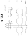
- FIG. 3 it illustrates waveforms which depict the operation of the timing system 10 when operative in the second mode wherein the bus timing clock is provided from an external source and the first generating means 14 generates the first and second microprocessor timing clocks in response to the second intermediate clock which is in turn derived by the buffer 12 from the externally generated bus timing clock.
- Illustrated in Figure 3 is the second intermediate timing clock 160, the first microprocessor timing clock (PH1) 162, the second microprocessor timing clock (PH2) 164, a microprocessor output 166 and an external bus input 168.
- the delay imposed upon the externally generated bus timing clock by the buffer 12 is negligible and therefore the second intermediate clock 160 substantially corresponds to or, in other words, is in phase with the externally generated bus timing clock.
- the output occurs after the aforementioned output delay which begins upon the common assertion of the first microprocessor timing clock 162 and the second intermediate clock 160.
- the total clock to output time is equal to the clock delay imposed by the first generating means 14 in generating the first microprocessor timing clock in response to the second intermediate clock plus the microprocessor output delay.
- the set-up time is illustrated at 170 and is the time from the occurrence of the input on the external bus to the next rising edge of the second intermediate clock. This is the set-up time seen by the external system.
- the real set-up time also includes an additional time period running from the rising edge of the second intermediate clock signal to the next rising edge of the first microprocessor timing clock and is represented at 172. This additional time period represents the time in which the microprocessor will next be able to initiate an output onto the external bus as, for example, when the microprocessor must change the condition of the external bus in response to the input 168.
Landscapes
- Engineering & Computer Science (AREA)
- Theoretical Computer Science (AREA)
- Physics & Mathematics (AREA)
- General Engineering & Computer Science (AREA)
- General Physics & Mathematics (AREA)
- Microcomputers (AREA)
- Information Transfer Systems (AREA)
- Synchronisation In Digital Transmission Systems (AREA)
- Hardware Redundancy (AREA)
Applications Claiming Priority (2)
| Application Number | Priority Date | Filing Date | Title |
|---|---|---|---|
| US647491 | 1991-01-28 | ||
| US07/647,491 US5291070A (en) | 1991-01-28 | 1991-01-28 | Microprocessor synchronous timing system |
Publications (3)
| Publication Number | Publication Date |
|---|---|
| EP0497441A2 true EP0497441A2 (de) | 1992-08-05 |
| EP0497441A3 EP0497441A3 (en) | 1993-04-21 |
| EP0497441B1 EP0497441B1 (de) | 1999-04-28 |
Family
ID=24597194
Family Applications (1)
| Application Number | Title | Priority Date | Filing Date |
|---|---|---|---|
| EP92300018A Expired - Lifetime EP0497441B1 (de) | 1991-01-28 | 1992-01-02 | Verbessertes synchronisches Taktsystem für Mikroprozessor |
Country Status (6)
| Country | Link |
|---|---|
| US (1) | US5291070A (de) |
| EP (1) | EP0497441B1 (de) |
| JP (1) | JP3272754B2 (de) |
| AT (1) | ATE179533T1 (de) |
| DE (1) | DE69229009T2 (de) |
| ES (1) | ES2130153T3 (de) |
Cited By (1)
| Publication number | Priority date | Publication date | Assignee | Title |
|---|---|---|---|---|
| EP0840237A1 (de) * | 1996-10-29 | 1998-05-06 | Matsushita Electric Industrial Co., Ltd. | Datenprozessorsynchronisation mit externem Bus |
Families Citing this family (12)
| Publication number | Priority date | Publication date | Assignee | Title |
|---|---|---|---|---|
| JPH05268016A (ja) * | 1992-02-19 | 1993-10-15 | Nec Corp | 半導体集積回路 |
| US5657457A (en) * | 1994-01-31 | 1997-08-12 | Dell Usa, L.P. | Method and apparatus for eliminating bus contention among multiple drivers without performance degradation |
| EP0721157A1 (de) * | 1994-12-12 | 1996-07-10 | Advanced Micro Devices, Inc. | Mikroprozessor mit auswählbarer Taktfrequenz |
| EP0821486B1 (de) * | 1996-07-24 | 2003-09-24 | STMicroelectronics S.r.l. | Taktschaltung mit Master-Slave-Synchronisierung |
| US7636803B2 (en) * | 2006-09-28 | 2009-12-22 | Advanced Micro Devices, Inc. | Device and method for transferring data between devices |
| US7737752B2 (en) * | 2007-05-17 | 2010-06-15 | Globalfoundries Inc | Techniques for integrated circuit clock management |
| US8014485B2 (en) * | 2007-05-17 | 2011-09-06 | Advanced Micro Devices, Inc. | Techniques for integrated circuit clock management using multiple clock generators |
| US7681099B2 (en) * | 2007-05-17 | 2010-03-16 | Advanced Micro Devices, Inc. | Techniques for integrated circuit clock signal manipulation to facilitate functional and speed test |
| US7921318B2 (en) * | 2007-05-17 | 2011-04-05 | Globalfoundries Inc. | Techniques for integrated circuit clock management using pulse skipping |
| US8575972B2 (en) * | 2009-03-23 | 2013-11-05 | Advanced Micro Devices, Inc. | Digital frequency synthesizer device and method thereof |
| KR102077684B1 (ko) * | 2013-01-09 | 2020-02-14 | 삼성전자주식회사 | 내부 스큐를 보상하는 반도체 장치 및 그것의 동작 방법 |
| EP4179232A1 (de) | 2020-07-10 | 2023-05-17 | Gualtiero Crozzoli | Differential mit kugeln oder rollen auf konvergenten elliptischen bahnen |
Family Cites Families (13)
| Publication number | Priority date | Publication date | Assignee | Title |
|---|---|---|---|---|
| GB1561961A (en) * | 1977-04-20 | 1980-03-05 | Int Computers Ltd | Data processing units |
| US4409671A (en) * | 1978-09-05 | 1983-10-11 | Motorola, Inc. | Data processor having single clock pin |
| US4596937A (en) * | 1982-04-28 | 1986-06-24 | International Computers Limited | Digital phase-locked loop |
| JPS6083166A (ja) * | 1983-10-14 | 1985-05-11 | Hitachi Ltd | 半導体集積回路装置 |
| JPS60204121A (ja) * | 1984-03-29 | 1985-10-15 | Fujitsu Ltd | 位相同期回路 |
| US4754164A (en) * | 1984-06-30 | 1988-06-28 | Unisys Corp. | Method for providing automatic clock de-skewing on a circuit board |
| US4691122A (en) * | 1985-03-29 | 1987-09-01 | Advanced Micro Devices, Inc. | CMOS D-type flip-flop circuits |
| US4675612A (en) * | 1985-06-21 | 1987-06-23 | Advanced Micro Devices, Inc. | Apparatus for synchronization of a first signal with a second signal |
| US4700084A (en) * | 1985-08-26 | 1987-10-13 | Rockwell International Corporation | Digital clock recovery circuit apparatus |
| US4929850A (en) * | 1987-09-17 | 1990-05-29 | Texas Instruments Incorporated | Metastable resistant flip-flop |
| JPH0198313A (ja) * | 1987-10-09 | 1989-04-17 | Nec Corp | 同期化回路 |
| US5059818A (en) * | 1990-06-01 | 1991-10-22 | Advanced Micro Devices, Inc. | Self-regulating clock generator |
| US5093581A (en) * | 1990-12-03 | 1992-03-03 | Thomson, S.A. | Circuitry for generating pulses of variable widths from binary input data |
-
1991
- 1991-01-28 US US07/647,491 patent/US5291070A/en not_active Expired - Lifetime
-
1992
- 1992-01-02 EP EP92300018A patent/EP0497441B1/de not_active Expired - Lifetime
- 1992-01-02 DE DE69229009T patent/DE69229009T2/de not_active Expired - Lifetime
- 1992-01-02 ES ES92300018T patent/ES2130153T3/es not_active Expired - Lifetime
- 1992-01-02 AT AT92300018T patent/ATE179533T1/de not_active IP Right Cessation
- 1992-01-24 JP JP01086892A patent/JP3272754B2/ja not_active Expired - Lifetime
Cited By (2)
| Publication number | Priority date | Publication date | Assignee | Title |
|---|---|---|---|---|
| EP0840237A1 (de) * | 1996-10-29 | 1998-05-06 | Matsushita Electric Industrial Co., Ltd. | Datenprozessorsynchronisation mit externem Bus |
| US5940599A (en) * | 1996-10-29 | 1999-08-17 | Matsushita Electric Industrial Co., Ltd. | Data processor |
Also Published As
| Publication number | Publication date |
|---|---|
| DE69229009T2 (de) | 1999-12-23 |
| US5291070A (en) | 1994-03-01 |
| JPH04304512A (ja) | 1992-10-27 |
| EP0497441B1 (de) | 1999-04-28 |
| ES2130153T3 (es) | 1999-07-01 |
| JP3272754B2 (ja) | 2002-04-08 |
| EP0497441A3 (en) | 1993-04-21 |
| ATE179533T1 (de) | 1999-05-15 |
| DE69229009D1 (de) | 1999-06-02 |
Similar Documents
| Publication | Publication Date | Title |
|---|---|---|
| KR100487206B1 (ko) | 다이나믹 웨이브-파이프라인 인터페이스 장치 및 그 방법 | |
| US6671753B2 (en) | Elastic interface apparatus and method therefor | |
| KR101014440B1 (ko) | 슬레이브 qdr2 호환 보조프로세서 | |
| US7111184B2 (en) | System and method for deterministic communication across clock domains | |
| EP0497441B1 (de) | Verbessertes synchronisches Taktsystem für Mikroprozessor | |
| US4745302A (en) | Asynchronous signal synchronizing circuit | |
| US6345328B1 (en) | Gear box for multiple clock domains | |
| US20100007383A1 (en) | Method and apparatus for generating a phase dependent control signal | |
| US5706484A (en) | Method for eliminating transition direction sensitive timing skews in a source synchronous design | |
| US5915107A (en) | Cross clock domain clocking for a system using two clock frequencies where one frequency is fractional multiple of the other | |
| KR100416208B1 (ko) | 코어 주파수의 기분수를 포함하는 주파수에서의 소스 동기전송을 위한 방법 및 장치 | |
| US5306962A (en) | Qualified non-overlapping clock generator to provide control lines with non-overlapping clock timing | |
| US5774001A (en) | Method for eliminating multiple output switching timing skews in a source synchronous design | |
| JP2914267B2 (ja) | 集積回路のデータ転送方法およびその装置 | |
| JP2004145709A (ja) | 半導体装置 | |
| US5706485A (en) | Method and apparatus for synchronizing clock signals in a multiple die circuit including a stop clock feature | |
| US4580243A (en) | Circuit for duplex synchronization of asynchronous signals | |
| US5896341A (en) | Synchronous semiconductor memory circuit | |
| US5701447A (en) | Method and apparatus for eliminating latch propagation delays in an alignment unit for use in a fractional bus architecture | |
| JP2684806B2 (ja) | 集積回路 | |
| US6236693B1 (en) | Generator for delay-matched clock and data signals | |
| JP3535243B2 (ja) | データ転送制御用クロック同期c素子群 | |
| JP3246443B2 (ja) | 同期式バッファ回路及びこれを用いたデータ伝送回路 | |
| JPS6235197B2 (de) | ||
| KR20010077601A (ko) | 지연 동기 루프를 사용하는 반도체 장치의 레이턴시 제어회로 |
Legal Events
| Date | Code | Title | Description |
|---|---|---|---|
| PUAI | Public reference made under article 153(3) epc to a published international application that has entered the european phase |
Free format text: ORIGINAL CODE: 0009012 |
|
| AK | Designated contracting states |
Kind code of ref document: A2 Designated state(s): AT BE CH DE DK ES FR GB GR IT LI LU NL PT SE |
|
| PUAL | Search report despatched |
Free format text: ORIGINAL CODE: 0009013 |
|
| AK | Designated contracting states |
Kind code of ref document: A3 Designated state(s): AT BE CH DE DK ES FR GB GR IT LI LU NL PT SE |
|
| 17P | Request for examination filed |
Effective date: 19931004 |
|
| 17Q | First examination report despatched |
Effective date: 19961008 |
|
| GRAG | Despatch of communication of intention to grant |
Free format text: ORIGINAL CODE: EPIDOS AGRA |
|
| GRAG | Despatch of communication of intention to grant |
Free format text: ORIGINAL CODE: EPIDOS AGRA |
|
| GRAH | Despatch of communication of intention to grant a patent |
Free format text: ORIGINAL CODE: EPIDOS IGRA |
|
| GRAH | Despatch of communication of intention to grant a patent |
Free format text: ORIGINAL CODE: EPIDOS IGRA |
|
| GRAA | (expected) grant |
Free format text: ORIGINAL CODE: 0009210 |
|
| AK | Designated contracting states |
Kind code of ref document: B1 Designated state(s): AT BE CH DE DK ES FR GB GR IT LI LU NL PT SE |
|
| PG25 | Lapsed in a contracting state [announced via postgrant information from national office to epo] |
Ref country code: IT Free format text: LAPSE BECAUSE OF FAILURE TO SUBMIT A TRANSLATION OF THE DESCRIPTION OR TO PAY THE FEE WITHIN THE PRESCRIBED TIME-LIMIT;WARNING: LAPSES OF ITALIAN PATENTS WITH EFFECTIVE DATE BEFORE 2007 MAY HAVE OCCURRED AT ANY TIME BEFORE 2007. THE CORRECT EFFECTIVE DATE MAY BE DIFFERENT FROM THE ONE RECORDED. Effective date: 19990428 Ref country code: LI Free format text: LAPSE BECAUSE OF FAILURE TO SUBMIT A TRANSLATION OF THE DESCRIPTION OR TO PAY THE FEE WITHIN THE PRESCRIBED TIME-LIMIT Effective date: 19990428 Ref country code: CH Free format text: LAPSE BECAUSE OF FAILURE TO SUBMIT A TRANSLATION OF THE DESCRIPTION OR TO PAY THE FEE WITHIN THE PRESCRIBED TIME-LIMIT Effective date: 19990428 Ref country code: AT Free format text: LAPSE BECAUSE OF FAILURE TO SUBMIT A TRANSLATION OF THE DESCRIPTION OR TO PAY THE FEE WITHIN THE PRESCRIBED TIME-LIMIT Effective date: 19990428 Ref country code: GR Free format text: LAPSE BECAUSE OF NON-PAYMENT OF DUE FEES Effective date: 19990428 Ref country code: SE Free format text: THE PATENT HAS BEEN ANNULLED BY A DECISION OF A NATIONAL AUTHORITY Effective date: 19990428 Ref country code: FR Free format text: LAPSE BECAUSE OF FAILURE TO SUBMIT A TRANSLATION OF THE DESCRIPTION OR TO PAY THE FEE WITHIN THE PRESCRIBED TIME-LIMIT Effective date: 19990428 Ref country code: BE Free format text: LAPSE BECAUSE OF FAILURE TO SUBMIT A TRANSLATION OF THE DESCRIPTION OR TO PAY THE FEE WITHIN THE PRESCRIBED TIME-LIMIT Effective date: 19990428 |
|
| REF | Corresponds to: |
Ref document number: 179533 Country of ref document: AT Date of ref document: 19990515 Kind code of ref document: T |
|
| REG | Reference to a national code |
Ref country code: CH Ref legal event code: EP |
|
| REF | Corresponds to: |
Ref document number: 69229009 Country of ref document: DE Date of ref document: 19990602 |
|
| REG | Reference to a national code |
Ref country code: ES Ref legal event code: FG2A Ref document number: 2130153 Country of ref document: ES Kind code of ref document: T3 |
|
| PG25 | Lapsed in a contracting state [announced via postgrant information from national office to epo] |
Ref country code: DK Free format text: LAPSE BECAUSE OF FAILURE TO SUBMIT A TRANSLATION OF THE DESCRIPTION OR TO PAY THE FEE WITHIN THE PRESCRIBED TIME-LIMIT Effective date: 19990728 |
|
| PG25 | Lapsed in a contracting state [announced via postgrant information from national office to epo] |
Ref country code: PT Free format text: LAPSE BECAUSE OF FAILURE TO SUBMIT A TRANSLATION OF THE DESCRIPTION OR TO PAY THE FEE WITHIN THE PRESCRIBED TIME-LIMIT Effective date: 19990729 |
|
| EN | Fr: translation not filed | ||
| REG | Reference to a national code |
Ref country code: CH Ref legal event code: PL |
|
| PG25 | Lapsed in a contracting state [announced via postgrant information from national office to epo] |
Ref country code: LU Free format text: LAPSE BECAUSE OF NON-PAYMENT OF DUE FEES Effective date: 20000102 |
|
| PG25 | Lapsed in a contracting state [announced via postgrant information from national office to epo] |
Ref country code: ES Free format text: THE PATENT HAS BEEN ANNULLED BY A DECISION OF A NATIONAL AUTHORITY Effective date: 20000103 |
|
| PLBE | No opposition filed within time limit |
Free format text: ORIGINAL CODE: 0009261 |
|
| 26N | No opposition filed | ||
| REG | Reference to a national code |
Ref country code: GB Ref legal event code: IF02 |
|
| REG | Reference to a national code |
Ref country code: ES Ref legal event code: FD2A Effective date: 20020304 |
|
| PGFP | Annual fee paid to national office [announced via postgrant information from national office to epo] |
Ref country code: GB Payment date: 20101215 Year of fee payment: 20 |
|
| PGFP | Annual fee paid to national office [announced via postgrant information from national office to epo] |
Ref country code: DE Payment date: 20110131 Year of fee payment: 20 Ref country code: NL Payment date: 20110117 Year of fee payment: 20 |
|
| REG | Reference to a national code |
Ref country code: DE Ref legal event code: R071 Ref document number: 69229009 Country of ref document: DE |
|
| REG | Reference to a national code |
Ref country code: DE Ref legal event code: R071 Ref document number: 69229009 Country of ref document: DE |
|
| REG | Reference to a national code |
Ref country code: NL Ref legal event code: V4 Effective date: 20120102 |
|
| REG | Reference to a national code |
Ref country code: GB Ref legal event code: PE20 Expiry date: 20120101 |
|
| PG25 | Lapsed in a contracting state [announced via postgrant information from national office to epo] |
Ref country code: GB Free format text: LAPSE BECAUSE OF EXPIRATION OF PROTECTION Effective date: 20120101 |
|
| PG25 | Lapsed in a contracting state [announced via postgrant information from national office to epo] |
Ref country code: DE Free format text: LAPSE BECAUSE OF EXPIRATION OF PROTECTION Effective date: 20120103 |