EP0503731A1 - Verfahren zur Realisierung eines Transistors mit hoher Elektronenbeweglichkeit - Google Patents
Verfahren zur Realisierung eines Transistors mit hoher Elektronenbeweglichkeit Download PDFInfo
- Publication number
- EP0503731A1 EP0503731A1 EP92200654A EP92200654A EP0503731A1 EP 0503731 A1 EP0503731 A1 EP 0503731A1 EP 92200654 A EP92200654 A EP 92200654A EP 92200654 A EP92200654 A EP 92200654A EP 0503731 A1 EP0503731 A1 EP 0503731A1
- Authority
- EP
- European Patent Office
- Prior art keywords
- layer
- transistor
- mesa
- layers
- etching
- Prior art date
- Legal status (The legal status is an assumption and is not a legal conclusion. Google has not performed a legal analysis and makes no representation as to the accuracy of the status listed.)
- Granted
Links
Images

Classifications
-
- H—ELECTRICITY
- H10—SEMICONDUCTOR DEVICES; ELECTRIC SOLID-STATE DEVICES NOT OTHERWISE PROVIDED FOR
- H10D—INORGANIC ELECTRIC SEMICONDUCTOR DEVICES
- H10D30/00—Field-effect transistors [FET]
- H10D30/01—Manufacture or treatment
- H10D30/015—Manufacture or treatment of FETs having heterojunction interface channels or heterojunction gate electrodes, e.g. HEMT
-
- H—ELECTRICITY
- H10—SEMICONDUCTOR DEVICES; ELECTRIC SOLID-STATE DEVICES NOT OTHERWISE PROVIDED FOR
- H10W—GENERIC PACKAGES, INTERCONNECTIONS, CONNECTORS OR OTHER CONSTRUCTIONAL DETAILS OF DEVICES COVERED BY CLASS H10
- H10W10/00—Isolation regions in semiconductor bodies between components of integrated devices
-
- H—ELECTRICITY
- H10—SEMICONDUCTOR DEVICES; ELECTRIC SOLID-STATE DEVICES NOT OTHERWISE PROVIDED FOR
- H10W—GENERIC PACKAGES, INTERCONNECTIONS, CONNECTORS OR OTHER CONSTRUCTIONAL DETAILS OF DEVICES COVERED BY CLASS H10
- H10W10/00—Isolation regions in semiconductor bodies between components of integrated devices
- H10W10/01—Manufacture or treatment
-
- Y—GENERAL TAGGING OF NEW TECHNOLOGICAL DEVELOPMENTS; GENERAL TAGGING OF CROSS-SECTIONAL TECHNOLOGIES SPANNING OVER SEVERAL SECTIONS OF THE IPC; TECHNICAL SUBJECTS COVERED BY FORMER USPC CROSS-REFERENCE ART COLLECTIONS [XRACs] AND DIGESTS
- Y10—TECHNICAL SUBJECTS COVERED BY FORMER USPC
- Y10S—TECHNICAL SUBJECTS COVERED BY FORMER USPC CROSS-REFERENCE ART COLLECTIONS [XRACs] AND DIGESTS
- Y10S977/00—Nanotechnology
- Y10S977/70—Nanostructure
- Y10S977/701—Integrated with dissimilar structures on a common substrate
- Y10S977/712—Integrated with dissimilar structures on a common substrate formed from plural layers of nanosized material, e.g. stacked structures
-
- Y—GENERAL TAGGING OF NEW TECHNOLOGICAL DEVELOPMENTS; GENERAL TAGGING OF CROSS-SECTIONAL TECHNOLOGIES SPANNING OVER SEVERAL SECTIONS OF THE IPC; TECHNICAL SUBJECTS COVERED BY FORMER USPC CROSS-REFERENCE ART COLLECTIONS [XRACs] AND DIGESTS
- Y10—TECHNICAL SUBJECTS COVERED BY FORMER USPC
- Y10S—TECHNICAL SUBJECTS COVERED BY FORMER USPC CROSS-REFERENCE ART COLLECTIONS [XRACs] AND DIGESTS
- Y10S977/00—Nanotechnology
- Y10S977/70—Nanostructure
- Y10S977/701—Integrated with dissimilar structures on a common substrate
- Y10S977/723—On an electrically insulating substrate
-
- Y—GENERAL TAGGING OF NEW TECHNOLOGICAL DEVELOPMENTS; GENERAL TAGGING OF CROSS-SECTIONAL TECHNOLOGIES SPANNING OVER SEVERAL SECTIONS OF THE IPC; TECHNICAL SUBJECTS COVERED BY FORMER USPC CROSS-REFERENCE ART COLLECTIONS [XRACs] AND DIGESTS
- Y10—TECHNICAL SUBJECTS COVERED BY FORMER USPC
- Y10S—TECHNICAL SUBJECTS COVERED BY FORMER USPC CROSS-REFERENCE ART COLLECTIONS [XRACs] AND DIGESTS
- Y10S977/00—Nanotechnology
- Y10S977/70—Nanostructure
- Y10S977/755—Nanosheet or quantum barrier/well, i.e. layer structure having one dimension or thickness of 100 nm or less
Definitions
- the invention relates to a method for producing an integrated circuit on a substrate comprising steps for forming a high electron mobility transistor (HEMT), these steps including the realization of a stack of layers, produced on the substrate, among which there is at least one layer of a material with a small prohibited bandwidth, lightly doped, to form the channel of the transistor, and a donor layer with a material with a large prohibited bandwidth, heavily doped, to supply electrons, and these stages including the creation of an isolation zone with respect to the other elements of the integrated circuit all around the transistor and the production of gate, source and drain electrodes .
- HEMT high electron mobility transistor
- the invention finds its application in the production of digital or analog integrated circuits.
- the cited document describes a method for producing an integrated circuit including the formation of a transistor with high electronic mobility.
- This method comprises producing, on a semi-insulating InP substrate, a succession of layers respectively a buffer layer of AlInAs n ⁇ , a channel layer of GaInAs nn ⁇ , a spacer layer of AlInAs n ⁇ , a donor layer of AlInAs n+ (heavily doped), a layer suitable for receiving a Schottky contact made of AlInAS n ⁇ and a GaInAs encapsulation layer.
- two ohmic type contacts are made to constitute the source and the drain of the transistor, on the surface of the encapsulation layer. Then a groove is etched between the source and the drain to the so-called Schottky layer, and a Schottky type contact is made by metallization in this groove, to form the gate of the transistor, by self-alignment.
- the first method taught is isolation by forming an MESA, that is to say by carrying out etching all around the region of the transistor, this etching delimiting the transistor whose active region is then in relief in relation to the substrate. Under these conditions, it is necessary for the metallization of the Schottky grid to follow the flank of the MESA in order to connect the grid to a grid pad disposed near the transistor in the region of the substrate which appears after etching of the MESA, as shown on Figure 3 of the cited document.
- connection metallization is in contact with all the layers which are flush with the side of the MESA and in particular the heavily doped layer of AlInAs n+, and, in operation, the transistor is affected by a high leakage current, as shown in Figure 2 of the cited document.
- this leakage current is avoided by carrying out the isolation of the transistor, not by the formation of a MESA, but by a second method consisting in implanting ions around the active area, resulting in the fact that the device remains planar.
- the second solution taught does not have the favor of a person skilled in the art of circuit manufacturer. integrated. Indeed, ion implantation to achieve insulation implements expensive technical means consisting of an ion implantation device; moreover, it requires annealing which tends to deteriorate the properties of the layers, or of other integrated circuit devices, already produced; then the ion implantation is not correctly repetitive; moreover, its effectiveness is less than that of a MESA. From all these facts, it follows first of all that the manufacturing yield of an integrated circuit including isolation steps by ion implantation may be found to be considerably restricted instead of reaching figures as close as possible to 100% as hoped by the manufacturer of integrated circuits, and it follows that the cost of the integrated circuit is high.
- the invention relates to an advantageous production method of a high electronic mobility transistor (in English HEMT) in manufacturing synergy with the other elements of an integrated circuit.
- HEMT high electronic mobility transistor
- This transistor comprises a stack of layers produced on a substrate, among which there is preferably a first layer 31 of a material with a small band gap, lightly doped to form the channel of the transitor, a second layer 22 of a material of width larger forbidden band lightly doped so that a two-dimensional electron gas can form at the interface with said first layer 31, and to spatially separate the electrons of this two-dimensional gas from the charges of the next layer, and a third layer 23 material with a large forbidden bandwidth, heavily doped to supply electrons which can be transferred into the two-dimensional gas.
- the transistor is further provided with means of isolation with respect to other integrated circuit elements produced on the same substrate.
- these isolation means consist in producing an MESA, and not an ion implantation considered to be costly and unfavorable in the integrated circuit industry.
- An object of the invention is to provide a method for producing such a HEMT which is devoid of the leakage currents which would appear in the transistor during its operation, if due to the MESA, the gate metallization G were to come into contact with the heavily doped layer included in the active region and which is flush with the flanks of the MESA.
- Another object of the invention is to provide such a method suitable for being implemented without replacing the costly known ion implantation step with other steps just as costly to achieve the aforementioned object, such as for example one or more additional masking steps (a masking step being considered expensive because it includes substeps for defining an optical mask which is always expensive and then implementing photolithography).
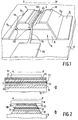
- Figure 1 shows in perspective a simplified representation of a HEMT transistor obtained by the method according to the invention.
- This transistor comprises, erected on a substrate 10, a stack 11 of several semiconductor layers. It further comprises, on the surface of these layers called active layers, respectively a source electrode S, a gate electrode G and a drain electrode D.
- the erected structure is called MESA.
- the source, gate and drain electrodes are connected by metal connections, respectively C S , C G and C D , to source, gate and drain pads, respectively P S , P G and P D arranged around the MESA on the substrate 10 in non-active regions.
- the substrate 10 is favorable for the substrate 10 to be semi-insulating.
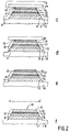
- the metal connections C S , C G and C D are therefore arranged along the sides 100 of the MESA. To avoid contact of these connections, and in particular contact of the gate connection C G , with the heavily doped layer, for example 23, along the flanks 100 of the MESA, these flanks 100 are provided with a dielectric layer K , performing electrical insulation, during the MESA production stages, without extending the production process of the integrated circuit in which the HEMT is included, or increasing its cost.
- Tests carried out on the HEMT transistor obtained by the method according to the invention show that the leakage current of the transistor working under the same conditions as that of the state of the art cited, is just as low, this rather by reference with the text of the cited document than with the figure presented, the scale of which does not make it possible to really appreciate the value of the leakage current in reverse of the transistor mounted as a diode. In the transistor obtained by the method of the invention, this leakage current can be considered as zero. On the other hand, live, the performance of the transistor according to the invention is improved, compared to that of the known transistor.
- the indication of the concentration of indium in the material provides the preferred concentration of indium in the ternary material to obtain the mesh agreement with the substrate in InP.
- the metal to make the Schottky contact of grid G will favorably be the TiPtAu alloy.
- the metallization of the ohmic contacts of source S and drain D will be favorably obtained by means of deposition of AuGe / Ni / Au.
- the buffer layer 21 may optionally, in a variant, be replaced by a superlattice.
Landscapes
- Junction Field-Effect Transistors (AREA)
- Structures Or Materials For Encapsulating Or Coating Semiconductor Devices Or Solid State Devices (AREA)
Applications Claiming Priority (2)
| Application Number | Priority Date | Filing Date | Title |
|---|---|---|---|
| FR9103198 | 1991-03-15 | ||
| FR9103198 | 1991-03-15 |
Publications (2)
| Publication Number | Publication Date |
|---|---|
| EP0503731A1 true EP0503731A1 (de) | 1992-09-16 |
| EP0503731B1 EP0503731B1 (de) | 1998-12-02 |
Family
ID=9410807
Family Applications (1)
| Application Number | Title | Priority Date | Filing Date |
|---|---|---|---|
| EP92200654A Expired - Lifetime EP0503731B1 (de) | 1991-03-15 | 1992-03-06 | Verfahren zur Realisierung eines Transistors mit hoher Elektronenbeweglichkeit |
Country Status (4)
| Country | Link |
|---|---|
| US (1) | US5358878A (de) |
| EP (1) | EP0503731B1 (de) |
| JP (1) | JPH0766959B2 (de) |
| DE (1) | DE69227712T2 (de) |
Families Citing this family (11)
| Publication number | Priority date | Publication date | Assignee | Title |
|---|---|---|---|---|
| JP2606581B2 (ja) * | 1994-05-18 | 1997-05-07 | 日本電気株式会社 | 電界効果トランジスタ及びその製造方法 |
| JP3368452B2 (ja) * | 1995-04-25 | 2003-01-20 | 富士通株式会社 | 化合物半導体装置及びその製造方法 |
| US5856217A (en) * | 1997-04-10 | 1999-01-05 | Hughes Electronics Corporation | Modulation-doped field-effect transistors and fabrication processes |
| US6287946B1 (en) * | 1999-05-05 | 2001-09-11 | Hrl Laboratories, Llc | Fabrication of low resistance, non-alloyed, ohmic contacts to InP using non-stoichiometric InP layers |
| CA2456662A1 (en) * | 2001-08-07 | 2003-02-20 | Jan Kuzmik | High electron mobility devices |
| JP4822667B2 (ja) * | 2004-01-23 | 2011-11-24 | Okiセミコンダクタ株式会社 | 半導体素子及びその製造方法 |
| US7750370B2 (en) * | 2007-12-20 | 2010-07-06 | Northrop Grumman Space & Mission Systems Corp. | High electron mobility transistor having self-aligned miniature field mitigating plate on a protective dielectric layer |
| US10134839B2 (en) * | 2015-05-08 | 2018-11-20 | Raytheon Company | Field effect transistor structure having notched mesa |
| CN106686932B (zh) | 2015-11-05 | 2019-12-13 | 精能医学股份有限公司 | 植入式电子装置的防水结构 |
| CN112614886B (zh) * | 2020-12-16 | 2022-11-22 | 广东省科学院半导体研究所 | 一种hemt器件及其制作方法 |
| CN116960150A (zh) * | 2022-04-19 | 2023-10-27 | 联华电子股份有限公司 | 高电子迁移率晶体管 |
Citations (1)
| Publication number | Priority date | Publication date | Assignee | Title |
|---|---|---|---|---|
| US4545109A (en) * | 1983-01-21 | 1985-10-08 | Rca Corporation | Method of making a gallium arsenide field effect transistor |
Family Cites Families (1)
| Publication number | Priority date | Publication date | Assignee | Title |
|---|---|---|---|---|
| DE3279795D1 (en) * | 1981-04-23 | 1989-08-03 | Fujitsu Ltd | High electron mobility semiconductor device |
-
1992
- 1992-03-06 DE DE69227712T patent/DE69227712T2/de not_active Expired - Fee Related
- 1992-03-06 EP EP92200654A patent/EP0503731B1/de not_active Expired - Lifetime
- 1992-03-09 US US07/848,615 patent/US5358878A/en not_active Expired - Lifetime
- 1992-03-16 JP JP4058185A patent/JPH0766959B2/ja not_active Expired - Fee Related
Patent Citations (1)
| Publication number | Priority date | Publication date | Assignee | Title |
|---|---|---|---|---|
| US4545109A (en) * | 1983-01-21 | 1985-10-08 | Rca Corporation | Method of making a gallium arsenide field effect transistor |
Non-Patent Citations (3)
| Title |
|---|
| GAAS IC SYMPOSIUM TECHNICAL DIGEST 22 Octobre 1989, SAN DIEGO USA pages 143 - 146; A. S. BROWN ET.AL.: 'LOW-TEMPERATURE BUFFER AlInAs/GaInAs ON InP HEMT TECHNOLOGY FOR ULTRA-HIGH-SPEED INTEGRATED CIRCUITS' * |
| PATENT ABSTRACTS OF JAPAN vol. 11, no. 41 (E-478)(2488) 6 Février 1987 & JP-A-61 207 080 ( SHARP ) 13 Septembre 1986 * |
| PATENT ABSTRACTS OF JAPAN vol. 14, no. 463 (E-988)(4406) 8 Octobre 1990 & JP-A-2 188 930 ( SUMITOMO ELECTRIC ) 25 Juillet 1990 * |
Also Published As
| Publication number | Publication date |
|---|---|
| JPH0575046A (ja) | 1993-03-26 |
| JPH0766959B2 (ja) | 1995-07-19 |
| US5358878A (en) | 1994-10-25 |
| EP0503731B1 (de) | 1998-12-02 |
| DE69227712T2 (de) | 1999-06-24 |
| DE69227712D1 (de) | 1999-01-14 |
Similar Documents
| Publication | Publication Date | Title |
|---|---|---|
| JP6382396B2 (ja) | 量子井戸トランジスタへのコンタクトを形成する方法 | |
| EP0005720A1 (de) | Verfahren zur Herstellung eines Feldeffekttransistors mit isoliertem Gate und sehr kurzem effektiven Kanal | |
| EP0503731B1 (de) | Verfahren zur Realisierung eines Transistors mit hoher Elektronenbeweglichkeit | |
| EP3240041A1 (de) | Selbstsperrender transistor mit heteroübergang und hoher schwellenspannung | |
| EP3913687B1 (de) | Elektronisches bauelement mit heteroübergang mit einer feldplatte und einem p-dotierten schwebenden bereich | |
| EP3549172A1 (de) | Heteroübergangstransistor mit vertikaler struktur | |
| EP3378098B1 (de) | Heteroübergangdiode mit erhöhtem transientem spitzenstrom | |
| EP0149390B1 (de) | Feldeffekttransistor mit vertikaler Sub-Mikronstruktur und Verfahren zu dessen Herstellung | |
| FR2493604A1 (fr) | Transistors a effet de champ a grille ultra courte | |
| EP3826061B1 (de) | Hybride elektronische vorrichtung und verfahren zur herstellung einer solchen vorrichtung | |
| FR2655774A1 (fr) | Perfectionnement aux transistors de puissance en materiaux iii-v sur substrat silicium et procede de fabrication. | |
| FR2489045A1 (fr) | Transistor a effet de champ gaas a memoire non volatile | |
| EP3561880A1 (de) | Hemt und herstellungsverfahren welches eine geringere gatelänge und einen geringeren gate-leckverlust begünstigt | |
| FR2496990A1 (fr) | Transistor a effet de champ a barriere schottky | |
| FR2758207A1 (fr) | Procede de fabrication d'un dispositif a semiconducteur composite haute vitesse presentant une capacite et une resistance parasites minimisees et un hemt, un mesfet et un hbt selon ce procede | |
| EP3826072A1 (de) | Elektronengas-transistor, monoblock-vorrichtung, die mindestens zwei transistoren in kaskadenschaltung umfasst, und entsprechendes herstellungsverfahren | |
| WO2019224448A1 (fr) | Transistor a haute mobilite electronique en mode enrichissement | |
| EP1517377A1 (de) | Bipolartransistor | |
| FR2864345A1 (fr) | Realisation de la peripherie d'une diode schottky a tranchees mos | |
| FR3035265A1 (fr) | Procede de fabrication de transistors soi pour une densite d'integration accrue | |
| WO2018007711A1 (fr) | Dispositif cascode integre monolithiquement | |
| EP0570257A1 (de) | Feldeffekt-Halbleiteranordnung mit sekundärem Gate, Verfahren zur Herstellung und Verwendung in einer Matrix-Ansteuerungsanordnung | |
| EP3792982A1 (de) | Elektronische leistungsvorrichtung mit superjunction | |
| FR3053832A1 (fr) | Procede de fabrication d'un transistor a heterojonction a effet de champ et transistor correspondant | |
| FR3142604A1 (fr) | Dispositif microélectronique à tenue en tension verticale améliorée |
Legal Events
| Date | Code | Title | Description |
|---|---|---|---|
| PUAI | Public reference made under article 153(3) epc to a published international application that has entered the european phase |
Free format text: ORIGINAL CODE: 0009012 |
|
| AK | Designated contracting states |
Kind code of ref document: A1 Designated state(s): DE FR GB |
|
| 17P | Request for examination filed |
Effective date: 19930305 |
|
| RAP1 | Party data changed (applicant data changed or rights of an application transferred) |
Owner name: LABORATOIRES D'ELECTRONIQUE PHILIPS S.A.S. Owner name: PHILIPS ELECTRONICS N.V. |
|
| GRAG | Despatch of communication of intention to grant |
Free format text: ORIGINAL CODE: EPIDOS AGRA |
|
| 17Q | First examination report despatched |
Effective date: 19980206 |
|
| GRAG | Despatch of communication of intention to grant |
Free format text: ORIGINAL CODE: EPIDOS AGRA |
|
| GRAH | Despatch of communication of intention to grant a patent |
Free format text: ORIGINAL CODE: EPIDOS IGRA |
|
| RAP3 | Party data changed (applicant data changed or rights of an application transferred) |
Owner name: LABORATOIRES D'ELECTRONIQUE PHILIPS S.A.S. Owner name: KONINKLIJKE PHILIPS ELECTRONICS N.V. |
|
| GRAH | Despatch of communication of intention to grant a patent |
Free format text: ORIGINAL CODE: EPIDOS IGRA |
|
| GRAA | (expected) grant |
Free format text: ORIGINAL CODE: 0009210 |
|
| AK | Designated contracting states |
Kind code of ref document: B1 Designated state(s): DE FR GB |
|
| REF | Corresponds to: |
Ref document number: 69227712 Country of ref document: DE Date of ref document: 19990114 |
|
| GBT | Gb: translation of ep patent filed (gb section 77(6)(a)/1977) |
Effective date: 19990106 |
|
| PLBE | No opposition filed within time limit |
Free format text: ORIGINAL CODE: 0009261 |
|
| STAA | Information on the status of an ep patent application or granted ep patent |
Free format text: STATUS: NO OPPOSITION FILED WITHIN TIME LIMIT |
|
| 26N | No opposition filed | ||
| REG | Reference to a national code |
Ref country code: FR Ref legal event code: TP |
|
| REG | Reference to a national code |
Ref country code: GB Ref legal event code: IF02 |
|
| REG | Reference to a national code |
Ref country code: GB Ref legal event code: 746 Effective date: 20021017 |
|
| REG | Reference to a national code |
Ref country code: FR Ref legal event code: D6 |
|
| PGFP | Annual fee paid to national office [announced via postgrant information from national office to epo] |
Ref country code: GB Payment date: 20070327 Year of fee payment: 16 |
|
| PGFP | Annual fee paid to national office [announced via postgrant information from national office to epo] |
Ref country code: DE Payment date: 20070516 Year of fee payment: 16 |
|
| PGFP | Annual fee paid to national office [announced via postgrant information from national office to epo] |
Ref country code: FR Payment date: 20070329 Year of fee payment: 16 |
|
| GBPC | Gb: european patent ceased through non-payment of renewal fee |
Effective date: 20080306 |
|
| REG | Reference to a national code |
Ref country code: FR Ref legal event code: ST Effective date: 20081125 |
|
| PG25 | Lapsed in a contracting state [announced via postgrant information from national office to epo] |
Ref country code: DE Free format text: LAPSE BECAUSE OF NON-PAYMENT OF DUE FEES Effective date: 20081001 |
|
| PG25 | Lapsed in a contracting state [announced via postgrant information from national office to epo] |
Ref country code: FR Free format text: LAPSE BECAUSE OF NON-PAYMENT OF DUE FEES Effective date: 20080331 |
|
| PG25 | Lapsed in a contracting state [announced via postgrant information from national office to epo] |
Ref country code: GB Free format text: LAPSE BECAUSE OF NON-PAYMENT OF DUE FEES Effective date: 20080306 |