EP0503904B1 - Gestapelte CMOS Halbleitervorrichtung und Verfahren zu ihrer Herstellung - Google Patents
Gestapelte CMOS Halbleitervorrichtung und Verfahren zu ihrer Herstellung Download PDFInfo
- Publication number
- EP0503904B1 EP0503904B1 EP92302045A EP92302045A EP0503904B1 EP 0503904 B1 EP0503904 B1 EP 0503904B1 EP 92302045 A EP92302045 A EP 92302045A EP 92302045 A EP92302045 A EP 92302045A EP 0503904 B1 EP0503904 B1 EP 0503904B1
- Authority
- EP
- European Patent Office
- Prior art keywords
- layer
- conductivity type
- ions
- insulation layer
- dopant impurity
- Prior art date
- Legal status (The legal status is an assumption and is not a legal conclusion. Google has not performed a legal analysis and makes no representation as to the accuracy of the status listed.)
- Expired - Lifetime
Links
Images


Classifications
-
- H—ELECTRICITY
- H10—SEMICONDUCTOR DEVICES; ELECTRIC SOLID-STATE DEVICES NOT OTHERWISE PROVIDED FOR
- H10B—ELECTRONIC MEMORY DEVICES
- H10B10/00—Static random access memory [SRAM] devices
- H10B10/12—Static random access memory [SRAM] devices comprising a MOSFET load element
-
- H—ELECTRICITY
- H10—SEMICONDUCTOR DEVICES; ELECTRIC SOLID-STATE DEVICES NOT OTHERWISE PROVIDED FOR
- H10W—GENERIC PACKAGES, INTERCONNECTIONS, CONNECTORS OR OTHER CONSTRUCTIONAL DETAILS OF DEVICES COVERED BY CLASS H10
- H10W20/00—Interconnections in chips, wafers or substrates
- H10W20/01—Manufacture or treatment
- H10W20/031—Manufacture or treatment of conductive parts of the interconnections
- H10W20/069—Manufacture or treatment of conductive parts of the interconnections by forming self-aligned vias or self-aligned contact plugs
-
- H—ELECTRICITY
- H10—SEMICONDUCTOR DEVICES; ELECTRIC SOLID-STATE DEVICES NOT OTHERWISE PROVIDED FOR
- H10W—GENERIC PACKAGES, INTERCONNECTIONS, CONNECTORS OR OTHER CONSTRUCTIONAL DETAILS OF DEVICES COVERED BY CLASS H10
- H10W20/00—Interconnections in chips, wafers or substrates
- H10W20/40—Interconnections external to wafers or substrates, e.g. back-end-of-line [BEOL] metallisations or vias connecting to gate electrodes
- H10W20/41—Interconnections external to wafers or substrates, e.g. back-end-of-line [BEOL] metallisations or vias connecting to gate electrodes characterised by their conductive parts
- H10W20/44—Conductive materials thereof
- H10W20/4451—Semiconductor materials, e.g. polysilicon
-
- H—ELECTRICITY
- H10—SEMICONDUCTOR DEVICES; ELECTRIC SOLID-STATE DEVICES NOT OTHERWISE PROVIDED FOR
- H10W—GENERIC PACKAGES, INTERCONNECTIONS, CONNECTORS OR OTHER CONSTRUCTIONAL DETAILS OF DEVICES COVERED BY CLASS H10
- H10W20/00—Interconnections in chips, wafers or substrates
- H10W20/01—Manufacture or treatment
- H10W20/031—Manufacture or treatment of conductive parts of the interconnections
- H10W20/064—Manufacture or treatment of conductive parts of the interconnections by modifying the conductivity of conductive parts, e.g. by alloying
-
- H—ELECTRICITY
- H10—SEMICONDUCTOR DEVICES; ELECTRIC SOLID-STATE DEVICES NOT OTHERWISE PROVIDED FOR
- H10W—GENERIC PACKAGES, INTERCONNECTIONS, CONNECTORS OR OTHER CONSTRUCTIONAL DETAILS OF DEVICES COVERED BY CLASS H10
- H10W20/00—Interconnections in chips, wafers or substrates
- H10W20/01—Manufacture or treatment
- H10W20/031—Manufacture or treatment of conductive parts of the interconnections
- H10W20/064—Manufacture or treatment of conductive parts of the interconnections by modifying the conductivity of conductive parts, e.g. by alloying
- H10W20/066—Manufacture or treatment of conductive parts of the interconnections by modifying the conductivity of conductive parts, e.g. by alloying by forming silicides of refractory metals
-
- Y—GENERAL TAGGING OF NEW TECHNOLOGICAL DEVELOPMENTS; GENERAL TAGGING OF CROSS-SECTIONAL TECHNOLOGIES SPANNING OVER SEVERAL SECTIONS OF THE IPC; TECHNICAL SUBJECTS COVERED BY FORMER USPC CROSS-REFERENCE ART COLLECTIONS [XRACs] AND DIGESTS
- Y10—TECHNICAL SUBJECTS COVERED BY FORMER USPC
- Y10S—TECHNICAL SUBJECTS COVERED BY FORMER USPC CROSS-REFERENCE ART COLLECTIONS [XRACs] AND DIGESTS
- Y10S257/00—Active solid-state devices, e.g. transistors, solid-state diodes
- Y10S257/903—FET configuration adapted for use as static memory cell
Definitions
- the present invention concerns stacked type semiconductor devices, in particular devices - e.g. Static Random Access Memories - in which interconnection is provided between complementary MOS transistors at different levels. It is also concerned with their manufacture.
- FIG. 1 through 3 show a structure of a memory cell of a CMOS type SRAM using a thin film transistor as a load, which is shown in "A Memory Cell with Polysilicon Thin Film Transistor (TFT) for a 4Mbit SRAM", Tsutsumi et al., Institute of Electronics and Communication Engineers of Japan Technical Report, Vol. 90, No. 48, p7 - p13.
- Fig. 4 is an equivalent circuit diagram of the memory cell of the SRAM. Referring to Fig.
- a memory cell of a CMOS type SRAM has a pair of CMOS inverters.
- One CMOS inverter has an n channel MOS drive transistor 20a and a p channel MOS thin film load transistor 21a.
- the other CMOS inverter has an n channel MOS drive transistor 20b and a p channel MOS thin film load transistor 21b.
- the gates of transistors 20a, 21a of said one CMOS inverter are cross connected to a store node 25b common to transistors 20b, 21b of said the other CMOS inverter, and the gates of transistors 20b, 21b of said the other CMOS inverter are cross-connected to a stored node 25a common to transistors 20a, 21a of said one CMOS inverter to constitute a flip-flop circuit.
- the sources of p channel MOS thin film load transistors 21a, 21b are connected to a power supply 23.
- Each of the sources of n channel MOS drive transistors 20a, 20b is connected to ground.
- Store nodes 25a, 25b of the flip-flop circuit are connected respectively to n channel MOS transfer transistors 22a, 22b.
- the gates of n channel MOS transfer transistors 22a, 22b are connected to a word line 27.
- the drain regions of n channel MOS transfer transistors 22a, 22b are respectively connected to bit lines 26a, 26
- bit line 26a is set at a ground level, and bit line 26b at a power supply level.
- N channel MOS transfer transistors 22a, 22b are turned on by applying a prescribed potential to word line 27.
- Bit lines 26a, 26b are connected to a sense amplifier circuit. Under the condition, word line 27 is supplied with a prescribed potential to turn on n channel MOS transfer transistors 22a, 22b. As a result, potentials of store nodes 25a, 25b are read to bit lines 26a, 26b.
- Figs. 2 and 3 are plan structural views of the memory cell.
- the memory cell is divided into a lower layer portion and an upper layer portion of a substrate to show a plan structure of the lower layer portion of the memory cell in Fig. 2 and a plan structure of the upper layer portion in Fig. 3 .
- Fig. 1 is a sectional structural view taken along line X-X in Figs. 2 and 3..
- the memory cell of an SRAM comprises n channel MOS drive transistors 20a, 20b and n channel MOS transfer transistors 22a, 22b, etc. in a lower region closer to a surface of a silicon substrate 1.
- P channel MOS thin film load transistors 21a, 21b are arranged in an upper region formed on a main surface of silicon substrate 1 with an interlevel insulating layer 9 interposed.
- a p well region 2 is formed on a surface of silicon substrate 1.
- a field oxide film 4 and a p + isolation region 3 are formed in an isolation region on a main surface of p well region 2.
- An n channel MOS drive transistor 20a and an n channel MOS transfer transistor 22b each comprises n + source/drain regions 7, 7, a gate oxide film 5 and gate electrode 6.
- Gate electrode 6 has a polycide structure formed of a polycrystalline silicon layer 6a and a metal silicide film 6b which was formed on a polycrystalline silicon layer 6a.
- a thin film transistor 14 comprises a gate electrode 8b formed on the surface of interlevel insulating layer 9, a gate oxide film 13 covering a surface of gate electrode 8b, p + source/drain regions 12a, 12c, and a channel region 12b.
- P + source/drain regions 12a, 12c and channel region 12b are formed in a thin polycrystalline silicon layer having a thickness of about 20nm.
- Gate electrode 8b includes impurity of p type.
- An interconnection structure of store node 25b in which n channel MOS drive transistor 20a and n channel MOS transistor 22b are formed in a lower layer, and p channel MOS thin film load transistor 21b is formed in an upper layer will be described.
- An opening 16 is formed in interlevel insulating layer 9. Inside opening 16, gate electrode 6 of n channel MOS drive transistor 20a and one of n + source/drain regions 7 of n channel MOS transfer transistor 22b is exposed.
- An interconnection layer 8a of polycrystalline silicon is formed inside opening 16 and connected simultaneously to gate electrode 6 of n channel MOS drive transistor 20a and n + source/drain region 7 of n channel MOS transfer transistor 22b. Such a contact structure is termed a shared contact.
- interconnection layer 8a extends to the surface of interlevel insulating layer 9.
- a polycrystalline silicon layer constituting a p + source/drain region 12a of p channel MOS thin film load transistor 21b is connected to a surface of the interconnection layer 8a.
- Interconnection layer 8a is formed of polycrystalline silicon, and p type impurity is included therein to provide conductivity.
- a titanium silicide layer 11 is formed between interconnection layer 8a and source/drain region 7. Titanium silicide layer 11 prevents the formation of a pn junction caused by direct connection of interconnection layer of p type 8a and source/drain region of n type 7.
- a structure is termed direct contact in which interconnection layer 8a arranged on the surface of interlevel insulating layer 9 is connected to a lower layer, for example, an impurity region formed on the silicon substrate, through opening 16.
- FIG. 5 is a sectional view showing a manufacturing step of forming interconnection layer 8a shown in Fig. 3.
- polycrystalline silicon layer 8 is deposited on the whole surface using, for example, a CVD method.
- a resist is applied onto a surface of the polycrystalline silicon layer 8.
- the resist is developed to have a prescribed pattern shape after exposure, using a photolithography method, to form a resist mask.
- a polycrystalline silicon layer 8 is etched using a resist mask, and interconnection layer 8a and gate electrode 8b of thin film transistor 14 are formed.
- Polycrystalline silicon layer 8 is formed on the surface of interlevel insulating layer 9 having steps as shown. There are large steps of the polycrystalline silicon layer in the vicinity of opening 16. It is extremely difficult to form a very small resist mask on the surface of polycrystalline silicon layer 8 having such large steps, using an exposure technology. A recent exposure device particularly tends to reduce depth of focus. Therefore, a resolution of the resist mask deteriorates, which causes a problem that a pattern of interconnection layer 8a formed of the polycrystalline silicon layer becomes indistinct. Degradation of precision of an interconnection pattern hinders miniaturization of interconnection and impairs reliability of interconnection.
- EP-A-0163132 discloses a CMOS memory device having CMOS transistors defined at the surface of a substrate. Interconnection between source/drain regions of the CMOS transistors is provided by a doped polysilicon interconnection layer. This layer is either doped to be of one conductivity type with a tungsten plug between it and a transistor source/drain region of opposite conductivity type, or the polysilicon interconnection layer is doped p-type and n-type in different regions and is shunted by a covering low-resistance layer of e.g. tungsten. This latter provides a short circuit across the pn junction formed.
- US-A-4829018 discloses a stacked type CMOS transistor device in which the source/drain regions of complementary transistors at respective different levels are directly connected by a conductive via of silicide material. It is said that this via might also be of polysilicon.
- EP-A-0281711 discloses a static random access memory device in which the gate electrode and source/drain region of an MOS transistor have a shared contact provided by a conductive polysilicon plug in interlevel insulation. This plug also makes direct contact with a conductive polysilicon layer buried in the interlevel insulation.
- An object of the present invention is to provide an interconnection structure in which conductive regions of different conductivity types and at different levels are connected to provide effective electrical contact.
- a stacked type semiconductor device and a method of manufacturing the same in accordance with the present invention are defined by the claims appended.
- the manufacturing method defined by the claims includes the following steps.
- An interlevel insulating layer is formed on a surface of a first silicon layer.
- An opening reaching the surface of the first silicon layer is then formed in the interlevel insulating layer.
- a second silicon layer is formed on a surface of the interlevel insulating layer and within the opening.
- the second silicon layer is etched back, and a silicon plug of the second silicon layer is formed within the opening.
- Impurities are introduced into the body of the silicon plug.
- the surface of the silicon plug is then implanted with ions of a different dopant impurity to produce a surface layer having a dopant concentration higher than that of dopant impurities included in the body of the silicon plug.
- a polycrystalline silicon layer is formed, and doped to form an interconnection layer.
- the silicon plug is formed using an etch-back technique, so that the surfaces of the silicon plug and the interlevel insulating layer are substantially planar.
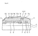
- FIG. 6 is a sectional structural view of a memory cell of an SRAM according to this embodiment.
- This embodiment is characterised in that an n ++ impurity layer 120 of a high concentration is formed in a junction portion of silicon plug 15 and interconnection layer 8a.
- a function of high concentration n ++ impurity layer 120 will be described. If a p type impurity layer is joined to an n type impurity layer having a normal concentration, a pn junction is produced.
- N ++ impurity layer 120 of a high concentration is formed by an ion implantation method, as described below.
- p type impurity is implanted in a main surface of a silicon substrate 1 using, for example, an ion implantation method. Subsequently, implanted p type impurity is diffused to the depth of about 2 - 3 ⁇ m from the main surface of substrate 1 by heat treatment to form a p well 2.
- a field oxide film 4 and p + isolation layer 3 are formed on a prescribed region of a surface of p well 2 for isolation.
- Oxide films 5 of 12nm - 15nm thickness are formed on the surface of p well 2 using, for example, a thermal oxidation method. Oxide films 5 form gate oxide films 5,5 of MOS transistors 20a, 22b.
- a polycide film formed of polycrystalline silicon 6a and refractory metal silicide 6b formed thereon is deposited on the surface of oxide films 5.
- the polycide film is patterned to a prescribed shape using a photolithography method and an etching method to form gate electrodes 6, 6 of MOS transistors 20a, 22b.
- N type impurity ions of a dose of 4x10 15 ions/cm 2 are implanted into p well 2 by an ion implantation method using the patterned gate electrodes 6 as masks. Subsequently, heat treatment is performed to activate impurity ions implanted into p well 2.
- n + source/drain regions 7 of four MOS transistors 20a, 20b, 22a, 22b are formed.
- n channel MOS drive transistors 20a, 20b and n channel MOS transfer transistors 22a, 22b are formed.
- a BPSG (BoroPhospho Silicate Glass) film is deposited on the whole surface of silicon substrate 1 using, for example, an atmospheric pressure CVD (Chemical Vapour Deposition) method.
- the BPSG is softened and reflowed by heat treatment, so that the surface of the BPSG film is planarized.
- an interlevel insulating layer 9 having a planarized surface is formed.
- An opening 16 for direct contact is formed in interlevel insulating layer 9 using a photolithography method and an etching method.
- a reactive ion etching method is used for the etching method to form opening 16.
- a polycrystalline silicon layer 15a not doped with impurity is formed on a surface of interlevel insulating layer 9 using LPCVD (Low Pressure Chemical Vapor Deposition) method.
- Polycrystalline silicon layer 15a is deposited so thick as to fill opening 16 completely and make a surface of itself substantially flat in an upper portion of opening 16. A thickness more than a half of a maximum diameter of opening 16 is required as a standard of a thickness of polycrystalline silicon layer 15a to fill opening 16 completely.
- the polycrystalline silicon layer 15a is etched, leaving a portion of the polycrystalline silicon layer only within opening 16 using an etch back method. Isotropic etching is used for the etching. In isotropic etching, polycrystalline silicon layer 15a is isotropically etched on the surface of interlevel insulating layer 9, but in the upper portion of opening 16, it is etched flat. As a result, only in opening 16, polycrystalline silicon layer 15a remains defining thus a plug 15 of polycrystalline silicon.
- a resist pattern 17a having an opening only in the upper portion of opening 16 is formed on the surface of interlevel insulating layer 9.
- n type impurity ions 18a are implanted into silicon plug 15 to provide n type conductivity.
- the ion implantation is carried out using, for example, phosphorus (P) ions in a dose of 1.5 x 10 16 ions/cm 2 with implantation energy of 170 keV.
- P phosphorus
- using phosphorus having a large diffusion coefficient in silicon for impurities in the ion implantation is also important.
- Phosphorus having a large diffusion coefficient diffuses uniformly in the whole silicon plug 15.
- the phosphorus ions introduced into silicon plug layer 15 are activated using, for example, a rapid thermal anneal (RTA) method to form an n + silicon plug 15.
- RTA rapid thermal anneal
- heat treatment is carried out, for example, for thirty seconds at a temperature of 1100°C in nitrogen atmosphere using a lamp anneal device having a halogen lamp for a heat source.
- the reason to remove resist pattern 17a before carrying out the RTA method is that, since the main component of resist pattern 17a is organic substance, harmful substance in the organic substance should be prevented from diffusing in the semiconductor in the heat treatment of the RTA method.
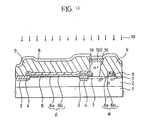
- a resist pattern 17b having the same pattern as resist pattern 17a formed in Fig.10 is formed on the surface of interlevel insulating layer 9.
- N type impurity ions 18b are implanted into the surface of n + silicon plug 15 using, for example, an ion implantation method.
- the ion implantation is carried out using arsenic in a dose of 3 x 10 15 ions/cm 2 with implantation energy of 10keV, and n ++ impurity layer 120 of a high concentration (1.5 x 10 21 /cm 3 ) is formed.
- N ++ impurity layer 120 of a high concentration is formed by implanting arsenic ions.
- arsenic Compared to, for example, phosphorus, arsenic has a smaller diffusion coefficient, so that it can be restrained from diffusing deeply into silicon plug 15 by the influence of heat treatment in the subsequent steps.
- Implantation energy of arsenic ions 18b is set low to form n ++ impurity layer 120 in a shallow region, that is, at the depth of about 30-50nm. Heat treatment is not carried out after implantation of arsenic ions 18b in order to suppress the diffusion of n ++ impurity layer 120 of a high concentration.
- a polycrystalline silicon layer 8 to which no impurities are introduced is deposited in a thickness of about 100 nm using an LPCVD method on the surfaces of interlevel insulating layer 9 and n ++ impurity layer 120 of a high concentration. Then, p type impurity ions 19 are implanted into polycrystalline silicon layer 8 in a dose of about 1 x 10 16 ions/cm 2 , and the p type impurity ions are activated in heat treatment.
- the concentration of the p type impurities introduced into polycrystalline silicon layer 8 is high (1 x 10 21 /cm 3 ). This is because a pn junction of high concentration (i.e. p ++ n ++ ) is to be formed at the junction of n ++ impurity layer 120, which has a high concentration, and polycrystalline silicon layer 8.
- polycrystalline silicon layer 8 of p type is patterned using a photolithography method and an etching method.
- a gate electrode 8b of p channel MOS thin film transistor 21b and interconnection layer 8a are formed in this step.
- a gate oxide film 13 of a thickness of about 20nm is deposited on the whole surface of interlevel insulating layer 9 using, for example, the LPCVD method. One portion of gate oxide film 13 located above opening 16 is opened.
- a thin polycrystalline silicon layer is formed with a thickness of about 10nm on the whole surface of gate oxide film 13 using, for example, the LPCVD method, and p + source/drain regions 12a, 12c and a channel region 12b of a p channel MOS thin film load transistor 21b are patterned using a photolithography method and an etching method.
- a resist is formed on regions of the polycrystalline silicon layer which are to be channel regions of p channel MOS thin film load transistors 21a, 21b.
- P type impurity ion is ion-implanted into the polycrystalline silicon layer in a dose of about 1x10 15 ions/cm 2 using the resist as a mask, so that p + source/drain regions 12a, 12c of p channel MOS thin film load transistors 21a, 21b are formed.
- a silicon plug is embedded within a contact hole and an upper interconnection layer is formed on a planarised layer, so that patterning precision of the interconnection layer using a photolithography method is improved and reliability of interconnection is enhanced.
- pn junction p ++ n ++
- the silicon plug can be formed using a known CVD method and an etch back method, complicated manufacturing steps are not needed.
Landscapes
- Semiconductor Memories (AREA)
- Internal Circuitry In Semiconductor Integrated Circuit Devices (AREA)
- Metal-Oxide And Bipolar Metal-Oxide Semiconductor Integrated Circuits (AREA)
Claims (4)
- Gestapelte Halbleitervorrichtung mit einem ersten und einem zweiten MOS-Transistor (22b, 21b) komplementären Kanalleitungstyps auf entsprechenden unterschiedlichen Niveaus, die durch eine Zwischenniveau-Isolierschicht (9) getrennt sind, bei der ein dotierter Bereich (7) eines Leitungstyps des ersten MOS-Transistors (22b) mit einem dotierten Bereich (12a) entgegengesetzten Leitungstyps des zweiten MOS-Transistors (21b) verbunden ist durch eine Direktkontaktstruktur (8a, 15), die aus einer dotierten Polysiliziumverbindungsschicht (8a) des entgegengesetzten Leitungstyps, die auf der Zwischenniveau-Isolierschicht (9) vorgesehen und in direktem Kontakt mit dem dotierten Bereich (12a) des zweiten MOS-Transistors (21b) ist, und aus einem leitenden Stopfen (15) aus dotiertem Polysilizium des einen Leitungstyps, der sich durch die Zwischenniveau-Isolierschicht (9) erstreckt und in direktem Kontakt mit dem dotierten Bereich (7) des ersten MOS-Transistors (22b) ist, gebildet ist, bei der ein stark dotierter pn-Tunnelübergang, p++n++, an dem Übergang der dotierten Polysiliziumverbindungsschicht (8a) und des leitenden Stopfens (15) aus dotiertem Polysilizium ausgebildet ist, der leitende Stopfen (15) zwei unterschiedliche Dotierstoffe in sich aufweist, wobei ein erster Dotierstoff über seinen Körper (15) verteilt ist und ein zweiter Dotierstoff in einer Oberflächenschicht (120) desselben lokalisiert ist, was eine höhere Konzentration von Dotierstoffionen als in dem Körper desselben an dem Übergang liefert.
- Gestapelte Halbleitervorrichtung, bei der der erste Dotierstoff Phosphor und der zweite Dotierstoff Arsen ist.
- Verfahren zur Herstellung der gestapelten Halbleitervorrichtung nach Anspruch 1, das die folgenden Schritte aufweist:Liefern eines Substrates (1), das den ersten MOS-Transistor (22b) definiert in einer ersten Siliziumschicht (2) und die Zwischenniveau-Isolierschicht (9), die auf dieser vorgesehen ist, aufweist;Ausbilden einer Öffnung (16) in der Zwischenniveau-Isolierschicht (9) zum Freilegen des Bereiches (7) des einen Leitungstyps des ersten MOS-Transistors (22b);Ausbilden einer zweiten Siliziumschicht (15a) auf der Oberfläche der Zwischenniveau-Isolierschicht (9) und innerhalb der Öffnung (16);Zurückätzen der zweiten Siliziumschicht (15a) zum Entfernen des Abschnittes derselben auf der Oberfläche der Zwischenniveau-Isolierschicht (9) zum Belassen eines Stopfenabschnittes (15) derselben, der innerhalb der Öffnung (16) verbleibt;Erzeugen einer ersten Maskenschicht (17a) auf der Oberfläche der Zwischenniveau-Isolierschicht (9) mit einer Öffnung, die den Stopfenabschnitt (15) freilegt;Implantieren von Ionen eines ersten Dotierstoffs des einen Leitungstyps in den Körper des Stopfenabschnitts (15);Entfernen der ersten Maskenschicht (17a);Diffundieren der Ionen des ersten Leitungstyps überall in den Körper des Stopfenabschnittes (15) und Aktivieren der Ionen zum Erzeugen des leitenden Stopfens (15);Erzeugen einer zweiten Maskenschicht (17b) auf der Oberfläche der Zwischenniveau-Isolierschicht (9) mit einer Öffnung, die den leitenden Stopfen (15) freilegt ;Implantieren von Ionen eines zweiten Dotierstoffs des einen Leitungstyps in die Oberfläche des leitenden Stopfens (15) zum Produzieren der Schicht (120) höherer Konzentration von Dotierstoffionen in dieser;Abscheiden einer dritten Siliziumschicht (8) auf der Oberfläche der Zwischenniveau-Isolierschicht (9) und auf der Oberfläche des leitenden Stopfens (120,15);Implantieren von Dotierstoffionen des entgegengesetzten Leitungstyps in die dritte Siliziumschicht (8) und Aktivieren der Ionen durch eine thermische Behandlung, um derart die dotierte Polysilizium-Verbindungsschicht (8a) und an dem Übergang derselben mit dem leitenden Stopfen (120, 15) den stark dotierten pn-Tunnelübergang, p++n++, zu erzeugen; undErzeugen des zweiten MOS-Transistors (21b) vom komplementären Kanalleitungstyp mit dem dotierten Bereich (12a) des entgegengesetzten Leitungstyps in Kontakt mit der dotierten Polysiliziumverbindungsschicht (8a).
- Verfahren nach Anspruch 3, bei dem der erste Dotierstoff Phosphor und der zweite Dotierstoff Arsen ist.
Applications Claiming Priority (4)
| Application Number | Priority Date | Filing Date | Title |
|---|---|---|---|
| JP50954/91 | 1991-03-15 | ||
| JP5095491 | 1991-03-15 | ||
| JP5222/92 | 1992-01-14 | ||
| JP4005222A JPH0541378A (ja) | 1991-03-15 | 1992-01-14 | 半導体装置およびその製造方法 |
Publications (3)
| Publication Number | Publication Date |
|---|---|
| EP0503904A2 EP0503904A2 (de) | 1992-09-16 |
| EP0503904A3 EP0503904A3 (en) | 1992-11-19 |
| EP0503904B1 true EP0503904B1 (de) | 1998-09-30 |
Family
ID=26339127
Family Applications (1)
| Application Number | Title | Priority Date | Filing Date |
|---|---|---|---|
| EP92302045A Expired - Lifetime EP0503904B1 (de) | 1991-03-15 | 1992-03-11 | Gestapelte CMOS Halbleitervorrichtung und Verfahren zu ihrer Herstellung |
Country Status (4)
| Country | Link |
|---|---|
| US (3) | US5475240A (de) |
| EP (1) | EP0503904B1 (de) |
| JP (1) | JPH0541378A (de) |
| DE (1) | DE69227138T2 (de) |
Families Citing this family (38)
| Publication number | Priority date | Publication date | Assignee | Title |
|---|---|---|---|---|
| US5432129A (en) * | 1993-04-29 | 1995-07-11 | Sgs-Thomson Microelectronics, Inc. | Method of forming low resistance contacts at the junction between regions having different conductivity types |
| JP3256048B2 (ja) * | 1993-09-20 | 2002-02-12 | 富士通株式会社 | 半導体装置及びその製造方法 |
| US5956615A (en) * | 1994-05-31 | 1999-09-21 | Stmicroelectronics, Inc. | Method of forming a metal contact to landing pad structure in an integrated circuit |
| US5702979A (en) * | 1994-05-31 | 1997-12-30 | Sgs-Thomson Microelectronics, Inc. | Method of forming a landing pad structure in an integrated circuit |
| US5945738A (en) * | 1994-05-31 | 1999-08-31 | Stmicroelectronics, Inc. | Dual landing pad structure in an integrated circuit |
| US5796673A (en) * | 1994-10-06 | 1998-08-18 | Mosaid Technologies Incorporated | Delay locked loop implementation in a synchronous dynamic random access memory |
| US5705427A (en) * | 1994-12-22 | 1998-01-06 | Sgs-Thomson Microelectronics, Inc. | Method of forming a landing pad structure in an integrated circuit |
| JP4156044B2 (ja) * | 1994-12-22 | 2008-09-24 | エスティーマイクロエレクトロニクス,インコーポレイテッド | 集積回路におけるランディングパッド構成体の製造方法 |
| JPH08181205A (ja) * | 1994-12-26 | 1996-07-12 | Mitsubishi Electric Corp | 半導体装置の配線構造およびその製造方法 |
| US5973369A (en) * | 1997-03-11 | 1999-10-26 | Nec Corporation | SRAM having P-channel TFT as load element with less series-connected high resistance |
| JP3443219B2 (ja) * | 1995-11-14 | 2003-09-02 | 株式会社日立製作所 | 半導体集積回路装置およびその製造方法 |
| KR0167274B1 (ko) * | 1995-12-07 | 1998-12-15 | 문정환 | 씨모스 아날로그 반도체장치와 그 제조방법 |
| JP3104609B2 (ja) * | 1996-02-09 | 2000-10-30 | 日本電気株式会社 | 半導体装置およびその製造方法 |
| US5869391A (en) * | 1996-08-20 | 1999-02-09 | Micron Technology, Inc. | Semiconductor method of making electrical connection between an electrically conductive line and a node location, and integrated circuitry |
| JPH1070266A (ja) * | 1996-08-26 | 1998-03-10 | Nec Corp | 半導体装置およびその製造方法 |
| JPH10150198A (ja) * | 1996-11-18 | 1998-06-02 | Mitsubishi Electric Corp | 薄膜トランジスタおよびその製造方法 |
| JP2988413B2 (ja) * | 1997-02-20 | 1999-12-13 | 日本電気株式会社 | 半導体装置及びその製造方法 |
| JPH10242299A (ja) | 1997-02-27 | 1998-09-11 | Nec Corp | 半導体記憶装置及びその製造方法 |
| US5998257A (en) * | 1997-03-13 | 1999-12-07 | Micron Technology, Inc. | Semiconductor processing methods of forming integrated circuitry memory devices, methods of forming capacitor containers, methods of making electrical connection to circuit nodes and related integrated circuitry |
| US5854127A (en) * | 1997-03-13 | 1998-12-29 | Micron Technology, Inc. | Method of forming a contact landing pad |
| TW333687B (en) * | 1997-04-02 | 1998-06-11 | United Microelectronics Corp | The method for forming poly-via in driver transistor |
| KR100418436B1 (ko) * | 1997-06-27 | 2004-05-03 | 주식회사 하이닉스반도체 | 반도체 소자의 콘택 형성 방법 |
| KR100451042B1 (ko) * | 1997-06-27 | 2004-12-03 | 주식회사 하이닉스반도체 | 반도체소자의콘택형성방법 |
| US6380026B2 (en) * | 1997-08-22 | 2002-04-30 | Micron Technology, Inc. | Processing methods of forming integrated circuitry memory devices, methods of forming DRAM arrays, and related semiconductor masks |
| JP3807836B2 (ja) | 1997-11-28 | 2006-08-09 | 株式会社ルネサステクノロジ | 半導体装置および半導体装置の製造方法 |
| US5888887A (en) * | 1997-12-15 | 1999-03-30 | Chartered Semiconductor Manufacturing, Ltd. | Trenchless buried contact process technology |
| JP2002261277A (ja) | 2001-03-06 | 2002-09-13 | Toshiba Corp | 半導体装置及びその製造方法 |
| KR100455724B1 (ko) * | 2001-10-08 | 2004-11-12 | 주식회사 하이닉스반도체 | 반도체소자의 플러그 형성방법 |
| JP4427259B2 (ja) * | 2003-02-28 | 2010-03-03 | 株式会社東芝 | 半導体装置及びその製造方法 |
| KR100615085B1 (ko) * | 2004-01-12 | 2006-08-22 | 삼성전자주식회사 | 노드 콘택 구조체들, 이를 채택하는 반도체소자들, 이를채택하는 에스램 셀들 및 이를 제조하는 방법들 |
| DE102004024659B4 (de) * | 2004-05-18 | 2014-10-02 | Infineon Technologies Ag | Halbleiterbauteil |
| KR100595855B1 (ko) * | 2004-12-29 | 2006-06-30 | 동부일렉트로닉스 주식회사 | 알루미늄 증착 콘택트 형성 방법 |
| KR100684894B1 (ko) * | 2005-04-18 | 2007-02-20 | 삼성전자주식회사 | 적층된 트랜지스터들을 구비하는 반도체 장치의 형성 방법 |
| US8183087B2 (en) | 2008-09-09 | 2012-05-22 | Stats Chippac, Ltd. | Semiconductor device and method of forming a fan-out structure with integrated passive device and discrete component |
| JP5068296B2 (ja) * | 2009-09-25 | 2012-11-07 | ルネサスエレクトロニクス株式会社 | 半導体記憶装置の製造方法 |
| KR101169167B1 (ko) * | 2010-10-25 | 2012-07-30 | 에스케이하이닉스 주식회사 | 반도체 소자 및 그 형성 방법 |
| JPWO2013190759A1 (ja) * | 2012-06-21 | 2016-02-08 | パナソニックIpマネジメント株式会社 | 固体撮像素子及びその製造方法 |
| US20160276156A1 (en) * | 2015-03-16 | 2016-09-22 | Taiwan Semiconductor Manufacturing Company Ltd. | Semiconductor device and manufacturing process thereof |
Family Cites Families (24)
| Publication number | Priority date | Publication date | Assignee | Title |
|---|---|---|---|---|
| US4785341A (en) * | 1979-06-29 | 1988-11-15 | International Business Machines Corporation | Interconnection of opposite conductivity type semiconductor regions |
| JPS5640269A (en) * | 1979-09-11 | 1981-04-16 | Toshiba Corp | Preparation of semiconductor device |
| JPS5846193B2 (ja) * | 1980-07-15 | 1983-10-14 | 株式会社東芝 | 半導体装置 |
| JPS57204171A (en) * | 1981-06-10 | 1982-12-14 | Mitsubishi Electric Corp | Semiconductor device |
| JPS60186051A (ja) * | 1984-03-05 | 1985-09-21 | Hitachi Ltd | Cmos半導体装置およびその製造方法 |
| EP0164829B1 (de) * | 1984-04-19 | 1988-09-28 | Nippon Telegraph And Telephone Corporation | Halbleiterspeicherbauelement und Verfahren zur Herstellung |
| US4710897A (en) * | 1984-04-27 | 1987-12-01 | Kabushiki Kaisha Toshiba | Semiconductor memory device comprising six-transistor memory cells |
| JPS616855A (ja) * | 1984-06-20 | 1986-01-13 | Nec Corp | 相補型mos半導体装置 |
| JPS6140133A (ja) * | 1984-07-31 | 1986-02-26 | Shiro Kanao | 可撓性ホ−スの製造方法 |
| JPS62132317A (ja) * | 1985-12-04 | 1987-06-15 | Mitsubishi Electric Corp | 半導体装置の電極形成方法 |
| JPS62274659A (ja) * | 1986-05-22 | 1987-11-28 | Mitsubishi Electric Corp | 半導体装置 |
| US4829018A (en) * | 1986-06-27 | 1989-05-09 | Wahlstrom Sven E | Multilevel integrated circuits employing fused oxide layers |
| US4727045A (en) * | 1986-07-30 | 1988-02-23 | Advanced Micro Devices, Inc. | Plugged poly silicon resistor load for static random access memory cells |
| ATE75340T1 (de) * | 1987-01-28 | 1992-05-15 | Advanced Micro Devices Inc | Statische ram-zellen mit vier transistoren. |
| US4966865A (en) * | 1987-02-05 | 1990-10-30 | Texas Instruments Incorporated | Method for planarization of a semiconductor device prior to metallization |
| JPH0215620A (ja) * | 1988-07-01 | 1990-01-19 | Nec Corp | 半導体装置の製造方法 |
| JP2753581B2 (ja) * | 1988-09-07 | 1998-05-20 | 株式会社東芝 | ファクシミリ装置 |
| JPH0273666A (ja) * | 1988-09-08 | 1990-03-13 | Sony Corp | 半導体メモリ装置 |
| JP2623812B2 (ja) * | 1989-01-25 | 1997-06-25 | 日本電気株式会社 | 半導体装置の製造方法 |
| JPH07109863B2 (ja) * | 1989-04-13 | 1995-11-22 | 日本電気株式会社 | 能動層2層積層記憶素子 |
| US5151376A (en) * | 1990-05-31 | 1992-09-29 | Sgs-Thomson Microelectronics, Inc. | Method of making polycrystalline silicon resistors for integrated circuits |
| US5041884A (en) * | 1990-10-11 | 1991-08-20 | Mitsubishi Denki Kabushiki Kaisha | Multilayer semiconductor integrated circuit |
| US5198683A (en) * | 1991-05-03 | 1993-03-30 | Motorola, Inc. | Integrated circuit memory device and structural layout thereof |
| US5232865A (en) * | 1991-07-24 | 1993-08-03 | Micron Technology, Inc. | Method of fabricating vertically integrated oxygen-implanted polysilicon resistor |
-
1992
- 1992-01-14 JP JP4005222A patent/JPH0541378A/ja not_active Withdrawn
- 1992-03-11 EP EP92302045A patent/EP0503904B1/de not_active Expired - Lifetime
- 1992-03-11 DE DE69227138T patent/DE69227138T2/de not_active Expired - Fee Related
-
1994
- 1994-08-19 US US08/293,771 patent/US5475240A/en not_active Expired - Fee Related
-
1995
- 1995-11-07 US US08/554,508 patent/US5581093A/en not_active Expired - Fee Related
- 1995-11-07 US US08/554,507 patent/US5654239A/en not_active Expired - Fee Related
Also Published As
| Publication number | Publication date |
|---|---|
| US5654239A (en) | 1997-08-05 |
| DE69227138D1 (de) | 1998-11-05 |
| EP0503904A2 (de) | 1992-09-16 |
| US5475240A (en) | 1995-12-12 |
| US5581093A (en) | 1996-12-03 |
| DE69227138T2 (de) | 1999-04-01 |
| EP0503904A3 (en) | 1992-11-19 |
| JPH0541378A (ja) | 1993-02-19 |
Similar Documents
| Publication | Publication Date | Title |
|---|---|---|
| EP0503904B1 (de) | Gestapelte CMOS Halbleitervorrichtung und Verfahren zu ihrer Herstellung | |
| JP2520556B2 (ja) | 薄膜疑似プレ―ナpfetデバイスを作製する方法 | |
| US5547893A (en) | method for fabricating an embedded vertical bipolar transistor and a memory cell | |
| US5334862A (en) | Thin film transistor (TFT) loads formed in recessed plugs | |
| US6222214B1 (en) | Plug structure and process for forming stacked contacts and metal contacts on static random access memory thin film transistors | |
| US5071784A (en) | Method of making a semiconductor memory device | |
| US6242297B1 (en) | Semiconductor device having an improved interconnection and method for fabricating the same | |
| JP2646508B2 (ja) | スタテイツク・ライト・リード・メモリにおける交差結合の製作方法 | |
| JPH06151772A (ja) | 二重垂直チャネルを有するsram及びその製造方法 | |
| US5777920A (en) | Semiconductor memory device and method of manufacturing the same | |
| US5497022A (en) | Semiconductor device and a method of manufacturing thereof | |
| KR0148404B1 (ko) | 부하로 동작하는 박막 트랜지스터를 가진 정적 램 | |
| US5945715A (en) | Semiconductor memory device having a memory cell region and a peripheral circuit region and method of manufacturing the same | |
| JP2000277629A (ja) | 半導体記憶装置及びその製造方法 | |
| US6690071B2 (en) | Semiconductor device using junction leak current | |
| US5917247A (en) | Static type memory cell structure with parasitic capacitor | |
| US5106782A (en) | Method of manufacturing a semiconductor device | |
| US5926698A (en) | Semiconductor memory device and method of fabricating the same | |
| JP2908146B2 (ja) | 半導体装置およびその製造方法 | |
| KR0170311B1 (ko) | 스태틱 랜덤 억세스 메모리 및 그 제조방법 | |
| JP2959129B2 (ja) | Sram装置およびその製造方法 | |
| US6001674A (en) | Method of eliminating buried contact trench in SRAM devices | |
| KR100207809B1 (ko) | 반도체 장치 및 그의 제조방법 | |
| JP3354333B2 (ja) | 半導体記憶装置 | |
| JP2523645B2 (ja) | 半導体記憶装置およびその製造方法 |
Legal Events
| Date | Code | Title | Description |
|---|---|---|---|
| PUAI | Public reference made under article 153(3) epc to a published international application that has entered the european phase |
Free format text: ORIGINAL CODE: 0009012 |
|
| AK | Designated contracting states |
Kind code of ref document: A2 Designated state(s): DE FR NL |
|
| PUAL | Search report despatched |
Free format text: ORIGINAL CODE: 0009013 |
|
| AK | Designated contracting states |
Kind code of ref document: A3 Designated state(s): DE FR NL |
|
| 17P | Request for examination filed |
Effective date: 19930514 |
|
| R17P | Request for examination filed (corrected) |
Effective date: 19930514 |
|
| 17Q | First examination report despatched |
Effective date: 19941128 |
|
| GRAG | Despatch of communication of intention to grant |
Free format text: ORIGINAL CODE: EPIDOS AGRA |
|
| GRAG | Despatch of communication of intention to grant |
Free format text: ORIGINAL CODE: EPIDOS AGRA |
|
| GRAG | Despatch of communication of intention to grant |
Free format text: ORIGINAL CODE: EPIDOS AGRA |
|
| GRAH | Despatch of communication of intention to grant a patent |
Free format text: ORIGINAL CODE: EPIDOS IGRA |
|
| GRAH | Despatch of communication of intention to grant a patent |
Free format text: ORIGINAL CODE: EPIDOS IGRA |
|
| GRAA | (expected) grant |
Free format text: ORIGINAL CODE: 0009210 |
|
| AK | Designated contracting states |
Kind code of ref document: B1 Designated state(s): DE FR NL |
|
| REF | Corresponds to: |
Ref document number: 69227138 Country of ref document: DE Date of ref document: 19981105 |
|
| ET | Fr: translation filed | ||
| PLBE | No opposition filed within time limit |
Free format text: ORIGINAL CODE: 0009261 |
|
| 26N | No opposition filed | ||
| PGFP | Annual fee paid to national office [announced via postgrant information from national office to epo] |
Ref country code: DE Payment date: 20000306 Year of fee payment: 9 |
|
| PGFP | Annual fee paid to national office [announced via postgrant information from national office to epo] |
Ref country code: FR Payment date: 20000310 Year of fee payment: 9 |
|
| PGFP | Annual fee paid to national office [announced via postgrant information from national office to epo] |
Ref country code: NL Payment date: 20000330 Year of fee payment: 9 |
|
| PG25 | Lapsed in a contracting state [announced via postgrant information from national office to epo] |
Ref country code: NL Free format text: LAPSE BECAUSE OF NON-PAYMENT OF DUE FEES Effective date: 20011001 |
|
| PG25 | Lapsed in a contracting state [announced via postgrant information from national office to epo] |
Ref country code: FR Free format text: LAPSE BECAUSE OF NON-PAYMENT OF DUE FEES Effective date: 20011130 |
|
| NLV4 | Nl: lapsed or anulled due to non-payment of the annual fee |
Effective date: 20011001 |
|
| REG | Reference to a national code |
Ref country code: FR Ref legal event code: ST |
|
| PG25 | Lapsed in a contracting state [announced via postgrant information from national office to epo] |
Ref country code: DE Free format text: LAPSE BECAUSE OF NON-PAYMENT OF DUE FEES Effective date: 20020101 |