EP0506416A2 - Verfahren zur Herstellung eines Substrates von SOI-Type mit einer monokristallinen Schicht aus Silizium auf einer isolierenden Schicht - Google Patents
Verfahren zur Herstellung eines Substrates von SOI-Type mit einer monokristallinen Schicht aus Silizium auf einer isolierenden Schicht Download PDFInfo
- Publication number
- EP0506416A2 EP0506416A2 EP92302654A EP92302654A EP0506416A2 EP 0506416 A2 EP0506416 A2 EP 0506416A2 EP 92302654 A EP92302654 A EP 92302654A EP 92302654 A EP92302654 A EP 92302654A EP 0506416 A2 EP0506416 A2 EP 0506416A2
- Authority
- EP
- European Patent Office
- Prior art keywords
- temperature
- silicon
- silicon substrate
- rise rate
- substrate
- Prior art date
- Legal status (The legal status is an assumption and is not a legal conclusion. Google has not performed a legal analysis and makes no representation as to the accuracy of the status listed.)
- Granted
Links
Images



Classifications
-
- H—ELECTRICITY
- H10—SEMICONDUCTOR DEVICES; ELECTRIC SOLID-STATE DEVICES NOT OTHERWISE PROVIDED FOR
- H10P—GENERIC PROCESSES OR APPARATUS FOR THE MANUFACTURE OR TREATMENT OF DEVICES COVERED BY CLASS H10
- H10P30/00—Ion implantation into wafers, substrates or parts of devices
- H10P30/20—Ion implantation into wafers, substrates or parts of devices into semiconductor materials, e.g. for doping
- H10P30/208—Ion implantation into wafers, substrates or parts of devices into semiconductor materials, e.g. for doping of electrically inactive species
- H10P30/209—Ion implantation into wafers, substrates or parts of devices into semiconductor materials, e.g. for doping of electrically inactive species in silicon to make buried insulating layers
-
- H—ELECTRICITY
- H10—SEMICONDUCTOR DEVICES; ELECTRIC SOLID-STATE DEVICES NOT OTHERWISE PROVIDED FOR
- H10P—GENERIC PROCESSES OR APPARATUS FOR THE MANUFACTURE OR TREATMENT OF DEVICES COVERED BY CLASS H10
- H10P90/00—Preparation of wafers not covered by a single main group of this subclass, e.g. wafer reinforcement
- H10P90/19—Preparing inhomogeneous wafers
- H10P90/1904—Preparing vertically inhomogeneous wafers
- H10P90/1906—Preparing SOI wafers
- H10P90/1908—Preparing SOI wafers using silicon implanted buried insulating layers, e.g. oxide layers [SIMOX]
-
- H—ELECTRICITY
- H10—SEMICONDUCTOR DEVICES; ELECTRIC SOLID-STATE DEVICES NOT OTHERWISE PROVIDED FOR
- H10P—GENERIC PROCESSES OR APPARATUS FOR THE MANUFACTURE OR TREATMENT OF DEVICES COVERED BY CLASS H10
- H10P95/00—Generic processes or apparatus for manufacture or treatments not covered by the other groups of this subclass
- H10P95/90—Thermal treatments, e.g. annealing or sintering
-
- H—ELECTRICITY
- H10—SEMICONDUCTOR DEVICES; ELECTRIC SOLID-STATE DEVICES NOT OTHERWISE PROVIDED FOR
- H10W—GENERIC PACKAGES, INTERCONNECTIONS, CONNECTORS OR OTHER CONSTRUCTIONAL DETAILS OF DEVICES COVERED BY CLASS H10
- H10W10/00—Isolation regions in semiconductor bodies between components of integrated devices
- H10W10/10—Isolation regions comprising dielectric materials
- H10W10/181—Semiconductor-on-insulator [SOI] isolation regions, e.g. buried oxide regions of SOI wafers
Definitions
- the present invention relates to a method for manufacturing an SOI (Silicon on Insulator) substrate which has a monocrystal silicon layer on an insulating film and has attracted the attention as a substrate of a VLSI in the future, and particularly to a method, which enables manufacturing of the SOI substrate having a low defect density of the monocrystal silicon layer.
- SOI Silicon on Insulator
- Figs. 9A - 9C are cross sectional views, which show an example of a conventional manufacturing method of the SOI substrate, and specifically an SIMOX (Separation by Implanted Oxygen) method for manufacturing the SOI substrate in accordance with the steps.
- SIMOX Separatation by Implanted Oxygen
- oxygen is ion-implanted at an implantation dose of about 2 x 10¹⁸/cm2 into a silicon substrate by an accelerating voltage of about 200keV, and then annealing or heat treatment is sufficiently applied to the substrate in gas mixture of Ar/O2 or N2/O2 at a high temperature not less than 1300°C, so that a silicon oxide layer (SiO2 film), i.e., a buried insulating film is directly formed in the silicon substrate.
- SiO2 film silicon oxide layer
- a silicon substrate 1 shown in Fig. 9A is heated to 500 - 600°C.
- oxygen ion 2 is implanted into silicon substrate 1 at the implantation dose of about 2.0 x 10¹⁸/cm2 by the accelerating voltage of 200keV.
- Silicon substrate 1 and the oxygen which is directly implanted thereinto react on each other to form a buried silicon oxide film 3.
- Fig. 12 shows a density profile of oxygen in the silicon substrate in the cases that oxygen ion is implanted at various implantation doses by the accelerating voltage of 200keV.
- the oxygen shows a Guassian distribution in the silicon substrate.
- the oxygen ion implantation dose is higher than a critical implantation dose of 1.35 x 10¹⁸/cm2, an oxygen concentration near an implantation peak exceeds a stoichiometric concentration of SiO2, i.e., 4.4 x 10²²/cm3, so that an SiO2 film is formed.
- Residual silicon layer 4 is damaged by the ion implantation, and also has a high oxygen concentration and the above described defect. Therefore, layer 4 requires heat treatment, for example, in an atmosphere of Ar/O2 at a temperature of 1300°C for 5 hours, in order to restore crystallinity of the residual silicon layer 4.
- a conventional heat treatment step as shown in Fig. 10, silicon substrate 1 is heated at a constant temperature-rise rate until it reaches a holding temperature (1300°C).
- Fig. 11 shows a time chart of these typical heat treatment step. In a flow of the typical heat treatment, the temperature is raised at the temperature-rise rate of, e.g., 20°C/min.
- r o (2 ⁇ / ⁇ H v ) ⁇ (T E /(T E - T))
- Threading dislocation 6 remains in monocrystal silicon layer 5 to deteriorate the crystal quality thereof.
- a mechanism of formation of such dislocation is disclosed, for example, in J. Stoemenos et al., J. Appl. Phys., Vol. 69, NO. 2, 15 January 1991, pp. 793 - 802.
- the density of the threading dislocation depends on conditions for implanting the oxygen ion. As shown in Fig. 13, the higher implantation dose of oxygen ion and the lower accelerating voltage tend to increase the dislocation density.
- a multiple ion implanting (multi-step implanting) method utilizing the correlativity between the implantation dose of oxygen ion and the dislocation density (defect density) has been developed and reported in D. Hill et al., J. Appl. Phys., Vol. 63, No. 10, 15 May 1988, pp. 4933-4936.
- the oxygen ion is implanted-at-the implantation dose (in a range from 0.5 to 1 x 10¹⁸/cm2) lower than the conventional dose in order to reduce the dislocation density, and then annealing is conducted for restoring crystallinity and growing the SiO2. Thereafter, the implantation of oxygen ion and the annealling are repeated for few times in order to obtain a predetermined implantation dose.
- This method can produce the good SOI substrate, in which the interface between the monocrystal silicon layer and the silicon oxide film is very steep, and also the dislocation density of the monocrystal silicon layer is lower than 103/cm2. This method, however, requires complicated processes, and thus is not suitable to a commercial mass production.
- the threading dislocation remains in the SOI layer at a density of about 108/cm2. If the threading dislocation remains, and thus MOS transistors are formed in the SOI layer having deteriorated crystal quality, the defect and/or impurity are captured into the gate oxide film when the gate oxide film is formed, which reduces a resistance against electric field of the gate oxide film. Also the defect existing in the depleted layer causes a generation current, which increases a power consumption. As described above, if the MOS transistors are formed in the SOI layer containing the residual threading dislocation, characteristics of the device deteriorate.
- the multiple ion implanting method provides the good SOI substrate having the low dislocation density, it requires the complicated processes, and is not suitable to the commercial mass production.
- An object of the invention is to manufacture an SOI substrate having a low defect density of a monocrystal silicon layer (SOI layer).
- Another object of the invention is to provide a manufacturing method of an SOI substrate, which can improve crystallinity of an SOI layer by a simple process.
- Still another object of the invention is to provide a manufacturing method of an SOI substrate, which prevents rise of dislocation to a surface of an SOI layer in a heat treatment step.
- Yet another object of the invention is to provide a manufacturing method of an SOI substrate, in which a generating rate of interstitial silicon is suppressed in a heat treatment step.
- a manufacturing method of an SOI substrate oxygen ion is implanted into a silicon substrate, so that a silicon oxide layer is formed under a silicon surface layer while remaining the silicon surface layer on a main surface of the silicon substrate. While maintaining a state in which silicon oxide particles are formed and remained in the silicon surface layer, the silicon substrate is heated to a predetermined temperature not less than 1300°C. The silicon substrate is held at the predetermined temperature for a predetermined time, whereby crystallinity of the silicon surface layer is restored.
- the step, in which the silicon substrate is heated to the predetermined temperature not less than 1300°C is conducted by a step, in which the silicon substrate is heated to a first temperature in a range from 900°C to 1100°C at a first temperature-rise rate, and a step, in which the silicon substrate is heated from the first temperature to a second temperature not less than 1300°C at a second temperature-rise rate lower than the first temperature-rise rate.
- the step, in which the silicon substrate is heated to the predetermined temperature not less than 1300°C includes a step in which the silicon substrate is held at the first temperature for a constant time.
- the silicon substrate is heated while remaining the silicon oxide particles in the silicon surface layer. Therefore, the silicon oxide particles formed and remaining in the silicon surface layer prevent dislocation from rising to and extending in a surface of the silicon surface layer by their pinning effect. This can prevent the dislocation from rising to the surface of the SOI layer (monocrystal silicon layer). Owing to the pinning effect described above, the existence of the silicon oxide particles prevents multiplication of the dislocation and stabilizes the same. Thereby, the dislocation density of the SOI layer can be remarkably reduced.
- oxygen ion is implanted into a silicon substrate, so that a silicon oxide layer is formed under a silicon surface layer while remaining the silicon surface layer on a main surface of the silicon substrate.
- the silicon substrate is heated to a first temperature at a first mean temperature-rise rate.
- the silicon substrate is heated from the first temperature to a second temperature not less than 1300°C at a second mean temperature-rise rate lower than the first mean temperature-rise rate.
- the silicon substrate is held at the second temperature for a predetermined time, whereby crystallinity of the silicon surface layer is restored.
- the first temperature is 1050°C
- the second temperature is 1300°C.
- the first mean temperature-rise rate is 20°C/min.
- the second mean temperature-rise rate is not more than 1°C/min..
- the silicon substrate is heated to the first temperature at the first mean temperature-rise rate, and is heated from the first temperature to a final heat treatment temperature, i.e., the second temperature not less than 1300°C at the lower second mean temperature-rise rate. Therefore, a rate of generation of interstitial silicon per a unit time can be suppressed. This results in reduction of a remaining density of the interstitial silicon in the SOI layer (monocrystal silicon layer) thus obtained. Thereby, the dislocation density of SOI layer can be remarkably reduced.
- the rise of the dislocation to the SOI layer surface can be prevented by the pinning effect of the residual silicon oxide particles, which are formed in the heating step of the silicon substrate after the implantation of oxygen ion. Further, the generating rate of the interstitial silicon per a unit time can be suppressed in the above heating step. Accordingly, the SOI substrate having the remarkably reduced dislocation density and the improved crystallinity can be obtained.
- a step for implanting oxygen ion is the same as the conventional step. That; is a silicon oxide film is formed by reaction of a silicon substrate and oxygen directly implanted into the silicon substrate.
- an annealing or heat treatment step is conducted to restore crystallinity of the silicon oxide film and a silicon surface layer (silicon crystal) formed thereon.
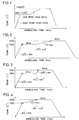
- the heat treatment step is conducted, using the heating steps in two stages, as shown in Fig. 1.
- the silicon substrate is heated at a constant temperature-rise rate, and is held for few hours at a constant temperature in a range from 900°C to 1100°C.
- the silicon substrate is heated at a temperature-rise rate, which is lower than that in the heating step at the first stage, to a final heat treatment temperature not less than 1300°C.
- the silicon substrate is held at this final heat treatment temperature for few hours, and then is cooled in a furnace.
- the silicon substrate is heated at the temperature-rise rate of 20°C/min., and is held at 1050°C for six hours in the first heating step.
- the silicon substrate is heated at the temperature-rise rate of 1°C/min., and is held at 1300°C for six hours.
- the silicon substrate is cooled in the furnace for about two hours nearly to a room temperature.
- Atmosphere in the furnace accommodating the silicon substrate contains argon (Ar) and a very small amount of oxygen (O2) mixed therein.
- the temperature-rise rate in the second heating step shown in Fig. 2 is lower than the temperature-rise rate in the first heating step.
- the second mean temperature-rise rate shown in Fig. 2 is lower than the first mean temperature-rise rate.
- the above conditions are also satisfied by another example of the heating steps shown in Fig. 3.
- the mean temperature-rise rate in the first heating step shown in Fig. 3 is 20°C/min.
- the effect of the invention can be achieved only if the mean temperature-rise rate in the second heating step is smaller than the mean temperature-rise rate in the first heating step.
- the silicon substrate is heated at the temperature-rise rate of 20°C/min. in the first heating step, and the process advances, without holding 1050°C, to the second heating step, in which the substrate is heated at the temperaturerise rate of 1°C/min.. Then, it is held at 1300°C for six hours.
- the effect of the invention can be achieved, even if the silicon substrate is not held at a constant temperature through the intermediate stage in the heating step.
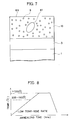
- a monocrystal silicon substrate 1 shown in Fig. 5A is heated to 500°C - 600°C.
- oxygen ion 2 is implanted into silicon substrate 1, for example, at the implantation dose of 2.0 x 10¹⁸/cm2 by the accelerating voltage of 200keV.
- the oxygen directly implanted into silicon substrate 1 reacts on silicon substrate 1 to form a silicon oxide film 3.
- Residual silicon layer 4 is formed on a silicon oxide film 3.
- the substrate is held at the intermediate stage in the heating step for few hours, or the temperature-rise rate is lowered, whereby silicon oxide particles 9, i.e., fine oxygen precipitate having a particle diameter of about tens angstroms is formed in a whole interior of an SOI layer 10, as shown in Fig. 5C.
- silicon oxide particles 9 i.e., fine oxygen precipitate having a particle diameter of about tens angstroms is formed in a whole interior of an SOI layer 10, as shown in Fig. 5C.
- Existence of silicon oxide particles 9 brings about the pinning effect, by which dislocation near the interface between silicon oxide film 3 and SOI layer 10 is suppressed from rising to the surface of SOI layer 10. If the dislocation reached the surface of SOI layer 10, it would be difficult to remove the same by any processing applied thereafter. Therefore, the pinning effect has an important part in reducing the dislocation density.
- the silicon and oxygen are not sufficiently rearranged. Therefore, the heat treatment at the high temperature is required so as to obtain the silicon oxide layer having the desired steep interface and the SOI layer excluding the defect such as dislocation and precipitate. Since the reaction by which the silicon oxide layer is formed is most remarkable in the high temperature region, it is important to suppress the rise of the dislocation in the high temperature region for preventing the formation of the threading dislocation. In this embodiment, the pinning effect of the silicon oxide particles, i.e., the oxygen precipitate formed in the first heating step suppresses the rise of the dislocation in the high temperature region.
- the temperature-rise rate were high, the critical radius would increase at a rate higher than a growing rate of the silicon oxide particles, so that nearly all silicon oxide particles, i.e., the precipitate near the surface would dissolve.
- the generating rate per a unit time of the interstitial silicon which generates during the rise of the temperature depends on the temperature-rise rate. If the temperature-rise rate were excessively high, a large mount of interstitial silicon would generate, and the dislocation would generate due to the mutual coupling of the interstitial silicon near the surface and the growth.
- the temperature is raised from a value in the intermediate stage to a value in the high temperature region at the temperature-rise rate which does not cause the melting of the silicon oxide particles deposited and grown in the intermediate stage, in order to reduce the dislocation density.
- the silicon oxide particles, i.e., the precipitate remained in the temperature rising step can be completely melted in the heat treatment conducted at the temperature above 1300°C for few hours, and thus the steep interface between the silicon oxide layer and the SOI layer can be obtained.
- the SOI layer 11 having the reduced dislocation density is formed, as shown in Fig. 5D.
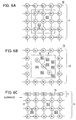
- the generating rate per a unit time of interstitial silicon 8 thus generated depends on the temperature-rise rate, and increases as the temperature-rise rate increases. However, as shown in Fig. 6C, a part of interstitial silicon 8 is absorbed into the surface of SOI layer 11. That is; a part of interstitial silicon 8 escapes to the surface of SOI layer 11, and is captured, as epitaxial growth silicon 14, into the lattice silicon to form an epitaxial growth layer 7. In this case, if the generating rate of interstitial silicon 8 were higher than the rate of the epitaxial growth caused on the surface of SOI layer 11, the interstitial silicon would mutually couple to form cluster, and might further grow to form a new surface in the silicon crystal, resulting in crystal defect such as dislocation.
- the generating rate per a unit time of the interstitial silicon is reduced so as to prevent or minimize the generation of the crystal defect.
- a method for reducing the rate of the temperature-rise from the intermediate stage to the high temperature region is employed. This reduces the residual density of the interstitial silicon in the SOI layer, and thus can reduce the dislocation density.
- silicon substrate 1 isheated while remaining silicon oxide particles 9, which serves as the oxygen precipitate, in SOI layer 10. Therefore, even if dislocation 61 generates due to the mutual coupling and growth of the interstitial silicon, dislocation 61 is prevented from rising to a surface 101 of SOI layer 10 by the pinning effect of silicon oxide particles 9. This can reduce the dislocation density.
- the annealing step is conducted in two stages, as shown in Figs. 1 - 4, and the rise of the temperature to the high temperature region is conducted at the temperature-rise rate which prevents the dissolving of the silicon oxide particles, i.e., the oxygen precipitate formed in the intermediate stage. Therefore, the dislocation is suppressed from rising to the surface of the SOI layer by the pinning effect of the oxygen precipitate. Also, the generating rate per a unit time of the interstitial silicon can be suppressed. Consequently, the multiplication of the dislocation can be suppressed, and thus the generation of the threading dislocation can be prevented. Thereby, the dislocation density can be reduced to a value of about 106 - 107/cm2 (Figs. 2 - 4), which is smaller than the conventional value of 108 - 109/cm2 (Fig. 11).
- the manufacturing method of the SOI substrate of the embodiment the SOI substrate having the good crystallinity can be obtained, even if a high dose of oxygen ion is implanted at one time. Therefore, the manufacturing method of the invention does not require the complicated process, which is required in the conventional multiple ion implanting method, and can achieve a good mass productivity.
- the dislocation density can be further reduced from about 103/cm2 to a range from about 10/cm2 to 102/cm2.
- the resistance against the electric field of the gate oxide film is improved, resulting in reduction of the generation current, which is generated at the dislocation and is one of causes of leak current. Consequently, the junction leak current between source and drain is reduced, resulting in reduction of power consumption.
- the substrate is heated at the high temperature-rise rate to the temperature of the intermediate stage. Then, the substrate is held at this temperature of the intermediate stage for the constant time, or is not held, and thereafter it is heated at the low temperature-rise rate. That is; it has been described that the temperature-rise rate changes in the course of the heating steps.
- the substrate may be heated at the low temperature-rise rate to the temperature in the high temperature region from the start of the first heating step. As shown in Fig. 8, the silicon substrate may be heated at the temperature-rise rate, e.g., a constant rate of 1°C/min.
- the silicon oxide particles, i.e., oxygen precipitate which does not cause the silicon oxide particles, i.e., oxygen precipitate to dissolve, to the temperature in the high temperature region from the start of the first heating step.
- the silicon oxide particles, i.e., oxygen precipitate is sufficiently formed in the SOI layer during the heating to the intermediate stage of 900 - 1100°C, so that it is not necessary to provide the step, which is employed in the embodiment in Fig. 1 for growing the oxygen precipitate in the intermediate stage by holding the substrate for a constant time.
- the invention provides the manufacturing method of the SOI substrate by the SIMOX method, in which the rise of the dislocation to the surface of the SOI layer can be prevented by the pinning effect of the residual oxygen precipitate remained in the heating step after the implantation of the ion. Also, in the heating operation to the high temperature region, the generating rate per a unit time of the interstitial silicon can be suppressed. Consequently, the SOI substrate having the reduced dislocation density and the good crystallinity can be obtained.
Landscapes
- Element Separation (AREA)
- Recrystallisation Techniques (AREA)
Applications Claiming Priority (3)
| Application Number | Priority Date | Filing Date | Title |
|---|---|---|---|
| JP3062973A JP2752799B2 (ja) | 1991-03-27 | 1991-03-27 | Soi基板の製造方法 |
| JP62973/91 | 1991-03-27 | ||
| JP6297391 | 1991-03-27 |
Publications (3)
| Publication Number | Publication Date |
|---|---|
| EP0506416A2 true EP0506416A2 (de) | 1992-09-30 |
| EP0506416A3 EP0506416A3 (en) | 1993-01-27 |
| EP0506416B1 EP0506416B1 (de) | 2000-08-09 |
Family
ID=13215804
Family Applications (1)
| Application Number | Title | Priority Date | Filing Date |
|---|---|---|---|
| EP92302654A Expired - Lifetime EP0506416B1 (de) | 1991-03-27 | 1992-03-26 | Verfahren zur Herstellung eines Substrates von SOI-Type mit einer monokristallinen Schicht aus Silizium auf einer isolierenden Schicht |
Country Status (4)
| Country | Link |
|---|---|
| US (2) | US5741717A (de) |
| EP (1) | EP0506416B1 (de) |
| JP (1) | JP2752799B2 (de) |
| DE (1) | DE69231321T2 (de) |
Cited By (5)
| Publication number | Priority date | Publication date | Assignee | Title |
|---|---|---|---|---|
| WO2000016396A1 (en) * | 1998-09-10 | 2000-03-23 | Nippon Steel Corporation | Simox substrate and method for production thereof |
| US6429459B1 (en) | 1996-08-17 | 2002-08-06 | Daimlerchrysler Ag | Semiconductor component with foreign atoms introduced by ion implantation and process for producing the same |
| WO2003021660A1 (fr) * | 2001-08-30 | 2003-03-13 | Shin-Etsu Handotai Co.,Ltd. | Procede de production d'une tranche recuite et tranche recuite |
| FR2856194A1 (fr) * | 2003-06-10 | 2004-12-17 | Soitec Silicon On Insulator | Procede perfectionne de recuit de stabilisation |
| EP1840956A1 (de) * | 2006-03-27 | 2007-10-03 | SUMCO Corporation | Verfahren zur Herstellung eines Simox-Wafers |
Families Citing this family (38)
| Publication number | Priority date | Publication date | Assignee | Title |
|---|---|---|---|---|
| US6043166A (en) * | 1996-12-03 | 2000-03-28 | International Business Machines Corporation | Silicon-on-insulator substrates using low dose implantation |
| KR19980060633A (ko) * | 1996-12-31 | 1998-10-07 | 김영환 | 반도체 웨이퍼 제조방법 |
| US6090689A (en) | 1998-03-04 | 2000-07-18 | International Business Machines Corporation | Method of forming buried oxide layers in silicon |
| US5998277A (en) * | 1998-03-13 | 1999-12-07 | Texas Instruments - Acer Incorporated | Method to form global planarized shallow trench isolation |
| US6248642B1 (en) | 1999-06-24 | 2001-06-19 | Ibis Technology Corporation | SIMOX using controlled water vapor for oxygen implants |
| US6433342B1 (en) | 1999-08-18 | 2002-08-13 | Ibis Technology Corporation | Coated wafer holding pin |
| US6155436A (en) * | 1999-08-18 | 2000-12-05 | Ibis Technology Corporation | Arc inhibiting wafer holder assembly |
| US6452195B1 (en) | 1999-08-18 | 2002-09-17 | Ibis Technology Corporation | Wafer holding pin |
| US6423975B1 (en) | 1999-08-18 | 2002-07-23 | Ibis Technology, Inc. | Wafer holder for simox processing |
| US6180487B1 (en) | 1999-10-25 | 2001-01-30 | Advanced Micro Devices, Inc. | Selective thinning of barrier oxide through masked SIMOX implant |
| US6476446B2 (en) | 2000-01-03 | 2002-11-05 | Advanced Micro Devices, Inc. | Heat removal by removal of buried oxide in isolation areas |
| US6613643B1 (en) | 2000-01-28 | 2003-09-02 | Advanced Micro Devices, Inc. | Structure, and a method of realizing, for efficient heat removal on SOI |
| US6417078B1 (en) | 2000-05-03 | 2002-07-09 | Ibis Technology Corporation | Implantation process using sub-stoichiometric, oxygen doses at different energies |
| US6593173B1 (en) * | 2000-11-28 | 2003-07-15 | Ibis Technology Corporation | Low defect density, thin-layer, SOI substrates |
| JP2002246458A (ja) * | 2001-02-15 | 2002-08-30 | Nippon Steel Corp | Simox基板の製造方法 |
| EP1710830A3 (de) * | 2001-06-22 | 2007-11-28 | MEMC Electronic Materials, Inc. | Silizium-auf-Isolator Struktur mit intrinsischem Gettern |
| US7189293B2 (en) | 2001-06-28 | 2007-03-13 | Shin-Etsu Handotai Co., Ltd. | Method of producing annealed wafer and annealed wafer |
| US7883628B2 (en) * | 2001-07-04 | 2011-02-08 | S.O.I.Tec Silicon On Insulator Technologies | Method of reducing the surface roughness of a semiconductor wafer |
| US7749910B2 (en) * | 2001-07-04 | 2010-07-06 | S.O.I.Tec Silicon On Insulator Technologies | Method of reducing the surface roughness of a semiconductor wafer |
| US6531375B1 (en) | 2001-09-18 | 2003-03-11 | International Business Machines Corporation | Method of forming a body contact using BOX modification |
| US6861326B2 (en) | 2001-11-21 | 2005-03-01 | Micron Technology, Inc. | Methods of forming semiconductor circuitry |
| US6495429B1 (en) * | 2002-01-23 | 2002-12-17 | International Business Machines Corporation | Controlling internal thermal oxidation and eliminating deep divots in SIMOX by chlorine-based annealing |
| US7112509B2 (en) * | 2003-05-09 | 2006-09-26 | Ibis Technology Corporation | Method of producing a high resistivity SIMOX silicon substrate |
| US7098148B2 (en) * | 2003-06-10 | 2006-08-29 | S.O.I.Tec Silicon On Insulator Technologies S.A. | Method for heat treating a semiconductor wafer |
| US7259053B2 (en) * | 2003-09-22 | 2007-08-21 | Dongbu Electronics Co., Ltd. | Methods for forming a device isolation structure in a semiconductor device |
| DE102004021113B4 (de) * | 2004-04-29 | 2006-04-20 | Siltronic Ag | SOI-Scheibe und Verfahren zu ihrer Herstellung |
| JP2005340348A (ja) * | 2004-05-25 | 2005-12-08 | Sumco Corp | Simox基板の製造方法及び該方法により得られるsimox基板 |
| EP1650794B1 (de) | 2004-10-19 | 2008-01-16 | S.O.I. Tec Silicon on Insulator Technologies S.A. | Verfahren zur Herstellung einer verspannten Silizium-Schicht auf einem Substrat und Zwischenprodukt |
| US7403023B2 (en) * | 2005-03-14 | 2008-07-22 | Qc Solutions, Inc. | Apparatus and method of measuring defects in an ion implanted wafer by heating the wafer to a treatment temperature and time to substantially stabilize interstitial defect migration while leaving the vacancy defects substantially unaltered. |
| US20060228492A1 (en) * | 2005-04-07 | 2006-10-12 | Sumco Corporation | Method for manufacturing SIMOX wafer |
| US7812397B2 (en) * | 2005-09-29 | 2010-10-12 | International Business Machines Corporation | Ultra thin channel (UTC) MOSFET structure formed on BOX regions having different depths and different thicknesses beneath the UTC and source/drain regions and method of manufacture thereof |
| US20070069300A1 (en) * | 2005-09-29 | 2007-03-29 | International Business Machines Corporation | Planar ultra-thin semiconductor-on-insulator channel mosfet with embedded source/drain |
| JP5292810B2 (ja) * | 2005-12-19 | 2013-09-18 | 信越半導体株式会社 | Soi基板の製造方法 |
| JP2008053521A (ja) * | 2006-08-25 | 2008-03-06 | Sumco Techxiv株式会社 | シリコンウェーハの熱処理方法 |
| RU2331949C1 (ru) * | 2006-12-21 | 2008-08-20 | Институт физики полупроводников Сибирского отделения Российской академии наук | Способ получения структуры "кремний-на-изоляторе" |
| JP2008263087A (ja) * | 2007-04-12 | 2008-10-30 | Shin Etsu Chem Co Ltd | Soi基板の製造方法 |
| EP2232576A2 (de) * | 2007-12-06 | 2010-09-29 | Craig Leidholm | Verfahren und einrichtungen zum verarbeiten einer vorläuferschicht in einer gruppe über umwelt |
| CN113113497B (zh) * | 2021-04-13 | 2023-01-24 | 河南大学 | 一种使用有机增效剂的太阳能电池及其制备方法 |
Family Cites Families (8)
| Publication number | Priority date | Publication date | Assignee | Title |
|---|---|---|---|---|
| JPS5994411A (ja) * | 1982-11-22 | 1984-05-31 | Nippon Telegr & Teleph Corp <Ntt> | 半導体装置の製造方法 |
| US4676841A (en) * | 1985-09-27 | 1987-06-30 | American Telephone And Telegraph Company, At&T Bell Laboratories | Fabrication of dielectrically isolated devices utilizing buried oxygen implant and subsequent heat treatment at temperatures above 1300° C. |
| JPS63136A (ja) * | 1986-06-19 | 1988-01-05 | Matsushita Electric Ind Co Ltd | 半導体装置の製造方法 |
| JPH0734478B2 (ja) * | 1986-07-18 | 1995-04-12 | 松下電器産業株式会社 | 半導体装置の製造方法 |
| FR2616590B1 (fr) * | 1987-06-15 | 1990-03-02 | Commissariat Energie Atomique | Procede de fabrication d'une couche d'isolant enterree dans un substrat semi-conducteur par implantation ionique et structure semi-conductrice comportant cette couche |
| US4804633A (en) * | 1988-02-18 | 1989-02-14 | Northern Telecom Limited | Silicon-on-insulator substrates annealed in polysilicon tube |
| JPH02237033A (ja) * | 1989-03-09 | 1990-09-19 | Nissan Motor Co Ltd | 半導体基板の製造方法 |
| JPH0362973A (ja) * | 1989-07-31 | 1991-03-19 | Tonen Corp | 金属基板を用いた太陽電池 |
-
1991
- 1991-03-27 JP JP3062973A patent/JP2752799B2/ja not_active Expired - Lifetime
-
1992
- 1992-03-26 EP EP92302654A patent/EP0506416B1/de not_active Expired - Lifetime
- 1992-03-26 DE DE69231321T patent/DE69231321T2/de not_active Expired - Lifetime
-
1995
- 1995-02-21 US US08/391,283 patent/US5741717A/en not_active Expired - Lifetime
-
1997
- 1997-08-06 US US08/907,073 patent/US5891265A/en not_active Expired - Lifetime
Cited By (6)
| Publication number | Priority date | Publication date | Assignee | Title |
|---|---|---|---|---|
| US6429459B1 (en) | 1996-08-17 | 2002-08-06 | Daimlerchrysler Ag | Semiconductor component with foreign atoms introduced by ion implantation and process for producing the same |
| WO2000016396A1 (en) * | 1998-09-10 | 2000-03-23 | Nippon Steel Corporation | Simox substrate and method for production thereof |
| WO2003021660A1 (fr) * | 2001-08-30 | 2003-03-13 | Shin-Etsu Handotai Co.,Ltd. | Procede de production d'une tranche recuite et tranche recuite |
| FR2856194A1 (fr) * | 2003-06-10 | 2004-12-17 | Soitec Silicon On Insulator | Procede perfectionne de recuit de stabilisation |
| WO2004112124A3 (fr) * | 2003-06-10 | 2005-05-12 | Soitec Silicon On Insulator | Procede perfectionne de recuit de stabilisation |
| EP1840956A1 (de) * | 2006-03-27 | 2007-10-03 | SUMCO Corporation | Verfahren zur Herstellung eines Simox-Wafers |
Also Published As
| Publication number | Publication date |
|---|---|
| EP0506416A3 (en) | 1993-01-27 |
| DE69231321T2 (de) | 2000-12-28 |
| JP2752799B2 (ja) | 1998-05-18 |
| EP0506416B1 (de) | 2000-08-09 |
| JPH05144761A (ja) | 1993-06-11 |
| US5741717A (en) | 1998-04-21 |
| DE69231321D1 (de) | 2000-09-14 |
| US5891265A (en) | 1999-04-06 |
Similar Documents
| Publication | Publication Date | Title |
|---|---|---|
| EP0506416A2 (de) | Verfahren zur Herstellung eines Substrates von SOI-Type mit einer monokristallinen Schicht aus Silizium auf einer isolierenden Schicht | |
| US7645684B2 (en) | Wafer and method of producing a substrate by transfer of a layer that includes foreign species | |
| EP0201585B1 (de) | Halbleiter mit flachen, hyperabrupt dotierten gebieten und verfahren zu ihrer herstellung unter verwendung ionenimplantierter störstoffe | |
| US6090689A (en) | Method of forming buried oxide layers in silicon | |
| US5441899A (en) | Method of manufacturing substrate having semiconductor on insulator | |
| CN100505180C (zh) | 改善有缺陷的半导体材料质量的方法 | |
| JPH0727965B2 (ja) | 埋込みSiO▲下2▼層を含む装置の製造方法 | |
| US6995075B1 (en) | Process for forming a fragile layer inside of a single crystalline substrate | |
| JP2007335867A (ja) | ヘテロ構造内で空孔拡散を制限する方法 | |
| US20040175899A1 (en) | Method for fabricating silicon-on-insulator material | |
| JP2005522879A (ja) | 理想的酸素析出シリコンウエハにおいてデヌーデッドゾーン深さを制御する方法 | |
| JP3204855B2 (ja) | 半導体基板の製造方法 | |
| US5989981A (en) | Method of manufacturing SOI substrate | |
| US6808967B1 (en) | Method for producing a buried layer of material in another material | |
| US6518150B1 (en) | Method of manufacturing semiconductor device | |
| JP4228676B2 (ja) | Simoxウェーハの製造方法 | |
| JPH04264724A (ja) | 半導体基板の製造方法 | |
| Lecrosnier | Gettering by ion implantation | |
| JP3091800B2 (ja) | Soi基板の製造方法 | |
| JPH11214322A (ja) | シリコン半導体基板の製造方法 | |
| JPH1041241A (ja) | 半導体装置の製造方法 | |
| JPH06283421A (ja) | Soi基板およびその製造方法 | |
| US11456204B1 (en) | Silicon-on-insulator wafer and low temperature method to make thereof | |
| JP2685384B2 (ja) | 半導体基板の製造法 | |
| JP4598241B2 (ja) | Simox基板の製造方法 |
Legal Events
| Date | Code | Title | Description |
|---|---|---|---|
| PUAI | Public reference made under article 153(3) epc to a published international application that has entered the european phase |
Free format text: ORIGINAL CODE: 0009012 |
|
| AK | Designated contracting states |
Kind code of ref document: A2 Designated state(s): DE FR GB |
|
| PUAL | Search report despatched |
Free format text: ORIGINAL CODE: 0009013 |
|
| AK | Designated contracting states |
Kind code of ref document: A3 Designated state(s): DE FR GB |
|
| 17P | Request for examination filed |
Effective date: 19930618 |
|
| 17Q | First examination report despatched |
Effective date: 19940329 |
|
| GRAG | Despatch of communication of intention to grant |
Free format text: ORIGINAL CODE: EPIDOS AGRA |
|
| GRAG | Despatch of communication of intention to grant |
Free format text: ORIGINAL CODE: EPIDOS AGRA |
|
| GRAG | Despatch of communication of intention to grant |
Free format text: ORIGINAL CODE: EPIDOS AGRA |
|
| GRAH | Despatch of communication of intention to grant a patent |
Free format text: ORIGINAL CODE: EPIDOS IGRA |
|
| GRAH | Despatch of communication of intention to grant a patent |
Free format text: ORIGINAL CODE: EPIDOS IGRA |
|
| GRAA | (expected) grant |
Free format text: ORIGINAL CODE: 0009210 |
|
| AK | Designated contracting states |
Kind code of ref document: B1 Designated state(s): DE FR GB |
|
| REF | Corresponds to: |
Ref document number: 69231321 Country of ref document: DE Date of ref document: 20000914 |
|
| ET | Fr: translation filed | ||
| PLBE | No opposition filed within time limit |
Free format text: ORIGINAL CODE: 0009261 |
|
| STAA | Information on the status of an ep patent application or granted ep patent |
Free format text: STATUS: NO OPPOSITION FILED WITHIN TIME LIMIT |
|
| 26N | No opposition filed | ||
| REG | Reference to a national code |
Ref country code: GB Ref legal event code: IF02 |
|
| REG | Reference to a national code |
Ref country code: FR Ref legal event code: TQ |
|
| PGFP | Annual fee paid to national office [announced via postgrant information from national office to epo] |
Ref country code: FR Payment date: 20110317 Year of fee payment: 20 |
|
| PGFP | Annual fee paid to national office [announced via postgrant information from national office to epo] |
Ref country code: GB Payment date: 20110323 Year of fee payment: 20 Ref country code: DE Payment date: 20110323 Year of fee payment: 20 |
|
| REG | Reference to a national code |
Ref country code: DE Ref legal event code: R071 Ref document number: 69231321 Country of ref document: DE |
|
| REG | Reference to a national code |
Ref country code: DE Ref legal event code: R071 Ref document number: 69231321 Country of ref document: DE |
|
| REG | Reference to a national code |
Ref country code: GB Ref legal event code: PE20 Expiry date: 20120325 |
|
| PG25 | Lapsed in a contracting state [announced via postgrant information from national office to epo] |
Ref country code: DE Free format text: LAPSE BECAUSE OF EXPIRATION OF PROTECTION Effective date: 20120327 |
|
| PG25 | Lapsed in a contracting state [announced via postgrant information from national office to epo] |
Ref country code: GB Free format text: LAPSE BECAUSE OF EXPIRATION OF PROTECTION Effective date: 20120325 |