EP0508429A1 - Vorrichtung zum Vakuumbeschichten mittels Bogenentladung - Google Patents
Vorrichtung zum Vakuumbeschichten mittels Bogenentladung Download PDFInfo
- Publication number
- EP0508429A1 EP0508429A1 EP92106175A EP92106175A EP0508429A1 EP 0508429 A1 EP0508429 A1 EP 0508429A1 EP 92106175 A EP92106175 A EP 92106175A EP 92106175 A EP92106175 A EP 92106175A EP 0508429 A1 EP0508429 A1 EP 0508429A1
- Authority
- EP
- European Patent Office
- Prior art keywords
- arc
- vacuum arc
- deposition device
- current
- vacuum
- Prior art date
- Legal status (The legal status is an assumption and is not a legal conclusion. Google has not performed a legal analysis and makes no representation as to the accuracy of the status listed.)
- Granted
Links
- 238000007740 vapor deposition Methods 0.000 title claims abstract description 25
- 230000008020 evaporation Effects 0.000 claims abstract description 65
- 238000001704 evaporation Methods 0.000 claims abstract description 65
- 238000010891 electric arc Methods 0.000 claims description 31
- 230000008021 deposition Effects 0.000 claims 7
- 230000005672 electromagnetic field Effects 0.000 claims 3
- 238000012545 processing Methods 0.000 abstract description 22
- 238000009825 accumulation Methods 0.000 abstract description 3
- 239000000758 substrate Substances 0.000 description 5
- 238000005019 vapor deposition process Methods 0.000 description 5
- 238000012937 correction Methods 0.000 description 4
- 230000000694 effects Effects 0.000 description 4
- 239000000463 material Substances 0.000 description 4
- 238000010586 diagram Methods 0.000 description 3
- 238000000034 method Methods 0.000 description 3
- 239000010406 cathode material Substances 0.000 description 2
- RTAQQCXQSZGOHL-UHFFFAOYSA-N Titanium Chemical compound [Ti] RTAQQCXQSZGOHL-UHFFFAOYSA-N 0.000 description 1
- 238000013459 approach Methods 0.000 description 1
- 239000000470 constituent Substances 0.000 description 1
- 238000000151 deposition Methods 0.000 description 1
- 238000007599 discharging Methods 0.000 description 1
- 238000002474 experimental method Methods 0.000 description 1
- 229910052719 titanium Inorganic materials 0.000 description 1
- 239000010936 titanium Substances 0.000 description 1
- 230000008016 vaporization Effects 0.000 description 1
Images
Classifications
-
- H—ELECTRICITY
- H01—ELECTRIC ELEMENTS
- H01J—ELECTRIC DISCHARGE TUBES OR DISCHARGE LAMPS
- H01J37/00—Discharge tubes with provision for introducing objects or material to be exposed to the discharge, e.g. for the purpose of examination or processing thereof
- H01J37/32—Gas-filled discharge tubes
- H01J37/32009—Arrangements for generation of plasma specially adapted for examination or treatment of objects, e.g. plasma sources
- H01J37/32055—Arc discharge
-
- C—CHEMISTRY; METALLURGY
- C23—COATING METALLIC MATERIAL; COATING MATERIAL WITH METALLIC MATERIAL; CHEMICAL SURFACE TREATMENT; DIFFUSION TREATMENT OF METALLIC MATERIAL; COATING BY VACUUM EVAPORATION, BY SPUTTERING, BY ION IMPLANTATION OR BY CHEMICAL VAPOUR DEPOSITION, IN GENERAL; INHIBITING CORROSION OF METALLIC MATERIAL OR INCRUSTATION IN GENERAL
- C23C—COATING METALLIC MATERIAL; COATING MATERIAL WITH METALLIC MATERIAL; SURFACE TREATMENT OF METALLIC MATERIAL BY DIFFUSION INTO THE SURFACE, BY CHEMICAL CONVERSION OR SUBSTITUTION; COATING BY VACUUM EVAPORATION, BY SPUTTERING, BY ION IMPLANTATION OR BY CHEMICAL VAPOUR DEPOSITION, IN GENERAL
- C23C14/00—Coating by vacuum evaporation, by sputtering or by ion implantation of the coating forming material
- C23C14/22—Coating by vacuum evaporation, by sputtering or by ion implantation of the coating forming material characterised by the process of coating
- C23C14/24—Vacuum evaporation
- C23C14/32—Vacuum evaporation by explosion; by evaporation and subsequent ionisation of the vapours, e.g. ion-plating
- C23C14/325—Electric arc evaporation
-
- C—CHEMISTRY; METALLURGY
- C23—COATING METALLIC MATERIAL; COATING MATERIAL WITH METALLIC MATERIAL; CHEMICAL SURFACE TREATMENT; DIFFUSION TREATMENT OF METALLIC MATERIAL; COATING BY VACUUM EVAPORATION, BY SPUTTERING, BY ION IMPLANTATION OR BY CHEMICAL VAPOUR DEPOSITION, IN GENERAL; INHIBITING CORROSION OF METALLIC MATERIAL OR INCRUSTATION IN GENERAL
- C23C—COATING METALLIC MATERIAL; COATING MATERIAL WITH METALLIC MATERIAL; SURFACE TREATMENT OF METALLIC MATERIAL BY DIFFUSION INTO THE SURFACE, BY CHEMICAL CONVERSION OR SUBSTITUTION; COATING BY VACUUM EVAPORATION, BY SPUTTERING, BY ION IMPLANTATION OR BY CHEMICAL VAPOUR DEPOSITION, IN GENERAL
- C23C14/00—Coating by vacuum evaporation, by sputtering or by ion implantation of the coating forming material
- C23C14/22—Coating by vacuum evaporation, by sputtering or by ion implantation of the coating forming material characterised by the process of coating
- C23C14/54—Controlling or regulating the coating process
- C23C14/542—Controlling the film thickness or evaporation rate
- C23C14/543—Controlling the film thickness or evaporation rate using measurement on the vapor source
-
- H—ELECTRICITY
- H01—ELECTRIC ELEMENTS
- H01J—ELECTRIC DISCHARGE TUBES OR DISCHARGE LAMPS
- H01J37/00—Discharge tubes with provision for introducing objects or material to be exposed to the discharge, e.g. for the purpose of examination or processing thereof
- H01J37/32—Gas-filled discharge tubes
- H01J37/32917—Plasma diagnostics
- H01J37/32935—Monitoring and controlling tubes by information coming from the object and/or discharge
Definitions
- the present invention concerns a device for forming a film on a substrate in vacuum and, more in particular, it relates to a vacuum arc vapor deposition device utilizing vacuum arc discharge for the evaporation of film materials.
- the vacuum arc vapor deposition is a process of vaporizing a film material from an evaporation source (cathode) by vacuum cathodic arc discharge in a vacuum chamber and depositing it on a substrate. Atoms of the cathode material are emitted as a plasma beam at a high energy by a high arc current from the cathode as an evaporation source and accelerated, if necessary, by a negative voltage applied to the substrate, to form a film on the substrate.
- One of the features of the vacuum arc vapor deposition process is a high ionizing ratio and high energy of the atoms of vaporized cathode material. Owing to this, a film with high density and excellent in the strength and durability can be obtained. Further, it has an industrially noted feature of high film-forming rate and excellent productivity.
- Another feature of the vacuum arc vapor deposition process is that the film forming property is stable. That is, in the vacuum arc vapor deposition process, a constant amount of evaporation can be obtained in proportion with the current of vacuum arc discharge and, under predetermined processing conditions, the reproducibility upon repeating processing is extremely high. Therefore, in the vacuum arc vapor deposition process, control, for example, for the thickness of the film can be attained sufficiently by controlling a product of the arc discharging current supplied to an evaporation source and a discharge duration time. Furthermore, it has also been conducted to control the thickness of a film by a value obtained by accumulating with time an arc current supplied to the evaporation source (on the basis of unit, such as coulomb or A ⁇ Hr).
- a continuous type device for mass-processing as a highly automated vacuum arc vapor deposition device, the problem becomes more severe. That is, such a device has an independent vacuum exhaustion chamber, a vapor deposition chamber and an atmosphere releasing chamber, and can process several tens of lots per one day, during which processing is applied without operators' aid. In such a case, since necessary correction for the processing conditions can not be conducted, scattering such as of film thickness may be caused between each of the processing lots.
- An object of the present invention is to provide a vacuum arc vapor deposition device capable of automatically correcting the change of the evaporation property due to the consumption of a vacuum arc evaporation source and capable of automatically attaining reproducibility, between each of processing lots without operators' aid, thereby enabling automatic operation.
- a vacuum arc vapor deposition device comprising means for accumulating with time an arc discharge current supplied to a vacuum arc evaporation source, and means for correcting an arc discharge current such that the evaporation amount from the vacuum arc evaporation source is made substantially constant in accordance with the increase of the supplied arc current accumulated by the accumulating means.
- a vacuum arc vapor deposition device comprising means for accumulating with time an electric power supplied to a vacuum arc evaporation source and means for correcting an arc current value so that an evaporation amount from the vacuum arc evaporation source is substantially constant in accordance with the increase of the supplied electric power accumulated by said accumulating means.
- an arc discharge current value of a vacuum arc evaporation source is read and accumulated with time by an accumulating means. Then, in accordance with the increase of the accumulated current value, the arc discharge current is corrected by an correcting means to control the evaporation amount from the vacuum arc evaporation source substantially constant. Accordingly, since the change of the evaporation property due to the consumption of the vacuum arc evaporation source can be corrected automatically and the reproducibility between each of the processing lots can be obtained automatically without operators' aid, automatic operation is enabled.
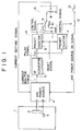
- Fig. 1 shows a block diagram of a control circuit in the first embodiment according to the present invention.
- Fig. 1 only the matters necessary for the explanation of the present invention are shown and others not necessary in view of the explanation are omitted even when they are actually necessary as a control device in the vacuum arc vapor deposition device.
- a cathode comprising an evaporation material (target) 2 and an anode 3 are disposed in a vacuum chamber 1, to which an electric power is supplied from an arc power source 4, to generate arc discharge and vaporize the target, to form a film on a substrate.
- an arc discharge current is taken out as a current monitor signal that can be monitored (a voltage signal in proportion with the current in this embodiment).
- the current monitor signal is intaken into a control device and converted into a pulse signal by a V/F converter 5. Since the number of pulses per unit time of the pulse signal is in proportion with the arc discharge current value, as the number of pulses is accumulated, the accumulated value is in proportion with the accumulated value of the arc discharge current with time. Accordingly, if the pulse accumulated value is multiplied with an appropriate constant, it can be converted into a time-accumulated value of the arc discharge current.
- two preset counters 6, 7 are used for the accumulation of the number of pulses.
- Each of the counters 6, 7 can be inputted with a reset signal for the counted value, and when the consumed part of the cathode (target) is consumed and replaced with new one, it is possible to reset the accumulated pulse value, that is, the time-accumulated value of the arc discharge current to zero.
- a setting value to the first preset counter 6 is determined as a value corresponding to the accumulated arc current value at which the target consumption is advanced and the evaporation amount is reduced, for example, by 10% of the initial stage.
- the first preset counter 6 When the accumulated value in the first preset counter 6 reaches the setting value, the first preset counter 6 generates a control signal to switch the voltage supplied to a current setting variable resistor 8 for setting the arc current from a 10 V power source 10 to an 11 V power source 11 by a switch 9. That is, the arc power source 4 controls its current output while receiving a voltage signal (current setting signal) from the control device, and the voltage signal is controlled by the operators' manipulation to the current setting variable resistor 8.
- the current setting signal can be increased by 10% without changing the setting of the current setting variable resistor 8. Accordingly, since the arc discharge current value is increased and the reduction of the target evaporation amount can be corrected, the evaporation amount can be controlled substantially constant.
- the second preset counter 7 functions in another way. That is, a value corresponding to the life of the target is set to the second preset counter as a setting value. When the accumulated value in the second preset counter 7 reaches the setting value by which the life of the target is detected, the second preset counter 7 generates a control signal to turn the switch 12 to OFF. Accordingly, although the power source switch 13 is kept ON as it is, ON signal sent from the control device to the arc power source 4 is automatically disconnected to interrupt the use of the target beyond its life. Accordingly, an accident caused by excess use of the target can be prevented.
- change of the evaporation property due to the consumption of the target can be corrected automatically and, if the target is consumed to its full life, it is also possible to automatically interrupt the arc discharge.
- the accumulating means 14 is constituted with the V/F converter 5 and the first preset counter 6, while the correcting means 15 is constituted with the variable resistor 8, the switch 9 and the power sources 10, 11.
- the embodiment described above shows a fundamental constitution applicable to such a device that the vapor deposition operation is conducted manually.
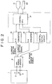
- a device in which the vapor deposition operation itself is completely automated by utilizing a computer or the like, since the present invention can be realized on a computer algorithm, application to a higher level is possible and the effect is improved.
- a current monitor signal from an arc power source 4 is read as information digitalized by an A/D converter 16 into a controlling CPU 17, while a current setting signal and an arc power source ON signal are, respectively, sent from a controlling CPU 17 by way of a D/A converter 18 and a control output circuit 10 to an arc power source 4 respectively.
- a change with time of film-forming conditions such as an arc current during one cycle are previously inputted, typically, from a key board 20 or the like as a program and vapor deposition operation of repeatingly operating the same is conducted.
- 21 denotes a CRT.
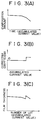
- the arc current value can be corrected by the accumulated value of the arc discharge current by using the data for the correcting amount as shown in Fig. 3(B). Accordingly, scattering of the film thickness between each of the processing lots can be reduced to such an extent as shown in Fig. 3(C) and processing with less scattering as compared with the existent case shown in Fig. 3(D) is possible.
- the accumulated arc current value corresponding to the target's life is previously determined and processing is interrupted at a stage in which the target reaches its life as shown already in the first embodiment, it can provide an effect of preventing the trouble of the device. Further, it is also preferred in view of improving the working efficiency of the device to issue an alarm at a stage where it reaches an accumulated value corresponding to, for example, 80% and 90% of the target life.
- a magnetic field is sometimes formed to the evaporation surface of a target with an aim of improving the utilization efficiency of the target, and the optimum strength or the shape of the magnetic field is generally changed depending on the state of consumption of the target. For instance, in a case of using magnet coils disposed at the back of the target as a means for forming the magnetic field the distance between the retracted evaporation surface and the coil is shortened, if the target is consumed, to excessively increase the magnetic field intensity on the evaporation surface as compared with that in the initial stage.
- the magnetic field on the target evaporation surface can be kept properly in such a case by recognizing the state of consumption by the accumulated value of the arc current and reducing the exciting current for the coils. Further, in a case where the optimum shape of the magnetic field changes due to the consumption of the target, a plurality of magnet coils can be disposed to the back of the target and exciting coil can be switched depending on the accumulated arc current value.
- the monitor signal of the arc current is processed to calculate the accumulated value of the arc current, but the invention is not restricted only thereto. For instance, it is also possible to determine a value corresponding to the accumulated arc current value by using the setting value for the arc current and conduct the same control, although it may be somewhat poor in view of the accuracy. Further, it is essentially in the scope of the present invention to accumulate the electric power supplied to the vacuum arc evaporation source, which is used in place of the accumulated current value, by utilizing the property of the vacuum arc discharge that the arc discharge voltage is substantially constant.
- the present invention comprises an accumulating means for accumulating with time an arc discharge current value of a vacuum arc evaporation source, and an correcting means for correcting the arc discharge current so that the evaporation amount from the vacuum arc evaporation source is substantially constant in accordance with the increase of the accumulated current value accumulated by the accumulating means, the evaporation property due to the consumption of the vacuum arc evaporation source can be corrected automatically and reproducibility between each of processing lots can be obtained automatically without operators' aid.
- a vacuum arc vapor deposition device comprising an accumulation means for accumulating with time an electric power supplied to a vacuum arc evaporation source and an correcting means for correcting an arc current value so that an evaporation amount from the vacuum arc evaporation source is substantially constant in accordance with the increase of the electric power accumulated by the accumulating means.
- the evaporation property due the consumption of the vacuum arc evaporation source can be corrected automatically and reproducibility between each of the processing lots can be obtained automatically without operators' aid.
Landscapes
- Chemical & Material Sciences (AREA)
- Engineering & Computer Science (AREA)
- Organic Chemistry (AREA)
- Materials Engineering (AREA)
- Mechanical Engineering (AREA)
- Metallurgy (AREA)
- Chemical Kinetics & Catalysis (AREA)
- Physics & Mathematics (AREA)
- Plasma & Fusion (AREA)
- Analytical Chemistry (AREA)
- Physical Vapour Deposition (AREA)
- Discharge Heating (AREA)
- Control Of Voltage And Current In General (AREA)
Applications Claiming Priority (2)
| Application Number | Priority Date | Filing Date | Title |
|---|---|---|---|
| JP77952/91 | 1991-04-10 | ||
| JP3077952A JP2758999B2 (ja) | 1991-04-10 | 1991-04-10 | 真空アーク蒸着装置 |
Publications (2)
| Publication Number | Publication Date |
|---|---|
| EP0508429A1 true EP0508429A1 (de) | 1992-10-14 |
| EP0508429B1 EP0508429B1 (de) | 1996-01-03 |
Family
ID=13648351
Family Applications (1)
| Application Number | Title | Priority Date | Filing Date |
|---|---|---|---|
| EP92106175A Expired - Lifetime EP0508429B1 (de) | 1991-04-10 | 1992-04-09 | Vorrichtung zum Vakuumbeschichten mittels Bogenentladung |
Country Status (4)
| Country | Link |
|---|---|
| US (1) | US5221349A (de) |
| EP (1) | EP0508429B1 (de) |
| JP (1) | JP2758999B2 (de) |
| DE (1) | DE69207251T2 (de) |
Cited By (2)
| Publication number | Priority date | Publication date | Assignee | Title |
|---|---|---|---|---|
| CN113093848A (zh) * | 2021-03-29 | 2021-07-09 | 中航电测仪器股份有限公司 | 一种基于电化学腐蚀方法的电阻应变片调阻电路及方法 |
| CN119332221A (zh) * | 2024-10-17 | 2025-01-21 | 京东方科技集团股份有限公司 | 修正装置、修正方法及蒸镀设备 |
Families Citing this family (16)
| Publication number | Priority date | Publication date | Assignee | Title |
|---|---|---|---|---|
| US5380415A (en) * | 1994-02-03 | 1995-01-10 | The United States Of America As Represented By The Administrator Of The National Aeronautics And Space Administration | Vacuum vapor deposition |
| CH688863A5 (de) * | 1994-06-24 | 1998-04-30 | Balzers Hochvakuum | Verfahren zum Beschichten mindestens eines Werkstueckes und Anlage hierfuer. |
| DE4440521C1 (de) * | 1994-11-12 | 1995-11-02 | Rowo Coating Ges Fuer Beschich | Vorrichtung zum Beschichten von Substraten mit einem Materialdampf im Unterdruck oder Vakuum |
| DE19539961C1 (de) * | 1995-01-14 | 1996-06-13 | Sintec Keramik Gmbh | Verfahren zum thermischen Verdampfen von elektrisch leitfähigen Materialien |
| DE19621855C2 (de) * | 1996-05-31 | 2003-03-27 | Univ Dresden Tech | Verfahren zur Herstellung von Metallisierungen auf Halbleiterkörpern unter Verwendung eines gepulsten Vakuumbogenverdampfers |
| US5932078A (en) * | 1997-08-30 | 1999-08-03 | United Technologies Corporation | Cathodic arc vapor deposition apparatus |
| US6009829A (en) * | 1997-08-30 | 2000-01-04 | United Technologies Corporation | Apparatus for driving the arc in a cathodic arc coater |
| US5972185A (en) * | 1997-08-30 | 1999-10-26 | United Technologies Corporation | Cathodic arc vapor deposition apparatus (annular cathode) |
| US6036828A (en) * | 1997-08-30 | 2000-03-14 | United Technologies Corporation | Apparatus for steering the arc in a cathodic arc coater |
| US6248408B1 (en) * | 1999-03-03 | 2001-06-19 | Vacuum Plating Technology Corporation | Method for simultaneously curing powder underlayer coating and PVD deposition of thin film layer |
| JP4679004B2 (ja) * | 2000-09-26 | 2011-04-27 | 新明和工業株式会社 | アーク蒸発源装置、その駆動方法、及びイオンプレーティング装置 |
| US9072169B1 (en) * | 2010-07-13 | 2015-06-30 | Cascodium Inc. | Pulse generator and systems and methods for using same |
| JP5644676B2 (ja) * | 2011-05-26 | 2014-12-24 | 三菱マテリアル株式会社 | アークイオンプレーティング装置および成膜方法 |
| JP5644675B2 (ja) * | 2011-05-26 | 2014-12-24 | 三菱マテリアル株式会社 | アークイオンプレーティング装置および成膜方法 |
| DE102012102007A1 (de) * | 2012-03-09 | 2013-09-12 | Infineon Technologies Ag | Leistungsversorgungsvorrichtung zum Liefern einer Spannung aus einem elektromagnetischen Feld |
| JPWO2024209533A1 (de) * | 2023-04-04 | 2024-10-10 |
Citations (4)
| Publication number | Priority date | Publication date | Assignee | Title |
|---|---|---|---|---|
| DD220618A1 (de) * | 1984-01-09 | 1985-04-03 | Mikroelektronik Zt Forsch Tech | Schaltungsanordnung zur targetverschleissbestimmung in sputteranlagen |
| US4512867A (en) * | 1981-11-24 | 1985-04-23 | Andreev Anatoly A | Method and apparatus for controlling plasma generation in vapor deposition |
| US4662312A (en) * | 1984-12-28 | 1987-05-05 | Nissin Electric Co., Ltd. | Apparatus for ion and vapor deposition |
| WO1989001699A1 (en) * | 1987-08-18 | 1989-02-23 | Regents Of The University Of Minnesota | Steered arc coating with thick targets |
Family Cites Families (3)
| Publication number | Priority date | Publication date | Assignee | Title |
|---|---|---|---|---|
| DE220618C (de) | 1909-06-22 | 1910-04-05 | ||
| DE3524981A1 (de) * | 1985-07-12 | 1987-01-22 | Siemens Ag | Anordnung mit einem saettigbaren carry-save-addierer |
| JPH0699799B2 (ja) * | 1988-03-18 | 1994-12-07 | 株式会社神戸製鋼所 | 真空蒸着方法 |
-
1991
- 1991-04-10 JP JP3077952A patent/JP2758999B2/ja not_active Expired - Lifetime
-
1992
- 1992-04-09 DE DE69207251T patent/DE69207251T2/de not_active Expired - Lifetime
- 1992-04-09 EP EP92106175A patent/EP0508429B1/de not_active Expired - Lifetime
- 1992-04-10 US US07/866,428 patent/US5221349A/en not_active Expired - Lifetime
Patent Citations (4)
| Publication number | Priority date | Publication date | Assignee | Title |
|---|---|---|---|---|
| US4512867A (en) * | 1981-11-24 | 1985-04-23 | Andreev Anatoly A | Method and apparatus for controlling plasma generation in vapor deposition |
| DD220618A1 (de) * | 1984-01-09 | 1985-04-03 | Mikroelektronik Zt Forsch Tech | Schaltungsanordnung zur targetverschleissbestimmung in sputteranlagen |
| US4662312A (en) * | 1984-12-28 | 1987-05-05 | Nissin Electric Co., Ltd. | Apparatus for ion and vapor deposition |
| WO1989001699A1 (en) * | 1987-08-18 | 1989-02-23 | Regents Of The University Of Minnesota | Steered arc coating with thick targets |
Non-Patent Citations (1)
| Title |
|---|
| PATENT ABSTRACTS OF JAPAN vol. 13, no. 575 (C-667)19 December 1989 & JP-A-1 240 645 ( KOBE STEEL LTD ) 26 September 1989 * |
Cited By (2)
| Publication number | Priority date | Publication date | Assignee | Title |
|---|---|---|---|---|
| CN113093848A (zh) * | 2021-03-29 | 2021-07-09 | 中航电测仪器股份有限公司 | 一种基于电化学腐蚀方法的电阻应变片调阻电路及方法 |
| CN119332221A (zh) * | 2024-10-17 | 2025-01-21 | 京东方科技集团股份有限公司 | 修正装置、修正方法及蒸镀设备 |
Also Published As
| Publication number | Publication date |
|---|---|
| US5221349A (en) | 1993-06-22 |
| DE69207251T2 (de) | 1996-05-30 |
| JP2758999B2 (ja) | 1998-05-28 |
| EP0508429B1 (de) | 1996-01-03 |
| DE69207251D1 (de) | 1996-02-15 |
| JPH04311560A (ja) | 1992-11-04 |
Similar Documents
| Publication | Publication Date | Title |
|---|---|---|
| EP0508429B1 (de) | Vorrichtung zum Vakuumbeschichten mittels Bogenentladung | |
| EP1970466B1 (de) | Verfahren und Steuersystem zum Aufbringen einer Schicht | |
| EP2013373B1 (de) | Verfahren und system zur aufbereitung eines aufdampfungsziels | |
| US6007879A (en) | Adjustable energy quantum thin film plasma processing system | |
| Belkind et al. | Using pulsed direct current power for reactive sputtering of Al 2 O 3 | |
| JPS6215633B2 (de) | ||
| US6416635B1 (en) | Method and apparatus for sputter coating with variable target to substrate spacing | |
| EP2036113B1 (de) | Verfahren zur regelung eines reaktiven hochleistungs-puls-magnetronsputterprozesses und vorrichtung hierzu | |
| KR100302000B1 (ko) | 스퍼터링용 전원 장치 및 이 장치를 이용한 스퍼터링 장치 | |
| JP4101554B2 (ja) | スパッタ装置及び方法 | |
| Schneider et al. | Reactive pulsed dc magnetron sputtering and control | |
| EP0710429A1 (de) | Verfahren zur anpassung des generators bei bipolaren niederdruck-glimmprozessen | |
| US4021636A (en) | Beam current control device for a technical corpuscular beam apparatus | |
| US6402904B1 (en) | System and method for performing sputter deposition using independent ion and electron sources and a target biased with an a-symmetric bi-polar DC pulse signal | |
| CN111519160B (zh) | 半导体沉积工艺补偿方法、补偿装置及半导体沉积设备 | |
| EP2794952B1 (de) | Niedertemperatur-lichtbogenionen-plattierbeschichtung | |
| JPH05202471A (ja) | マグネトロンスパッタリング装置 | |
| Tsuda et al. | Effects of phase regulation on ion energy distribution in RF bias sputtering | |
| WO1999004409A1 (en) | Power control apparatus for an ion source having an indirectly heated cathode | |
| Konstantinidis | High Power Impulse Magnetron Sputtering for the growth of functional metal oxide thin films | |
| Bandorf | Optical Emission Spectroscopy Monitoring and Active Control of Metallic and Reactive HIPIMS Processes | |
| JPS60197875A (ja) | スパツタ装置用自動成膜制御装置 | |
| CN113046701A (zh) | 成膜装置 | |
| Schneider et al. | Magnetron Sputtering and | |
| JPH06340972A (ja) | マグネトロンスパッタ装置およびマグネトロンスパッタ方法 |
Legal Events
| Date | Code | Title | Description |
|---|---|---|---|
| PUAI | Public reference made under article 153(3) epc to a published international application that has entered the european phase |
Free format text: ORIGINAL CODE: 0009012 |
|
| 17P | Request for examination filed |
Effective date: 19920409 |
|
| AK | Designated contracting states |
Kind code of ref document: A1 Designated state(s): DE FR GB |
|
| 17Q | First examination report despatched |
Effective date: 19950120 |
|
| GRAA | (expected) grant |
Free format text: ORIGINAL CODE: 0009210 |
|
| AK | Designated contracting states |
Kind code of ref document: B1 Designated state(s): DE FR GB |
|
| ET | Fr: translation filed | ||
| REF | Corresponds to: |
Ref document number: 69207251 Country of ref document: DE Date of ref document: 19960215 |
|
| PLBE | No opposition filed within time limit |
Free format text: ORIGINAL CODE: 0009261 |
|
| STAA | Information on the status of an ep patent application or granted ep patent |
Free format text: STATUS: NO OPPOSITION FILED WITHIN TIME LIMIT |
|
| 26N | No opposition filed | ||
| REG | Reference to a national code |
Ref country code: GB Ref legal event code: IF02 |
|
| PGFP | Annual fee paid to national office [announced via postgrant information from national office to epo] |
Ref country code: FR Payment date: 20030408 Year of fee payment: 12 |
|
| PGFP | Annual fee paid to national office [announced via postgrant information from national office to epo] |
Ref country code: GB Payment date: 20030409 Year of fee payment: 12 |
|
| PG25 | Lapsed in a contracting state [announced via postgrant information from national office to epo] |
Ref country code: GB Free format text: LAPSE BECAUSE OF NON-PAYMENT OF DUE FEES Effective date: 20040409 |
|
| GBPC | Gb: european patent ceased through non-payment of renewal fee |
Effective date: 20040409 |
|
| PG25 | Lapsed in a contracting state [announced via postgrant information from national office to epo] |
Ref country code: FR Free format text: LAPSE BECAUSE OF NON-PAYMENT OF DUE FEES Effective date: 20041231 |
|
| REG | Reference to a national code |
Ref country code: FR Ref legal event code: ST |
|
| PGFP | Annual fee paid to national office [announced via postgrant information from national office to epo] |
Ref country code: DE Payment date: 20110406 Year of fee payment: 20 |
|
| REG | Reference to a national code |
Ref country code: DE Ref legal event code: R071 Ref document number: 69207251 Country of ref document: DE |
|
| REG | Reference to a national code |
Ref country code: DE Ref legal event code: R071 Ref document number: 69207251 Country of ref document: DE |
|
| PG25 | Lapsed in a contracting state [announced via postgrant information from national office to epo] |
Ref country code: DE Free format text: LAPSE BECAUSE OF EXPIRATION OF PROTECTION Effective date: 20120410 |