EP0517005A2 - Tête magnétique à films minces à enroulements d'épaisseur variable - Google Patents
Tête magnétique à films minces à enroulements d'épaisseur variable Download PDFInfo
- Publication number
- EP0517005A2 EP0517005A2 EP92107969A EP92107969A EP0517005A2 EP 0517005 A2 EP0517005 A2 EP 0517005A2 EP 92107969 A EP92107969 A EP 92107969A EP 92107969 A EP92107969 A EP 92107969A EP 0517005 A2 EP0517005 A2 EP 0517005A2
- Authority
- EP
- European Patent Office
- Prior art keywords
- coil
- thin film
- leg
- head assembly
- film head
- Prior art date
- Legal status (The legal status is an assumption and is not a legal conclusion. Google has not performed a legal analysis and makes no representation as to the accuracy of the status listed.)
- Withdrawn
Links
Images


Classifications
-
- G—PHYSICS
- G11—INFORMATION STORAGE
- G11B—INFORMATION STORAGE BASED ON RELATIVE MOVEMENT BETWEEN RECORD CARRIER AND TRANSDUCER
- G11B5/00—Recording by magnetisation or demagnetisation of a record carrier; Reproducing by magnetic means; Record carriers therefor
- G11B5/127—Structure or manufacture of heads, e.g. inductive
- G11B5/31—Structure or manufacture of heads, e.g. inductive using thin films
- G11B5/3109—Details
- G11B5/313—Disposition of layers
-
- H—ELECTRICITY
- H05—ELECTRIC TECHNIQUES NOT OTHERWISE PROVIDED FOR
- H05K—PRINTED CIRCUITS; CASINGS OR CONSTRUCTIONAL DETAILS OF ELECTRIC APPARATUS; MANUFACTURE OF ASSEMBLAGES OF ELECTRICAL COMPONENTS
- H05K1/00—Printed circuits
- H05K1/16—Printed circuits incorporating printed electric components, e.g. printed resistors, capacitors or inductors
- H05K1/165—Printed circuits incorporating printed electric components, e.g. printed resistors, capacitors or inductors incorporating printed inductors
-
- H—ELECTRICITY
- H05—ELECTRIC TECHNIQUES NOT OTHERWISE PROVIDED FOR
- H05K—PRINTED CIRCUITS; CASINGS OR CONSTRUCTIONAL DETAILS OF ELECTRIC APPARATUS; MANUFACTURE OF ASSEMBLAGES OF ELECTRICAL COMPONENTS
- H05K2201/00—Indexing scheme relating to printed circuits covered by H05K1/00
- H05K2201/09—Shape and layout
- H05K2201/09209—Shape and layout details of conductors
- H05K2201/09654—Shape and layout details of conductors covering at least two types of conductors provided for in H05K2201/09218 - H05K2201/095
- H05K2201/09736—Varying thickness of a single conductor; Conductors in the same plane having different thicknesses
-
- H—ELECTRICITY
- H05—ELECTRIC TECHNIQUES NOT OTHERWISE PROVIDED FOR
- H05K—PRINTED CIRCUITS; CASINGS OR CONSTRUCTIONAL DETAILS OF ELECTRIC APPARATUS; MANUFACTURE OF ASSEMBLAGES OF ELECTRICAL COMPONENTS
- H05K2203/00—Indexing scheme relating to apparatus or processes for manufacturing printed circuits covered by H05K3/00
- H05K2203/05—Patterning and lithography; Masks; Details of resist
- H05K2203/0562—Details of resist
- H05K2203/0574—Stacked resist layers used for different processes
Definitions
- This invention relates to a method and means of making a thin film magnetic head and in particular to a magnetic head having conducting coils of varying thickness.
- thin film magnetic heads used with data storage apparatus typically comprise magnetic pole pieces and an electrically conductive coil structure disposed between the pole pieces.
- the tips of the pole pieces define a transducing gap for coaction with a magnetic medium, such as a magnetic disk that rotates close to the transducing gap of the head.
- the pole pieces interconnect at a back gap closure.
- a significant problem that is experienced with thin film magnetic heads is the relatively high coil resistance or transducer resistance.
- the power 1 2 R (where I is current and R is resistance)that is dissipated during the recording process is determined by the value of coil resistance
- the higher the resistance of the head coil structure the higher will be the power dissipation and the greater the extent of thermal expansion of the components of the recording head and the recording apparatus. Thermal expansion adversely affects the recording operation.
- the amount of thermal noise that is generated depends upon the level of coil resistance. This thermal noise is generated at the transducer level and will be amplified in the storage apparatus, resulting in an undesirable reduction of the signal-to-noise ratio of the recording process.
- Thin film heads typically have small geometries, when compared to prior art ferrite heads.
- coil pitch had to become smaller and smaller, which resulted in an increase in coil resistance.
- Presently known thin film heads are characterized by an average resistance of about 30 to 40 ohms for a 34 turn head, and 40 to 50 ohms for a 42 turn head, by way of example.
- ferrite heads have a resistance of 5 to 10 ohms for a 30 turn head. The difference in resistance occurs because the larger ferrite heads are able to use conductive wires or turns with a 25.4 to 50.8 microns diameter, while the cross-section of a thin film head turn is about 3-4 microns.
- transducer coils are made of electroplated copper having a resistivity in the range of about 1.8 to 2.2 ohms centimeter. Although silver has a lower resistivity of 1.59 ohms cm., the fabrication of silver coils is so complex that it would outweigh any advantage of a 3% reduction in resistance.
- An object of this invention is to provide a thin film head having a reduced coil resistance without degrading the performance of the magnetic head.
- Another object of this invention is to provide a thin film head that affords a relatively high signal output without any complex modification in the head structure or manufacturing process.
- a thin film magnetic head comprises pole piece layers P1 and P2 with one or more conductive coils deposited between the pole pieces.
- the portions of the coil structure under the operating magnetic portion of the transducer between the pole pieces are relatively thin, as is found with conventional thin film heads.
- the thickness of the coil portions outside of the magnetic yoke area are made substantially thicker to effectively reduce the overall electrical resistance of the transducer.
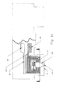
- a typical embodiment of a thin film head assembly comprises a ceramic substrate 10 preferably made of a material formed from a mixture of aluminum oxide (A1 2 0 3 ) and titanium carbide (TiC).
- the ceramic substrate 10 is polished to provide a smooth surface on which a layer of insulating aluminum oxide 12 is deposited by r.f. sputtering, for example.
- the insulating oxide layer 12 is lapped and polished to eliminate surface defects.
- an alloy formed from nickel and iron is deposited by r.f. sputtering over the insulating layer 12.
- the pattern of the pole piece P1 is formed by means of a mask using standard photolithographic processes.
- a thin film 14 of sputtered aluminum oxide is deposited over the entire surface of the P1 pole piece layer.
- the portion of the oxide film 14 in the area of the back gap of the transducer is removed by standard masking and etching to produce a transducing gap layer.
- the thin oxide film 14 which extends to the tips of pole pieces P1 and P2 provides the transducing gap at the transducing surface of the thin film head.
- the P1 pole piece and second pole piece P2 which is spaced above P1 and in virtual alignment with P1 provide a magnetic field between the pole pieces.
- the pole pieces are preferably made of a nickel-iron alloy.
- the insulation layer 16 serves as a smoothing layer that is fabricated after forming the pole piece P1 and provides a substantially planar surface for the deposition of a first coil structure 18 made of a layer of copper material.
- a second coil structure 22 is deposited over an insulating layer 20 that is formed over the first coil structure 18.
- the two coil structures 18 and 22 are tied at a connection 17.
- the electrical coils 18 and 22 which are fabricated between the pole pieces P1 and P2 conduct current within the magnetic field generated by the pole pieces.
- signals are directed to the coils 18 and 22 from an external data processing circuit to terminals 23 and 25.
- the data signals are transduced and converted to magnetic flux signals at the transducing gap 15 formed at the end of gap layer 14 and at the transducing surface of the thin film transducer or head 11.
- Organic insulation layers 16, 20 and 24 made of baked and hardened photoresist are interweaved between the P1 and P2 pole pieces and the coil structures 18 and 22.
- An insulating aluminum oxide overcoat layer 26 is r.f.sputtered over the entire thin film head structure to protect against deleterious ambient effects, such as humidity for example.
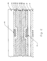
- the coil structures are each fabricated with two layers or legs.
- One leg of each coil structure is formed with a conventional thin layer and the second leg is formed to provide a much thicker layer of a portion of the coil structures. The thicker portion is located away from the P1 and P2 pole pieces and outside of the magnetic region between the pole pieces.
- the first leg 28 of the coil structure 38 is deposited by well known masking, sputtereing, plating and etching processes over the insulating gap layer 14 to form a step segment. Insulation layer 16 shown in Figs. 1 b and 2 is not depicted in Figs.
- the leg 28 is spaced from the P1 pole piece so that no portion of the leg 28 is disposed within the region of magnetic flux developed between P1 and P2.
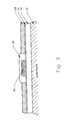
- the upper second layer or leg 32 of the first coil structure 38 is deposited over the first leg 28 and additionally over the portion of the insulation 30 formed above the P1 pole piece, as shown in Fig. 4.
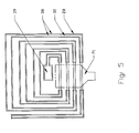
- Fig. 5 represents the first coil structure 38 with both layers of coils 28 and 32 connected at the interconnect pad 39.
- the thickness of the inner structure of upper second layer 32 of the first coil structure 38, disposed within the magnetic region of the transducer between the pole pieces, is relatively thin, in the range of about 2.5 to 4.0 microns, for example; and the thickness of the lower layer 28 of the first coil 38 outside the magnetic region, where the step segment 28 is provided, is made as thick as possible within manufacturing constraints. At present these manufacturing limitations allow the thickness of the layer 28 to be about the same as the thickness of the layer 32, which results in an overall thickness of the coil 38 of about twice the thickness of the layer 32, or about 5 to 8 microns thick.
- the second leg 32 of the first coil 38 is preferably made slightly narrower than the first leg 28 to facilitate coil-to-coil alignment.
- an organic insulation layer 20 is deposited over the second leg 32.
- the layer 20 provides leveling for facilitating the deposition of the first layer or leg 34 of the second coil structure 40, as shown in Fig. 6.
- the first leg 34 is substantially planar and is about the same thickness as the second leg 32 of the first coil 38.
- a second coil leg 36 is deposited on the leg 26 by a remask step, similar to the process step used for the first leg 28 of the first coil 38.
- the second leg 36 is thickened approximately to the level of the second pole P2.
- the leg 36 has a thickness substantially the same as the first leg 28 of the first coil 38.
- the coil structures 38 and 40 have configurations which are virtual mirror images of each other.
- An organic insulation layer 24 is next formed over the second leg 36 and the P2 pole piece is formed on the baked photoresist layer 24.
- a thick aluminum oxide insulation layer 26 is then deposited to serve as an overcoat and protective layer for the thin film magnetic head.
- the coils 38 and 40 are electrically connected to complete the signal circuit path.
- the other ends of the coils 38 and 40 are connected to pins or terminals which are coupled to external circuitry for passing signals through the head during recording and readout.
- the windings or turns of the coil structure 38 are made with a 5 micron pitch comprising 4 micron lines with a 1 micron spacing.
- the distance between the P1 pole piece and the bottom surface of the second leg or layer 32 of coil 38 was made to be about 2 to 5 microns.
- the insulation layers 16, 20, and 24 are made of organic material, i.e., a cured photoresist, which prevents the coils from electrical shorting to each other as well as to the pole pieces P1 and P2.
- the novel coil assembly incorporating coil structures having a plurality of coil layers, with one layer formed as a step adjacent to a thin coil layer to thicken the overall coil structure, a desirable reduction in coil resistance of a thin film head is realized.
- the step layer is made as thick as practically possible with present day manufacturing techniques, and is located out of the magnetic region defined by the opposing pole pieces.
- a single coil structure with a thin leg and a thick step leg may be produced to obtain a lowered coil resistance.
- the thicknesses of the coil layer may be varied to accommodate a specific configuration of a thin film head assembly.
- the step segment layer may be much thicker than the thin layer with the portion of the coil structure having the additional thickness outside of the magnetic yoke area thereby effectively decreasing coil resistance.
- a thin film head assembly includes a coil structure having a thin coil layer that extends within and beyond the magnetic yoke area delineated between opposing magnetic pole pieces, and an additional coil layer formed as a step segment adjacent to the thin layer.
- the additional layer is spaced away from the pole pieces and the magnetic yoke area and provides a thickened coil area which affords a significant reduction in coil resistance.
Landscapes
- Engineering & Computer Science (AREA)
- Manufacturing & Machinery (AREA)
- Magnetic Heads (AREA)
Applications Claiming Priority (2)
| Application Number | Priority Date | Filing Date | Title |
|---|---|---|---|
| US709333 | 1991-06-03 | ||
| US07/709,333 US5173826A (en) | 1991-06-03 | 1991-06-03 | Thin film head with coils of varying thickness |
Publications (2)
| Publication Number | Publication Date |
|---|---|
| EP0517005A2 true EP0517005A2 (fr) | 1992-12-09 |
| EP0517005A3 EP0517005A3 (en) | 1993-12-15 |
Family
ID=24849414
Family Applications (1)
| Application Number | Title | Priority Date | Filing Date |
|---|---|---|---|
| EP19920107969 Withdrawn EP0517005A3 (en) | 1991-06-03 | 1992-05-12 | Thin film head with coils of varying thickness |
Country Status (3)
| Country | Link |
|---|---|
| US (1) | US5173826A (fr) |
| EP (1) | EP0517005A3 (fr) |
| JP (1) | JPH05159234A (fr) |
Cited By (1)
| Publication number | Priority date | Publication date | Assignee | Title |
|---|---|---|---|---|
| EP1583077A3 (fr) * | 2004-03-30 | 2007-07-25 | Fujitsu Limited | Structure de tête magnétique avec couche d'isolation elargie |
Families Citing this family (22)
| Publication number | Priority date | Publication date | Assignee | Title |
|---|---|---|---|---|
| US5472736A (en) * | 1991-06-03 | 1995-12-05 | Read-Rite Corporation | Method of making a bi-level coil for a thin film magnetic transducer |
| US5831800A (en) * | 1992-05-05 | 1998-11-03 | Magnex Corporation | Miniature transformer for read/write transducer |
| JPH09180128A (ja) * | 1995-12-26 | 1997-07-11 | Read Rite S M I Kk | 薄膜磁気ヘッド |
| JPH09325403A (ja) * | 1996-06-05 | 1997-12-16 | Fuji Photo Film Co Ltd | 写真フイルム用磁気記録及び再生装置 |
| US6122149A (en) * | 1997-06-24 | 2000-09-19 | Seagate Technology, Inc. | Magnetic microactuator and inductive sensor having shaped pole configuration |
| US5875080A (en) * | 1997-09-05 | 1999-02-23 | International Business Machines Corporation | Write head with second coil above pole having coil density less electrically connected first coil below the pole |
| US6178070B1 (en) | 1999-02-11 | 2001-01-23 | Read-Rite Corporation | Magnetic write head and method for making same |
| US6400526B2 (en) | 1999-05-26 | 2002-06-04 | Read-Rite Corporation | Advanced writer for chip-on-load beam |
| CN1246829C (zh) * | 2000-06-20 | 2006-03-22 | 西加特技术有限责任公司 | 带有分层的写线圈的磁盘驱动器 |
| US6493183B1 (en) * | 2000-06-29 | 2002-12-10 | International Business Machines Corporation | Thermally-assisted magnetic recording system with head having resistive heater in write gap |
| JP3763526B2 (ja) * | 2002-04-04 | 2006-04-05 | Tdk株式会社 | マイクロデバイス及びその製造方法 |
| JP2004039090A (ja) * | 2002-07-03 | 2004-02-05 | Sony Corp | 磁気ヘッド装置並びにこれを用いた磁気テープドライブ装置及び磁気ディスクドライブ装置 |
| US6980395B2 (en) * | 2002-10-31 | 2005-12-27 | International Business Machines Corporation | Enhanced coplanar conductance structure for inductive heads |
| US7079353B2 (en) * | 2003-07-29 | 2006-07-18 | Hitachi Global Storage Technologies Netherlands B.V. | Magnetic head having a write coil structure with a reduced electrical resistance for reducing thermal protrusion |
| US20060034012A1 (en) * | 2003-08-29 | 2006-02-16 | Lam Terence T | Self-aligned coil process in magnetic recording heads |
| JP4945067B2 (ja) * | 2003-09-29 | 2012-06-06 | ヘッドウェイテクノロジーズ インコーポレイテッド | 薄膜磁気ヘッドおよびその製造方法並びにヘッドジンバルアセンブリおよびハードディスク装置 |
| JP2006164464A (ja) * | 2004-12-10 | 2006-06-22 | Alps Electric Co Ltd | 磁気ヘッド及びその製造方法 |
| JP2009205710A (ja) | 2008-02-26 | 2009-09-10 | Hitachi Global Storage Technologies Netherlands Bv | 垂直磁気記録ヘッドおよびその製造方法 |
| US8797684B1 (en) | 2011-12-20 | 2014-08-05 | Western Digital (Fremont), Llc | Magnetic writer configured for high data rate recording |
| US8786983B1 (en) | 2012-06-25 | 2014-07-22 | Western Digital (Fremont), Llc | Magnetic writer having a low aspect ratio two layer coil |
| US9245545B1 (en) | 2013-04-12 | 2016-01-26 | Wester Digital (Fremont), Llc | Short yoke length coils for magnetic heads in disk drives |
| US9196275B1 (en) | 2014-03-12 | 2015-11-24 | Western Digital Technologies, Inc. | Magnetic head separator fin material to prevent particulate contamination on slider |
Family Cites Families (13)
| Publication number | Priority date | Publication date | Assignee | Title |
|---|---|---|---|---|
| US3987488A (en) * | 1974-06-05 | 1976-10-19 | Matsushita Electric Industrial Co., Ltd. | Multi-tracks magnetic head with single turn winding structure |
| US4219854A (en) * | 1978-12-21 | 1980-08-26 | International Business Machines Corporation | Thin film magnetic head assembly |
| US4295173A (en) * | 1979-10-18 | 1981-10-13 | International Business Machines Corporation | Thin film inductive transducer |
| US4375657A (en) * | 1980-11-03 | 1983-03-01 | Brock George W | Magnetic head assembly |
| JPS5828838A (ja) * | 1981-08-14 | 1983-02-19 | Comput Basic Mach Technol Res Assoc | 薄膜磁気ヘッドの製造方法 |
| FR2559293B1 (fr) * | 1984-02-03 | 1988-09-09 | Commissariat Energie Atomique | Nouvelle tete magnetique d'ecriture et de lecture pour enregistrement magnetique et son procede de fabrication |
| US4752850A (en) * | 1984-06-06 | 1988-06-21 | Hitachi, Ltd. | Multi-track magnetic thin film heads |
| JPH07118057B2 (ja) * | 1984-08-06 | 1995-12-18 | 富士写真フイルム株式会社 | 薄膜磁気ヘッドの製造方法 |
| FR2575577B1 (fr) * | 1984-12-28 | 1989-07-07 | Bull Sa | Transducteur magnetique d'ecriture/lecture pour enregistrement perpendiculaire |
| US4713711A (en) * | 1985-05-08 | 1987-12-15 | International Business Machines | Thin film magnetic transducer having center tapped winding |
| JPS6271010A (ja) * | 1985-09-25 | 1987-04-01 | Hitachi Ltd | 磁気ヘツド |
| JPS6320079A (ja) * | 1986-07-11 | 1988-01-27 | ヤンマー農機株式会社 | 穀粒などの粒状体の感知センサ−装置 |
| NL9001147A (nl) * | 1990-05-17 | 1991-12-16 | Philips Nv | Dunnefilm magneetkop. |
-
1991
- 1991-06-03 US US07/709,333 patent/US5173826A/en not_active Expired - Lifetime
-
1992
- 1992-05-12 EP EP19920107969 patent/EP0517005A3/en not_active Withdrawn
- 1992-05-29 JP JP4138237A patent/JPH05159234A/ja active Pending
Cited By (1)
| Publication number | Priority date | Publication date | Assignee | Title |
|---|---|---|---|---|
| EP1583077A3 (fr) * | 2004-03-30 | 2007-07-25 | Fujitsu Limited | Structure de tête magnétique avec couche d'isolation elargie |
Also Published As
| Publication number | Publication date |
|---|---|
| JPH05159234A (ja) | 1993-06-25 |
| US5173826A (en) | 1992-12-22 |
| EP0517005A3 (en) | 1993-12-15 |
Similar Documents
| Publication | Publication Date | Title |
|---|---|---|
| US5173826A (en) | Thin film head with coils of varying thickness | |
| US6195232B1 (en) | Low-noise toroidal thin film head with solenoidal coil | |
| US5995342A (en) | Thin film heads having solenoid coils | |
| US6381095B1 (en) | High performance thin film magnetic write element having high Bsat poles and method for making same | |
| US6496330B1 (en) | Magnetic write head having a splitcoil structure | |
| US7522379B1 (en) | Write element with recessed pole and heat sink layer for ultra-high density writing | |
| US4295173A (en) | Thin film inductive transducer | |
| US7379269B1 (en) | Write element with reduced yoke length for ultra-high density writing | |
| US7238292B1 (en) | Method of fabricating a write element with a reduced yoke length | |
| EP0514600B1 (fr) | Dispositif transducteur/transformateur à film mince | |
| JP3345588B2 (ja) | 薄膜磁気ヘッド及びその製造方法 | |
| JP3149851B2 (ja) | 薄膜磁気ヘッド | |
| US5969911A (en) | Inductive/MR composite type thin-film magnetic head | |
| US5472736A (en) | Method of making a bi-level coil for a thin film magnetic transducer | |
| JPS59195311A (ja) | 垂直磁気ヘツド | |
| JPS61178710A (ja) | 薄膜磁気ヘツド及びその製造方法 | |
| KR100224648B1 (ko) | 두께가 변환된 코일이 설치된 박막헤드 | |
| JPH04356707A (ja) | 薄膜磁気ヘッド | |
| JP2551749B2 (ja) | 薄膜磁気ヘッドの製造方法 | |
| JP2722948B2 (ja) | 薄膜磁気ヘッド | |
| JPH01166309A (ja) | 薄膜磁気ヘッド | |
| JP2635670B2 (ja) | 薄膜磁気ヘッド | |
| JPH0721515A (ja) | 薄膜磁気ヘッド | |
| JPH06274827A (ja) | 垂直磁気記録用薄膜磁気ヘッド及びその製造方法 | |
| JPH10269525A (ja) | 薄膜磁気ヘッド及び磁気記録装置 |
Legal Events
| Date | Code | Title | Description |
|---|---|---|---|
| PUAI | Public reference made under article 153(3) epc to a published international application that has entered the european phase |
Free format text: ORIGINAL CODE: 0009012 |
|
| AK | Designated contracting states |
Kind code of ref document: A2 Designated state(s): DE FR GB NL |
|
| PUAL | Search report despatched |
Free format text: ORIGINAL CODE: 0009013 |
|
| AK | Designated contracting states |
Kind code of ref document: A3 Designated state(s): DE FR GB NL |
|
| 17P | Request for examination filed |
Effective date: 19940126 |
|
| 17Q | First examination report despatched |
Effective date: 19950905 |
|
| STAA | Information on the status of an ep patent application or granted ep patent |
Free format text: STATUS: THE APPLICATION IS DEEMED TO BE WITHDRAWN |
|
| 18D | Application deemed to be withdrawn |
Effective date: 19981201 |