EP0524766A2 - Dispositif d'affichage à cristaux liquides - Google Patents
Dispositif d'affichage à cristaux liquides Download PDFInfo
- Publication number
- EP0524766A2 EP0524766A2 EP92306495A EP92306495A EP0524766A2 EP 0524766 A2 EP0524766 A2 EP 0524766A2 EP 92306495 A EP92306495 A EP 92306495A EP 92306495 A EP92306495 A EP 92306495A EP 0524766 A2 EP0524766 A2 EP 0524766A2
- Authority
- EP
- European Patent Office
- Prior art keywords
- opposed
- pixels
- liquid crystal
- bus line
- pixel
- Prior art date
- Legal status (The legal status is an assumption and is not a legal conclusion. Google has not performed a legal analysis and makes no representation as to the accuracy of the status listed.)
- Granted
Links
Images



Classifications
-
- G—PHYSICS
- G02—OPTICS
- G02F—OPTICAL DEVICES OR ARRANGEMENTS FOR THE CONTROL OF LIGHT BY MODIFICATION OF THE OPTICAL PROPERTIES OF THE MEDIA OF THE ELEMENTS INVOLVED THEREIN; NON-LINEAR OPTICS; FREQUENCY-CHANGING OF LIGHT; OPTICAL LOGIC ELEMENTS; OPTICAL ANALOGUE/DIGITAL CONVERTERS
- G02F1/00—Devices or arrangements for the control of the intensity, colour, phase, polarisation or direction of light arriving from an independent light source, e.g. switching, gating or modulating; Non-linear optics
- G02F1/01—Devices or arrangements for the control of the intensity, colour, phase, polarisation or direction of light arriving from an independent light source, e.g. switching, gating or modulating; Non-linear optics for the control of the intensity, phase, polarisation or colour
- G02F1/13—Devices or arrangements for the control of the intensity, colour, phase, polarisation or direction of light arriving from an independent light source, e.g. switching, gating or modulating; Non-linear optics for the control of the intensity, phase, polarisation or colour based on liquid crystals, e.g. single liquid crystal display cells
- G02F1/133—Constructional arrangements; Operation of liquid crystal cells; Circuit arrangements
- G02F1/136—Liquid crystal cells structurally associated with a semi-conducting layer or substrate, e.g. cells forming part of an integrated circuit
-
- G—PHYSICS
- G09—EDUCATION; CRYPTOGRAPHY; DISPLAY; ADVERTISING; SEALS
- G09G—ARRANGEMENTS OR CIRCUITS FOR CONTROL OF INDICATING DEVICES USING STATIC MEANS TO PRESENT VARIABLE INFORMATION
- G09G3/00—Control arrangements or circuits, of interest only in connection with visual indicators other than cathode-ray tubes
- G09G3/20—Control arrangements or circuits, of interest only in connection with visual indicators other than cathode-ray tubes for presentation of an assembly of a number of characters, e.g. a page, by composing the assembly by combination of individual elements arranged in a matrix no fixed position being assigned to or needed to be assigned to the individual characters or partial characters
- G09G3/34—Control arrangements or circuits, of interest only in connection with visual indicators other than cathode-ray tubes for presentation of an assembly of a number of characters, e.g. a page, by composing the assembly by combination of individual elements arranged in a matrix no fixed position being assigned to or needed to be assigned to the individual characters or partial characters by control of light from an independent source
- G09G3/36—Control arrangements or circuits, of interest only in connection with visual indicators other than cathode-ray tubes for presentation of an assembly of a number of characters, e.g. a page, by composing the assembly by combination of individual elements arranged in a matrix no fixed position being assigned to or needed to be assigned to the individual characters or partial characters by control of light from an independent source using liquid crystals
- G09G3/3611—Control of matrices with row and column drivers
- G09G3/3648—Control of matrices with row and column drivers using an active matrix
-
- G—PHYSICS
- G09—EDUCATION; CRYPTOGRAPHY; DISPLAY; ADVERTISING; SEALS
- G09G—ARRANGEMENTS OR CIRCUITS FOR CONTROL OF INDICATING DEVICES USING STATIC MEANS TO PRESENT VARIABLE INFORMATION
- G09G2300/00—Aspects of the constitution of display devices
- G09G2300/08—Active matrix structure, i.e. with use of active elements, inclusive of non-linear two terminal elements, in the pixels together with light emitting or modulating elements
- G09G2300/0809—Several active elements per pixel in active matrix panels
-
- G—PHYSICS
- G09—EDUCATION; CRYPTOGRAPHY; DISPLAY; ADVERTISING; SEALS
- G09G—ARRANGEMENTS OR CIRCUITS FOR CONTROL OF INDICATING DEVICES USING STATIC MEANS TO PRESENT VARIABLE INFORMATION
- G09G2330/00—Aspects of power supply; Aspects of display protection and defect management
- G09G2330/08—Fault-tolerant or redundant circuits, or circuits in which repair of defects is prepared
Definitions
- the present invention relates to a liquid crystal display device and, more particularly, to an active matrix liquid crystal display device in a normally white mode.
- Characteristics of a liquid crystal display device are that it is thin and light, it can be driven at a low voltage, and display a colored image.
- This type of device has recently been employed as a display device for a personal computer, a wordprocessor, and the like.
- an active matrix liquid crystal display device including a switching element for each of pixels does not deteriorate in contrast or response even though the pixels are increased in number. It allows a half-tone display and is the most suitable for use in color television sets and office automation equipment.
- Fig. 10 shows a circuit equivalent to a conventional active matrix liquid crystal display device in which thin-film transistors (TFT) are used as switching elements.
- the liquid crystal display device includes two substrates (an array substrate and an opposed substrate) formed of a transparent insulation material such as glass, and a liquid crystal layer 8 interposed between these substrates. Pixels each having a TFT 3 and a transparent pixel electrode 4 are arranged in matrix on the array substrate.
- the transparent pixel electrode 4 is connected to the source of the TFT 3, and an address line 1 and a data line 2 are connected to the gate and drain thereof, respectively.
- An opposed electrode 7 is arranged on the opposed substrate so as to oppose to the transparent pixel electrodes 4.
- an address signal and a data signal are supplied to the address line 1 and data line 2 at predetermined timing, respectively, with the result that voltages corresponding to display can be selectively applied to the pixel electrodes 4.
- the orientation of the liquid crystal layer 8 ⁇ i.e. the light transmittance thereof ⁇ can be controlled by a difference in potential between the opposed electrode 7 and pixel electrodes 4, thereby allowing an arbitrary display.
- Liquid crystal in a twisted nematic mode is generally used for the liquid crystal layer 8, and a polarizing plate is formed on each of the outer faces of the substrates.
- Two display modes ⁇ a normally white mode and a normally black mode ⁇ can be achieved in accordance with the arrangement of the polarizing plate. More specifically, when no voltage is applied to the liquid crystal layer 8, the maximum light transmittance represents the normally white mode, whereas the minimum light transmittance indicates the normally black mode.
- the normally white mode is more frequently used.
- Defective pixels include a bright spot defective pixel which cause a bright spot defect on the screen of the liquid crystal display device when the screen is displayed black.
- the bright spot defective pixel degrades the display quality most.
- the the bright spot defect is caused in the liquid crystal display device in the normally white mode in a case where a voltage of a level which would cause the light transmittance of the liquid crystal layer to vary is not applied to the pixel electrode of the defect. Since there are many causes for this, the bright spot defect cannot be completely eliminated even by use of various types of redundant structures.
- the conventional active matrix liquid crystal display device in the normally white mode has a drawback in which its display quality is greatly degraded because of bright spot defective pixels.
- the present invention has been developed in consideration of the above situation and its object is to provide a liquid crystal display device capable of easily changing a bright spot defective pixel to a vanished spot defective pixel which is unnoticeable as a defect.
- the essence of the present invention is that one of bus lines to which predetermined voltages are applied can be connected to pixel electrodes, and a voltage drop in a liquid crystal layer due to a voltage drop in the pixel electrodes is compensated for, using the voltage applied to the bus line.
- the liquid crystal display device comprises: a matrix array substrate including pixel electrodes arranged in matrix, switching elements arranged for the respective pixel electrodes and driven in response to an address signal, and bus lines which are formed under the respective pixel electrodes, with insulation layers interposed therebetween and to which predetermined voltages are applied; a liquid crystal layer formed on the matrix array substrate; and an opposed substrate including an opposed electrode opposed to the pixel electrodes, with the liquid crystal layer interposed between the matrix array substrate and the opposed substrate, wherein a pixel electrode having represented a bright spot defect is short-circuited with one of the bus lines to which the predetermined voltages are applied.
- the bus lines include first and second bus lines to which preferably alternating current voltages, whose phases are opposite to each other, are applied. Assuming that the voltage applied to the first bus line is V1, the voltage applied to the second bus line is V2, the capacitance between the first bus line and the pixel electrode is C1, and the capacitance between the second bus line and the pixel electrode, C1 ⁇ V1 is almost equal to C2 ⁇ V2.
- the liquid crystal display device of the present invention if one of the first and second bus lines is short-circuited with the pixel electrode in the event that the voltage of the pixel electrode drops, the voltage drop can be compensated for. If the voltage applied to the bus line is set so that the compensated voltage of the pixel electrode is of a level which reduces the light transmittance of the liquid crystal layer, a bright spot defective pixel can be changed to a dark spot defective pixel which does not affect the display quality so much.
- a bright spot defective pixel which affects display quality the most adversely can be easily changed to a dark spot defective pixel which does not affect the quality so much.
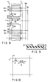
- Figs. 1 to 3 show a liquid crystal display device according to the first embodiment of the present invention.
- the liquid crystal display device comprises two substrates of a matrix array substrate 13 and an opposed substrate 14 formed of a transparent insulating material such as glass, and a liquid crystal layer 8 interposed between the substrates.
- a thin-film transistor (TFT) 3 and capacitors 5 and 6 are formed for one pixel of the liquid crystal display device.
- the gate of the TFT 3 is connected to an address line 1, the source/drain thereof is connected to a pixel electrode 4 through a connection wiring layer 12, and the other source/drain thereof is connected to a data line 2.
- the capacitors 5 and 6 are constituted of the pixel electrode 4 and bus lines 9 and 10 formed under an insulating film 11 made of, e.g., silicon oxide.
- the TFT 3 is a reverse stagger TFT whose gate electrode is constituted of part of the address line 1 formed under an active layer 15 with the insulating film 11 interposed between the address line 1 and the active layer 15.
- the active layer 15 is formed of amorphous silicon.
- a channel protection film 16 is formed on the active layer 15 to prevent the active layer 15 from being damaged during the manufacture of the TFT.
- the pixel electrode 4 is formed of transparent indium tin oxide (ITO).
- the capacitances C S1 and C S2 of the capacitors 5 and 6 are both 0.15 pF.
- the bus lines 9 and 10 are thin films of alloy of molybdenum and tantalum, and their widths are both 15 ⁇ m. As shown in Fig.
- alternating current bias voltages V B1 and V B2 whose central voltages V com are 5 V, amplitudes V01 and V02 are 4 V, and phases are shifted by 180° to each other, are applied to the bus lines 9 and 10, respectively.
- the cycles of the bias voltages V B1 and V B2 are both 30 Hz which corresponds to a value two times as large as a period 1/60 seconds necessary for selecting all the pixels or all the address lines 1 of the liquid crystal display device. If the amplitudes V01 and V02 of the bias voltages V B1 and V B2 are larger than that of a voltage at which the light transmittance of the liquid crystal layer starts to change, they need not be 4 V.
- the potential V com ′ of the opposed electrode 7 is set to 5 V to prevent a DC voltage from being applied to the liquid crystal layer 8.
- the bias voltages V B1 and V B2 have different phases which are shifted by 180° to each other, and satisfy the following equation (1).
- C S1 ⁇ V01 C S2 ⁇ V02
- a voltage ⁇ V S V corresponding to a difference between the potential of the opposed electrode 7 and pixel electrode potential V p can thus be applied to the liquid crystal layer 8 and, as in a conventional case, the light transmittance of the liquid crystal layer 8 can be controlled to achieve a desired display.
- a method of recovering a bright spot defective pixel of the liquid crystal display device having the above arrangement will be described. Assume that the connection wiring layer 12 is disconnected, and no voltage is applied to the pixel electrode 4, resulting in a bright spot defective pixel.
- a laser beam LB such as a YAG laser beam is emitted from the undersurface of the matrix array substrate 13 to partially damage the bus line 9 and insulating film 11, and the damaged bus line 9 and pixel electrode 4 are short-circuited by the melt of the bus line 9. Since, therefore, the pixel electrode potential V p is equalized with the bias voltage V B1 , a pulse voltage of 5 ⁇ 4 V is always applied to the pixel electrode 4. Further, since the potential V com ′ of the opposed electrode 7 is 5 V, a pulse voltage of ⁇ 4 V is applied to the liquid crystal layer 8. Since the light transmittance of the liquid crystal layer 8 is about 1% at ⁇ 4 V the bright spot defective pixel is changed to a dark spot defective pixel.
- the bias voltages V B1 and V B2 of the bus lines 9 and 10 may not conform to the equation (1) in a normal display operation because of the capacitance of the liquid crystal layer 8. If, however, the central voltage V com and the amplitudes V01 and V02 of the bias voltages V B1 and V B2 can be adjusted, they can satisfy the equation (1) in principle. Even though a few direct current components are applied to the dark spot defective pixel, no problems occur when the light transmittance is considerably low.
- a bright spot defective pixel having the most adverse influence on display quality can be changed to a dark spot defective pixel having less adverse influence thereon. Since the dark spot defective pixel is driven by alternating current voltage, the liquid crystal layer is not degraded by the change in the defective pixels.
- Fig. 5 is a plan view of one pixel of a liquid crystal display device according to the second embodiment of the present invention.
- the elements corresponding to those of the pixel of the first embodiment shown in Figs. 1 to 3 are denoted by the same reference numerals, and their descriptions are omitted.
- the liquid crystal display device of the second embodiment differs from that of the first embodiment in that the widths of the bus lines 9 and 10 are different from each other.
- the width of the bus line 9 is 10 ⁇ m and that of the bus line 10 is 20 ⁇ m.
- the capacitances C S1 and C S2 of the capacitors 5 and 6 are 0.1 pF and 0.2 pF, respectively.
- a pulse voltage whose amplitude is 5.0 ⁇ 5.0 V and cycle is 30 Hz, is applied to the bus line 9
- a pulse voltage whose amplitude is 5.0 ⁇ 2.5 V and cycle is 30 Hz
- the pulse voltages satisfy the equation (1), and no problems arise in the normal display operation of the second embodiment.
- a bright spot defective pixel of the second embodiment is recovered, as in the first embodiment.
- a YAG laser beam is emitted from the undersurface of the matrix array substrate to short-circuit the bus line 9 and pixel electrode 4 and apply a voltage of 5.0 ⁇ 5.0 V to the pixel electrode 4, with the result that the bright spot defective pixel is changed to a dark spot defective pixel.
- the capacitances C S1 and C S2 are set to different values in the second embodiment, the amplitude of the pulse voltage applied to the bus line 10 having a capacitor which is larger than that of the bus line 9, can be reduced. A pulse voltage necessary for changing the bright spot defective pixel to the dark spot defective pixel, is applied to the bus line 9.
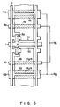
- Fig. 6 is a plan view of pixels of a liquid crystal display device according to the third embodiment of the present invention.
- the elements corresponding to those of the pixel of the first embodiment shown in Figs. 1 to 3 are denoted by the same reference numerals, and their descriptions are omitted.
- the liquid crystal display device of the third embodiment differs from that of the first embodiment in that a plurality of pixel electrodes are arranged for each pixel. More specifically, one pixel is divided into two sub-pixels, and a switching transistor 3a and a pixel electrode 4a are arranged for one of the subpixels and a switching transistor 3b and a pixel electrode 4b are arranged for the other sub-pixel.
- Bus lines 9a and 10a, and bus lines 9b and 10b are formed under the pixel electrodes 4a and 4b, respectively. The width of each of the bus lines 9a and 9b is 15 ⁇ m.
- the width of an overlap of the bus line 10a and pixel electrode 4a and that of an overlap of the bus line 10b and pixel electrode 4b are both 15 ⁇ m.
- the bus lines 10a and 10b are also used as those of sub-pixels of the adjacent pixels.
- Bias voltages each having an amplitude of 5.0 ⁇ 4 V and a cycle of 30 Hz are applied to the bus lines 9a and 9b, and 10a and 10b.
- the phases of the bias voltages applied to the bus lines 9a and 9b are opposite to these of the bias voltages applied to the bus lines 10a and 10b.
- the same signal is applied to the pixel electrodes 4a and 4b by the same process.
- the potential of the opposed electrode 7 is set to about 5 V.
- a bright spot defective pixel can be recovered if the bus line 9a or 9b and the pixel electrode of one of the bright spot defective sub-pixels are short-circuited by the laser beam to change it to a dark spot defective sub-pixel. Since most of bright spot defective pixels are randomly generated, both of two sub-pixels of one pixel seldom become defective at a time. In most cases, the bright spot defective pixel can be recovered only by changing one of the bright spot defective sub-pixels to a dark spot defective sub-pixel. Therefore, substantially the same display quality can be obtained as when a display operation is performed by normal pixels, even though the luminance of the pixel is reduced to half by the dark spot defective sub-pixel.
- Fig. 7 is a plan view of pixels of a liquid crystal display device according to the fourth embodiment of the present invention.
- the elements corresponding to those of the pixel of the first embodiment shown in Figs. 1 to 3 are denoted by the same reference numerals, and their descriptions are omitted.
- the fourth embodiment is a modification to the third embodiment shown in Fig. 6.
- one pixel is divided into two sub-pixels.
- the bus lines 10a and 10b are used in common to adjacent sub-pixels, and the capacitances of an overlap of the bus line 10a and the pixel electrode 4a and that of the bus line 10b and the pixel electrode 4b are set equal to those of an overlap of the bus line 9a and the pixel electrode 4a and that of the bus line 9b and the pixel electrode 4b.
- a difference may be caused between the capacitances C S1 and C S2 by mask displacement in the process for manufacturing a TFT array.
- the width or area of the bus lines 101 and 91 of a sub-pixel 41 is equal to that of the bus lines 102 and 92 of the adjacent sub-pixel 42. Furthermore, since the bus lines 101 and 102 are connected by a bypass 103, these bus lines are electrically connected to each other and supplied with the same signal, even if part of the bus lines is disconnected. If the bypass 103 is considerably narrow, a difference between the capacitances of the capacitors 51, 52, 61 and 62 due to the mask displacement, can be eliminated, and a predetermined signal can be supplied to the bus lines 101 and 102 even when they are disconnected.
- Fig. 8 is a circuit diagram schematically showing pixels of a liquid crystal display device according to the fifth embodiment of the present invention.
- the elements corresponding to those of the pixel of the third embodiment shown in Fig. 6 are denoted by the same reference numerals, and their descriptions are omitted.
- One cause of the bright spot defective pixel is a drop in pixel potential due to a defective TFT. It is difficult to distinguish the defective TFT from a normal TFT by their shapes, operations, etc. Generally, it is difficult to distinguish a bright spot defective pixel due to the defective TFT from that due to a defect in wiring connection. In the liquid crystal display device of the fifth embodiment, these two causes of the bright spot defective pixels can easily be distinguished from each other, and the defective pixels can be recovered in accordance with the causes.
- the liquid crystal display device of the fifth embodiment differs from that of the third embodiment in that each of the sub-pixels has two TFTs.
- the sub-pixel electrode 4a includes TFTs 3d and 3c.
- the TFT 3d is electrically connected to the pixel electrode 4a
- the TFT 3c is connected to the pixel electrode 4a via a connection wiring structure 20, but usually the TFT 3c is not electrically connected thereto.
- a wiring layer 21 connected to the TFT 3c and a wiring layer 23 connected to the pixel electrode 4a are formed opposite to a connection wiring layer 22 with the insulating film 11 interposed therebetween.
- the pixel sub-electrode 4b includes TFTs 3e and 3f.
- a bright spot defective pixel is recovered as follows. Assume that the bright spot defective pixel is generated by a voltage drop in the pixel electrode 4a.
- a wiring layer 24 connecting the TFT 3d and pixel electrode 4a is cut by the use of a laser to determine with the eye whether the voltage of the pixel electrode 4a has been dropped by a defect in the TFT 3d. If the bright spot defective pixel has been generated by the TFT 3d, a laser beam is emitted from the undersurface of the substrate 13 to connect the wiring layer 21 and connection wiring layer 22 and to connect the connection wiring layer 22 and wiring layer 23, thereby controlling the voltage of the pixel electrode 4a by the TFT 3c.
- one of two bus lines 9a and 9b are connected to the pixel electrode 4a using the laser to change the bright spot defective pixel to a dark spot defective pixel.
- the bright spot defective pixel due to not only a defect in connection of the wiring layers, but also a defect in characteristics of the TFTs, can easily be recovered.
- the pulse voltages whose phases are opposite to each other, have to be applied to the two bus lines 9a and 10a.
- no pulse voltage can be applied to the two bus lines or a predetermined direct current voltage can be applied thereto, with the result that power consumption of the device can be lowered.
- the present invention has the advantage that, if a bright spot defective pixel is generated by the short circuit of the capacitors through a pin hole of the insulating film of the capacitors, it is automatically changed to a dark spot defective pixel without using the laser beam.
- the present invention is not limited to the above embodiments.
- the potential of the opposed electrode is fixed.
- the present invention can be applied to a liquid crystal display device in which the potential of an opposed electrode is varied along scanning lines or frames.
- the pulse voltages whose phases are opposite to each other have only to be modulated so that the effect of two bus lines upon the potential of the pixel electrode is equal to that of one bus line. More specifically, the amplitudes and central voltages of the pulse voltages have only to be set to prevent a pulse bias of the bus lines from affecting the potential of the pixel electrode when a signal voltage is 0 V.
- the liquid crystal display devices according to the above embodiments are all black-and-white displays.
- the present invention can be applied to a color display using color filters.
- one pixel is constituted of unit pixels of red, blue and green in the color display, or of sub-pixels as in the third embodiments
- the unit pixels other than a defective unit pixel can be also changed to dark spot unit pixels. If only the defective unit pixel or sub-pixel is recovered, the balance of color is lost, and the display quality may be degraded. Therefore, normal unit pixels can be changed to dark spot unit pixels when the need arises to prevent the display quality from being degraded.
- the present invention can be applied to a liquid crystal display device using a three-terminal switching element or a two-terminal switching element other than a TFT.
Landscapes
- Physics & Mathematics (AREA)
- Engineering & Computer Science (AREA)
- General Physics & Mathematics (AREA)
- Chemical & Material Sciences (AREA)
- Crystallography & Structural Chemistry (AREA)
- Liquid Crystal (AREA)
- Computer Hardware Design (AREA)
- Nonlinear Science (AREA)
- Theoretical Computer Science (AREA)
- Optics & Photonics (AREA)
- Mathematical Physics (AREA)
- Microelectronics & Electronic Packaging (AREA)
- Liquid Crystal Display Device Control (AREA)
- Thin Film Transistor (AREA)
Applications Claiming Priority (2)
| Application Number | Priority Date | Filing Date | Title |
|---|---|---|---|
| JP181256/91 | 1991-07-22 | ||
| JP18125691A JP3150365B2 (ja) | 1991-07-22 | 1991-07-22 | 液晶表示装置 |
Publications (3)
| Publication Number | Publication Date |
|---|---|
| EP0524766A2 true EP0524766A2 (fr) | 1993-01-27 |
| EP0524766A3 EP0524766A3 (fr) | 1993-04-21 |
| EP0524766B1 EP0524766B1 (fr) | 1996-10-09 |
Family
ID=16097524
Family Applications (1)
| Application Number | Title | Priority Date | Filing Date |
|---|---|---|---|
| EP92306495A Expired - Lifetime EP0524766B1 (fr) | 1991-07-22 | 1992-07-15 | Dispositif d'affichage à cristaux liquides |
Country Status (5)
| Country | Link |
|---|---|
| US (1) | US5289174A (fr) |
| EP (1) | EP0524766B1 (fr) |
| JP (1) | JP3150365B2 (fr) |
| KR (1) | KR0128366B1 (fr) |
| DE (1) | DE69214372T2 (fr) |
Cited By (10)
| Publication number | Priority date | Publication date | Assignee | Title |
|---|---|---|---|---|
| US6636190B2 (en) * | 2000-10-12 | 2003-10-21 | Hitachi, Ltd. | Liquid crystal display having an improved lighting device |
| US9694749B2 (en) | 2001-01-23 | 2017-07-04 | Magna Electronics Inc. | Trailer hitching aid system for vehicle |
| US9694753B2 (en) | 2005-09-14 | 2017-07-04 | Magna Mirrors Of America, Inc. | Mirror reflective element sub-assembly for exterior rearview mirror of a vehicle |
| US9783114B2 (en) | 2000-03-02 | 2017-10-10 | Donnelly Corporation | Vehicular video mirror system |
| US9809171B2 (en) | 2000-03-02 | 2017-11-07 | Magna Electronics Inc. | Vision system for vehicle |
| US9809168B2 (en) | 2000-03-02 | 2017-11-07 | Magna Electronics Inc. | Driver assist system for vehicle |
| US9878670B2 (en) | 2002-09-20 | 2018-01-30 | Donnelly Corporation | Variable reflectance mirror reflective element for exterior mirror assembly |
| US10029616B2 (en) | 2002-09-20 | 2018-07-24 | Donnelly Corporation | Rearview mirror assembly for vehicle |
| US10144355B2 (en) | 1999-11-24 | 2018-12-04 | Donnelly Corporation | Interior rearview mirror system for vehicle |
| US10175477B2 (en) | 2008-03-31 | 2019-01-08 | Magna Mirrors Of America, Inc. | Display system for vehicle |
Families Citing this family (60)
| Publication number | Priority date | Publication date | Assignee | Title |
|---|---|---|---|---|
| JP2814161B2 (ja) * | 1992-04-28 | 1998-10-22 | 株式会社半導体エネルギー研究所 | アクティブマトリクス表示装置およびその駆動方法 |
| US6693681B1 (en) | 1992-04-28 | 2004-02-17 | Semiconductor Energy Laboratory Co., Ltd. | Electro-optical device and method of driving the same |
| US5910854A (en) | 1993-02-26 | 1999-06-08 | Donnelly Corporation | Electrochromic polymeric solid films, manufacturing electrochromic devices using such solid films, and processes for making such solid films and devices |
| US5668663A (en) | 1994-05-05 | 1997-09-16 | Donnelly Corporation | Electrochromic mirrors and devices |
| JPH08306926A (ja) * | 1995-05-07 | 1996-11-22 | Semiconductor Energy Lab Co Ltd | 液晶電気光学装置 |
| US6891563B2 (en) | 1996-05-22 | 2005-05-10 | Donnelly Corporation | Vehicular vision system |
| JP3688786B2 (ja) * | 1995-07-24 | 2005-08-31 | 富士通ディスプレイテクノロジーズ株式会社 | トランジスタマトリクス装置 |
| JP3338281B2 (ja) * | 1996-03-19 | 2002-10-28 | 株式会社東芝 | 液晶表示パネル |
| TW374852B (en) * | 1996-06-10 | 1999-11-21 | Toshiba Corp | Display device |
| JP3126661B2 (ja) | 1996-06-25 | 2001-01-22 | 株式会社半導体エネルギー研究所 | 液晶表示装置 |
| TW589504B (en) * | 1997-06-12 | 2004-06-01 | Sharp Kk | Liquid crystal display device |
| US8294975B2 (en) | 1997-08-25 | 2012-10-23 | Donnelly Corporation | Automotive rearview mirror assembly |
| US6172613B1 (en) | 1998-02-18 | 2001-01-09 | Donnelly Corporation | Rearview mirror assembly incorporating vehicle information display |
| US6326613B1 (en) | 1998-01-07 | 2001-12-04 | Donnelly Corporation | Vehicle interior mirror assembly adapted for containing a rain sensor |
| US6124886A (en) | 1997-08-25 | 2000-09-26 | Donnelly Corporation | Modular rearview mirror assembly |
| US8288711B2 (en) | 1998-01-07 | 2012-10-16 | Donnelly Corporation | Interior rearview mirror system with forwardly-viewing camera and a control |
| US6445287B1 (en) | 2000-02-28 | 2002-09-03 | Donnelly Corporation | Tire inflation assistance monitoring system |
| US6477464B2 (en) | 2000-03-09 | 2002-11-05 | Donnelly Corporation | Complete mirror-based global-positioning system (GPS) navigation solution |
| US6693517B2 (en) | 2000-04-21 | 2004-02-17 | Donnelly Corporation | Vehicle mirror assembly communicating wirelessly with vehicle accessories and occupants |
| JP3104687B2 (ja) * | 1998-08-28 | 2000-10-30 | 日本電気株式会社 | 液晶表示装置 |
| WO2001064481A2 (fr) | 2000-03-02 | 2001-09-07 | Donnelly Corporation | Systeme de miroir video integrant un module accessoire |
| JP3712637B2 (ja) | 2000-08-11 | 2005-11-02 | シャープ株式会社 | 液晶表示装置およびその欠陥修正方法 |
| JP4282219B2 (ja) * | 2000-11-28 | 2009-06-17 | 三洋電機株式会社 | 画素暗点化方法 |
| WO2002065203A1 (fr) * | 2001-02-15 | 2002-08-22 | Matsushita Electric Industrial Co., Ltd. | Affichage a cristaux liquides et procede de reparation de celui-ci |
| KR100796749B1 (ko) * | 2001-05-16 | 2008-01-22 | 삼성전자주식회사 | 액정 표시 장치용 박막 트랜지스터 어레이 기판 |
| TW594156B (en) * | 2002-01-04 | 2004-06-21 | Fujitsu Display Tech | Substrate for display device and display device equipped therewith |
| TW550531B (en) * | 2002-02-07 | 2003-09-01 | Chi Mei Optoelectronics Corp | Pixel driving device of liquid crystal display |
| US6918674B2 (en) | 2002-05-03 | 2005-07-19 | Donnelly Corporation | Vehicle rearview mirror system |
| WO2003105099A1 (fr) | 2002-06-06 | 2003-12-18 | Donnelly Corporation | Systeme de miroir de courtoisie interieur a boussole |
| US7329013B2 (en) | 2002-06-06 | 2008-02-12 | Donnelly Corporation | Interior rearview mirror system with compass |
| JP4050100B2 (ja) * | 2002-06-19 | 2008-02-20 | シャープ株式会社 | アクティブマトリクス基板および表示装置 |
| TW559756B (en) * | 2002-08-26 | 2003-11-01 | Chi Mei Optoelectronics Corp | Defective pixel remedy device and method of LCD panel |
| US7274501B2 (en) | 2002-09-20 | 2007-09-25 | Donnelly Corporation | Mirror reflective element assembly |
| US8537144B2 (en) * | 2002-11-29 | 2013-09-17 | Barco N.V. | Method and device for avoiding image misinterpretation due to defective pixels in a matrix display |
| US7446924B2 (en) | 2003-10-02 | 2008-11-04 | Donnelly Corporation | Mirror reflective element assembly including electronic component |
| US7308341B2 (en) | 2003-10-14 | 2007-12-11 | Donnelly Corporation | Vehicle communication system |
| JP4338511B2 (ja) | 2003-12-24 | 2009-10-07 | シャープ株式会社 | 液晶表示装置 |
| KR100680103B1 (ko) * | 2004-02-02 | 2007-02-28 | 샤프 가부시키가이샤 | 액정 표시 장치 |
| JP3891995B2 (ja) | 2004-04-26 | 2007-03-14 | シャープ株式会社 | 液晶表示装置 |
| JP4498043B2 (ja) | 2004-07-20 | 2010-07-07 | シャープ株式会社 | 液晶表示装置、液晶表示装置のリペア方法及び液晶表示装置の駆動方法 |
| KR20060035118A (ko) * | 2004-10-21 | 2006-04-26 | 김종하 | 엘피지 차량의 엘피엘아이 시스템용 가변식 엘피지압력조절장치 |
| KR100647774B1 (ko) * | 2004-11-04 | 2006-11-23 | 엘지.필립스 엘시디 주식회사 | 폴리 실리콘형 박막 트랜지스터 기판 및 제조 방법 |
| US7671932B2 (en) | 2005-03-18 | 2010-03-02 | Sharp Kabushiki Kaisha | Active matrix substrate and pixel defect correcting method therefor |
| EP1883855B1 (fr) | 2005-05-16 | 2011-07-20 | Donnelly Corporation | Ensemble de retroviseur de vehicule comportant des informations sur l'element reflecteur |
| US20070085805A1 (en) * | 2005-10-18 | 2007-04-19 | Seiko Epson Corporation | Electro-optical device and electronic apparatus |
| JP4678291B2 (ja) * | 2005-11-29 | 2011-04-27 | 三菱電機株式会社 | 表示装置及び表示装置の修復方法 |
| JP4927851B2 (ja) | 2006-09-12 | 2012-05-09 | シャープ株式会社 | マイクロレンズアレイ付き液晶表示パネル、その製造方法、および液晶表示装置 |
| WO2008038487A1 (fr) | 2006-09-28 | 2008-04-03 | Sharp Kabushiki Kaisha | Panneau d'affichage à cristaux liquides avec matrice de microlentilles, son procédé de fabrication et dispositif d'affichage à cristaux liquides |
| US20080117231A1 (en) | 2006-11-19 | 2008-05-22 | Tom Kimpe | Display assemblies and computer programs and methods for defect compensation |
| CN101568877B (zh) * | 2006-12-18 | 2011-05-11 | 夏普株式会社 | 液晶显示装置 |
| WO2008084589A1 (fr) | 2007-01-11 | 2008-07-17 | Sharp Kabushiki Kaisha | Panneau d'affichage à cristaux liquides et à réseau de microlentilles et dispositif d'affichage à cristaux liquides |
| KR101323250B1 (ko) * | 2007-02-28 | 2013-11-04 | 엘지디스플레이 주식회사 | 액정표시장치용 어레이 기판과 그 제조방법 |
| US20100118227A1 (en) * | 2007-03-28 | 2010-05-13 | Satoshi Shibata | Liquid cystal display panel with microlens array and method for manufacturing the same |
| KR101441387B1 (ko) * | 2007-12-27 | 2014-09-17 | 엘지디스플레이 주식회사 | 액정표시패널과 이의 제조방법 및 이를 이용한 리페어 방법 |
| TWI375828B (en) * | 2008-09-30 | 2012-11-01 | Au Optronics Corp | Pixel array, driving method for the same and display panel |
| CN102165363B (zh) * | 2008-09-30 | 2013-11-06 | 夏普株式会社 | 显示装置 |
| JP2014199899A (ja) | 2012-08-10 | 2014-10-23 | 株式会社半導体エネルギー研究所 | 半導体装置 |
| US9231002B2 (en) | 2013-05-03 | 2016-01-05 | Semiconductor Energy Laboratory Co., Ltd. | Display device and electronic device |
| GB2584618B (en) * | 2019-05-23 | 2022-03-23 | Jaguar Land Rover Ltd | Disabling navigation data for a vehicle |
| CN117321498A (zh) * | 2022-04-29 | 2023-12-29 | 京东方科技集团股份有限公司 | 显示基板及显示装置 |
Family Cites Families (3)
| Publication number | Priority date | Publication date | Assignee | Title |
|---|---|---|---|---|
| JPS59119390A (ja) * | 1982-12-25 | 1984-07-10 | 株式会社東芝 | 薄膜トランジスタ回路 |
| JPH0646351B2 (ja) * | 1984-11-27 | 1994-06-15 | セイコーエプソン株式会社 | アクティブマトリクス型液晶表示装置の駆動方法 |
| JPH0421823A (ja) * | 1990-05-16 | 1992-01-24 | Hosiden Corp | 液晶表示素子の点欠陥の黒欠陥化法及び液晶表示素子 |
-
1991
- 1991-07-22 JP JP18125691A patent/JP3150365B2/ja not_active Expired - Fee Related
-
1992
- 1992-07-14 US US07/913,069 patent/US5289174A/en not_active Expired - Lifetime
- 1992-07-15 DE DE69214372T patent/DE69214372T2/de not_active Expired - Fee Related
- 1992-07-15 EP EP92306495A patent/EP0524766B1/fr not_active Expired - Lifetime
- 1992-07-22 KR KR1019920013190A patent/KR0128366B1/ko not_active Expired - Fee Related
Cited By (28)
| Publication number | Priority date | Publication date | Assignee | Title |
|---|---|---|---|---|
| US10144355B2 (en) | 1999-11-24 | 2018-12-04 | Donnelly Corporation | Interior rearview mirror system for vehicle |
| US10239457B2 (en) | 2000-03-02 | 2019-03-26 | Magna Electronics Inc. | Vehicular vision system |
| US9783114B2 (en) | 2000-03-02 | 2017-10-10 | Donnelly Corporation | Vehicular video mirror system |
| US9809171B2 (en) | 2000-03-02 | 2017-11-07 | Magna Electronics Inc. | Vision system for vehicle |
| US9809168B2 (en) | 2000-03-02 | 2017-11-07 | Magna Electronics Inc. | Driver assist system for vehicle |
| US10179545B2 (en) | 2000-03-02 | 2019-01-15 | Magna Electronics Inc. | Park-aid system for vehicle |
| US10053013B2 (en) | 2000-03-02 | 2018-08-21 | Magna Electronics Inc. | Vision system for vehicle |
| US10131280B2 (en) | 2000-03-02 | 2018-11-20 | Donnelly Corporation | Vehicular video mirror system |
| US7683899B2 (en) | 2000-10-12 | 2010-03-23 | Hitachi, Ltd. | Liquid crystal display device having an improved lighting device |
| US6636190B2 (en) * | 2000-10-12 | 2003-10-21 | Hitachi, Ltd. | Liquid crystal display having an improved lighting device |
| US7138974B2 (en) | 2000-10-12 | 2006-11-21 | Hitachi, Ltd. | Liquid crystal display device having an improved lighting device |
| US9694749B2 (en) | 2001-01-23 | 2017-07-04 | Magna Electronics Inc. | Trailer hitching aid system for vehicle |
| US10272839B2 (en) | 2001-01-23 | 2019-04-30 | Magna Electronics Inc. | Rear seat occupant monitoring system for vehicle |
| US10538202B2 (en) | 2002-09-20 | 2020-01-21 | Donnelly Corporation | Method of manufacturing variable reflectance mirror reflective element for exterior mirror assembly |
| US10363875B2 (en) | 2002-09-20 | 2019-07-30 | Donnelly Corportion | Vehicular exterior electrically variable reflectance mirror reflective element assembly |
| US10661716B2 (en) | 2002-09-20 | 2020-05-26 | Donnelly Corporation | Vehicular exterior electrically variable reflectance mirror reflective element assembly |
| US10029616B2 (en) | 2002-09-20 | 2018-07-24 | Donnelly Corporation | Rearview mirror assembly for vehicle |
| US9878670B2 (en) | 2002-09-20 | 2018-01-30 | Donnelly Corporation | Variable reflectance mirror reflective element for exterior mirror assembly |
| US9758102B1 (en) | 2005-09-14 | 2017-09-12 | Magna Mirrors Of America, Inc. | Mirror reflective element sub-assembly for exterior rearview mirror of a vehicle |
| US10308186B2 (en) | 2005-09-14 | 2019-06-04 | Magna Mirrors Of America, Inc. | Vehicular exterior rearview mirror assembly with blind spot indicator |
| US10150417B2 (en) | 2005-09-14 | 2018-12-11 | Magna Mirrors Of America, Inc. | Mirror reflective element sub-assembly for exterior rearview mirror of a vehicle |
| US9694753B2 (en) | 2005-09-14 | 2017-07-04 | Magna Mirrors Of America, Inc. | Mirror reflective element sub-assembly for exterior rearview mirror of a vehicle |
| US10829053B2 (en) | 2005-09-14 | 2020-11-10 | Magna Mirrors Of America, Inc. | Vehicular exterior rearview mirror assembly with blind spot indicator |
| US11072288B2 (en) | 2005-09-14 | 2021-07-27 | Magna Mirrors Of America, Inc. | Vehicular exterior rearview mirror assembly with blind spot indicator element |
| US11285879B2 (en) | 2005-09-14 | 2022-03-29 | Magna Mirrors Of America, Inc. | Vehicular exterior rearview mirror assembly with blind spot indicator element |
| US11124121B2 (en) | 2005-11-01 | 2021-09-21 | Magna Electronics Inc. | Vehicular vision system |
| US11970113B2 (en) | 2005-11-01 | 2024-04-30 | Magna Electronics Inc. | Vehicular vision system |
| US10175477B2 (en) | 2008-03-31 | 2019-01-08 | Magna Mirrors Of America, Inc. | Display system for vehicle |
Also Published As
| Publication number | Publication date |
|---|---|
| DE69214372T2 (de) | 1997-03-27 |
| EP0524766B1 (fr) | 1996-10-09 |
| DE69214372D1 (de) | 1996-11-14 |
| JP3150365B2 (ja) | 2001-03-26 |
| KR0128366B1 (ko) | 1998-04-03 |
| KR930002864A (ko) | 1993-02-23 |
| JPH0527262A (ja) | 1993-02-05 |
| EP0524766A3 (fr) | 1993-04-21 |
| US5289174A (en) | 1994-02-22 |
Similar Documents
| Publication | Publication Date | Title |
|---|---|---|
| EP0524766B1 (fr) | Dispositif d'affichage à cristaux liquides | |
| JP3418653B2 (ja) | アクティブマトリクス型液晶表示装置 | |
| CN100582900C (zh) | 液晶显示器件 | |
| EP0456338B1 (fr) | Dispositif d'affichage à matrice active et son procédé de préparation | |
| US5469025A (en) | Fault tolerant active matrix display device | |
| US20090174829A1 (en) | Liquid crystal display apparatus | |
| US7375773B2 (en) | Active matrix substrate and display device | |
| JPH09288260A (ja) | 液晶表示装置、およびその駆動方法 | |
| US6864871B1 (en) | Active-matrix liquid crystal display apparatus and method for driving the same and for manufacturing the same | |
| WO2007034596A1 (fr) | Substrat de matrice active, écran, téléviseur, procédé de fabrication d’un substrat de matrice active, et procédé de fabrication d’un écran | |
| JPH1172806A (ja) | アクティブマトリクス型表示装置 | |
| JP2004212951A (ja) | 液晶表示素子及びその製造方法 | |
| EP0482737B1 (fr) | Dispositif d'affichage à matrice active | |
| US7817125B2 (en) | Display device | |
| CN100399171C (zh) | 液晶显示器 | |
| US20040223006A1 (en) | Liquid crystal display device | |
| JP3332106B2 (ja) | 液晶表示装置 | |
| JPH0434412A (ja) | アクティブマトリックス型液晶表示素子及びその駆動方法 | |
| JPH04346318A (ja) | 液晶表示装置 | |
| JPH05119742A (ja) | 液晶パネル駆動方法 | |
| JP3179319B2 (ja) | マトリクス型表示装置の欠陥検出方法 | |
| JPH0414091A (ja) | アクティブマトリクス型表示装置及びその制御方法 | |
| KR100917003B1 (ko) | 액정표시장치 | |
| JPH01277820A (ja) | 薄膜トランジスタ | |
| JP2000002885A (ja) | アクティブマトリクス型液晶表示装置 |
Legal Events
| Date | Code | Title | Description |
|---|---|---|---|
| PUAI | Public reference made under article 153(3) epc to a published international application that has entered the european phase |
Free format text: ORIGINAL CODE: 0009012 |
|
| 17P | Request for examination filed |
Effective date: 19920803 |
|
| AK | Designated contracting states |
Kind code of ref document: A2 Designated state(s): DE FR GB |
|
| PUAL | Search report despatched |
Free format text: ORIGINAL CODE: 0009013 |
|
| AK | Designated contracting states |
Kind code of ref document: A3 Designated state(s): DE FR GB |
|
| 17Q | First examination report despatched |
Effective date: 19950206 |
|
| GRAH | Despatch of communication of intention to grant a patent |
Free format text: ORIGINAL CODE: EPIDOS IGRA |
|
| GRAH | Despatch of communication of intention to grant a patent |
Free format text: ORIGINAL CODE: EPIDOS IGRA |
|
| GRAA | (expected) grant |
Free format text: ORIGINAL CODE: 0009210 |
|
| AK | Designated contracting states |
Kind code of ref document: B1 Designated state(s): DE |
|
| REF | Corresponds to: |
Ref document number: 69214372 Country of ref document: DE Date of ref document: 19961114 |
|
| EN | Fr: translation not filed | ||
| PLBE | No opposition filed within time limit |
Free format text: ORIGINAL CODE: 0009261 |
|
| STAA | Information on the status of an ep patent application or granted ep patent |
Free format text: STATUS: NO OPPOSITION FILED WITHIN TIME LIMIT |
|
| 26N | No opposition filed | ||
| PGFP | Annual fee paid to national office [announced via postgrant information from national office to epo] |
Ref country code: DE Payment date: 20060713 Year of fee payment: 15 |
|
| PG25 | Lapsed in a contracting state [announced via postgrant information from national office to epo] |
Ref country code: DE Free format text: LAPSE BECAUSE OF NON-PAYMENT OF DUE FEES Effective date: 20080201 |