EP0528311A2 - Elektrische Durchführungsstruktur und Herstellungsverfahren - Google Patents
Elektrische Durchführungsstruktur und Herstellungsverfahren Download PDFInfo
- Publication number
- EP0528311A2 EP0528311A2 EP92113566A EP92113566A EP0528311A2 EP 0528311 A2 EP0528311 A2 EP 0528311A2 EP 92113566 A EP92113566 A EP 92113566A EP 92113566 A EP92113566 A EP 92113566A EP 0528311 A2 EP0528311 A2 EP 0528311A2
- Authority
- EP
- European Patent Office
- Prior art keywords
- dielectric
- substrate
- electrical
- opening
- cell
- Prior art date
- Legal status (The legal status is an assumption and is not a legal conclusion. Google has not performed a legal analysis and makes no representation as to the accuracy of the status listed.)
- Granted
Links
Images


Classifications
-
- H—ELECTRICITY
- H10—SEMICONDUCTOR DEVICES; ELECTRIC SOLID-STATE DEVICES NOT OTHERWISE PROVIDED FOR
- H10F—INORGANIC SEMICONDUCTOR DEVICES SENSITIVE TO INFRARED RADIATION, LIGHT, ELECTROMAGNETIC RADIATION OF SHORTER WAVELENGTH OR CORPUSCULAR RADIATION
- H10F77/00—Constructional details of devices covered by this subclass
- H10F77/20—Electrodes
- H10F77/206—Electrodes for devices having potential barriers
- H10F77/211—Electrodes for devices having potential barriers for photovoltaic cells
-
- H—ELECTRICITY
- H05—ELECTRIC TECHNIQUES NOT OTHERWISE PROVIDED FOR
- H05K—PRINTED CIRCUITS; CASINGS OR CONSTRUCTIONAL DETAILS OF ELECTRIC APPARATUS; MANUFACTURE OF ASSEMBLAGES OF ELECTRICAL COMPONENTS
- H05K3/00—Apparatus or processes for manufacturing printed circuits
- H05K3/0011—Working of insulating substrates or insulating layers
- H05K3/0055—After-treatment, e.g. cleaning or desmearing of holes
-
- H—ELECTRICITY
- H05—ELECTRIC TECHNIQUES NOT OTHERWISE PROVIDED FOR
- H05K—PRINTED CIRCUITS; CASINGS OR CONSTRUCTIONAL DETAILS OF ELECTRIC APPARATUS; MANUFACTURE OF ASSEMBLAGES OF ELECTRICAL COMPONENTS
- H05K2201/00—Indexing scheme relating to printed circuits covered by H05K1/00
- H05K2201/01—Dielectrics
- H05K2201/0137—Materials
- H05K2201/0154—Polyimide
-
- H—ELECTRICITY
- H05—ELECTRIC TECHNIQUES NOT OTHERWISE PROVIDED FOR
- H05K—PRINTED CIRCUITS; CASINGS OR CONSTRUCTIONAL DETAILS OF ELECTRIC APPARATUS; MANUFACTURE OF ASSEMBLAGES OF ELECTRICAL COMPONENTS
- H05K2201/00—Indexing scheme relating to printed circuits covered by H05K1/00
- H05K2201/09—Shape and layout
- H05K2201/09209—Shape and layout details of conductors
- H05K2201/095—Conductive through-holes or vias
- H05K2201/09581—Applying an insulating coating on the walls of holes
-
- H—ELECTRICITY
- H05—ELECTRIC TECHNIQUES NOT OTHERWISE PROVIDED FOR
- H05K—PRINTED CIRCUITS; CASINGS OR CONSTRUCTIONAL DETAILS OF ELECTRIC APPARATUS; MANUFACTURE OF ASSEMBLAGES OF ELECTRICAL COMPONENTS
- H05K3/00—Apparatus or processes for manufacturing printed circuits
- H05K3/0011—Working of insulating substrates or insulating layers
- H05K3/0017—Etching of the substrate by chemical or physical means
- H05K3/0026—Etching of the substrate by chemical or physical means by laser ablation
- H05K3/0032—Etching of the substrate by chemical or physical means by laser ablation of organic insulating material
-
- Y—GENERAL TAGGING OF NEW TECHNOLOGICAL DEVELOPMENTS; GENERAL TAGGING OF CROSS-SECTIONAL TECHNOLOGIES SPANNING OVER SEVERAL SECTIONS OF THE IPC; TECHNICAL SUBJECTS COVERED BY FORMER USPC CROSS-REFERENCE ART COLLECTIONS [XRACs] AND DIGESTS
- Y02—TECHNOLOGIES OR APPLICATIONS FOR MITIGATION OR ADAPTATION AGAINST CLIMATE CHANGE
- Y02E—REDUCTION OF GREENHOUSE GAS [GHG] EMISSIONS, RELATED TO ENERGY GENERATION, TRANSMISSION OR DISTRIBUTION
- Y02E10/00—Energy generation through renewable energy sources
- Y02E10/50—Photovoltaic [PV] energy
-
- Y—GENERAL TAGGING OF NEW TECHNOLOGICAL DEVELOPMENTS; GENERAL TAGGING OF CROSS-SECTIONAL TECHNOLOGIES SPANNING OVER SEVERAL SECTIONS OF THE IPC; TECHNICAL SUBJECTS COVERED BY FORMER USPC CROSS-REFERENCE ART COLLECTIONS [XRACs] AND DIGESTS
- Y10—TECHNICAL SUBJECTS COVERED BY FORMER USPC
- Y10S—TECHNICAL SUBJECTS COVERED BY FORMER USPC CROSS-REFERENCE ART COLLECTIONS [XRACs] AND DIGESTS
- Y10S428/00—Stock material or miscellaneous articles
- Y10S428/901—Printed circuit
Definitions
- This invention relates to the structure and fabrication of electrical feedthroughs, and more particularly to a conductive via structure and fabrication method used to electrically connect the front face of a solar cell to its back face in a coplanar contact configuration.
- multilayer or 3-D integrated circuit chips can be stacked on top of each other, with circuitry on the upper face of each chip interconnected with circuitry on the other chips by means of conductive vias through the chips.
- Multilayer photonic devices also make use of electrical feedthroughs through the individual layers.
- a solar (photovoltaic) cell in which a voltage differential is developed across the opposite faces of the cell, but it is desired to electrically contact both faces with coplanar contacts made to the back face alone. While the present invention is primarily concerned with a coplanar contact solar cell, it is generally applicable to electrical feedthroughs for other applications also.
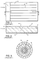
- FIGs. 1 and 2 A conventional solar cell 2 is illustrated in FIGs. 1 and 2.
- the cell is formed from a semiconductor material such as silicon, with its front face 4 oriented for illumination by the sun.
- An abrupt discontinuity in the conductivity type of the cell material is created through the addition of dopants.
- the portion of the semiconductor above junction 6 is doped n-type, while the portion below junction 6 is doped p-type.
- the semiconductor will absorb characteristic photon energies from the visible light spectrum to produce photo-generated electrical carriers, and thus induce a voltage differential between the front face 4 and rear face 8 of the cell.
- An electrical connection is made to the front face of the cell by means of conductive leads 10 that extend across the front face and are connected together by a conductive strip 12 along one edge of the cell.
- This configuration allows sunlight to enter the cell through the areas that are not shaded by the front face conductors; typically about 95% of the front face is exposed.
- Contact to the rear face 8 is made by means of a metallic sheet 14 which may cover that face.
- the voltage developed by the cell can be accessed by making separate electrical contacts to the terminal strip 12 and conductive sheet 14.
- both connections be made to only one side of the cell.
- the increased complexity of building a coplanar contact cell both contacts on only one side of the cell is more than offset by the reduced assembly cost of the coplanar configuration.
- an extension of the terminal strip 12 may be wrapped around the edge of the cell and brought to an area on the back face that is insulated from the conductive sheet 14 and the semiconductor material on that side of the cell.
- This type of connection which is referred to as a "wraparound" contact, is disclosed in numerous publications such as M. Gillanders et al., "High Efficiency Wraparound Contact Solar Cells", Proceedings of the 14th Photovoltaic Science Conference (PVSC) , 1980, pages 146-150; K. Matthei, "Optimization of Large Area Solar Cells for Low Cost Space Application", Proceedings of the 15th PVSC , 1981, pages 228-232; D.
- FIG. 3 shows a portion of the front face for a solar cell that has a radial and concentric circular network of conductor lines 16, rather than the rectangular grid lines 10 of FIGs. 1 and 2.
- the conductive lines 16 radiate outward from a terminal ring 18 to which they are all electrically connected.
- An opening or “via” 20 is centrally located within terminal ring 18, and extends down through the cell to the back face.
- the conductive material of terminal ring 18 extends through via 20 and coats its interior walls to establish an electrical connection between the front face conductor lines 16 and the back face of the cell.
- a similar via can be provided between the terminal strip 12 and the back face of the cell shown in FIGs. 1 and 2.
- Such "wrapthrough” vias are disclosed in several articles, such as D. Lillington et al., "Development of 8cm x 8cm Silicon Gridded Back Solar Cell for Space Station", Proceedings of the 19th PVSC , 1987, pages 489-493; D. Lillington et al., "Optimization of Silicon 8cm x 8cm Wrapthrough Space Station Cells for 'On Orbit' Operation", Proceedings of the 20th PVSC , 1988, pages 934-939; and A. Mason et al., “Development of 2.7 mil BSF and BSFR Silicon Wrapthrough Solar Cells", Proceedings of the 21st PVSC , 1990, pages 1378-1382.
- FIG. 4 An example of a prior "wrapthrough" via is shown in FIG. 4.
- An active solar cell region 22 is formed on a doped semiconductor substrate 24 that electrically functions as a conductor to bring the voltage developed on the underside of the active region to the cell's back face 26.
- a via opening 28 is established through the substrate, normally by laser scribing.
- a dielectric layer 30, typically SiO2 is deposited over the via walls and the adjacent front and back surfaces of the cell by low pressure chemical vapor deposition.
- a conductive metallic layer 32 is then deposited over the SiO2 layer 30, and extends beyond the dielectric on the front face of the cell to establish electrical contact with that portion of the active region.
- the conductive layer 32 is insulated from the substrate on its back face, but is exposed at that location so that it may be contacted coplanar with back face contact (not shown).
- the exposed substrate surface which contacts the SiO2 coating in the via opening be quite smooth, as illustrated on the left hand side of the via 28. If the substrate surface is rough it may not be completely covered by the SiO2 layer. In this event the conductive metal 32 can come near or into direct contact with the substrate, resulting in a significant power loss and perhaps even short-circuiting the device entirely.
- a problem with laser scribing via openings through semiconductors such as silicon and germanium is that the scribing operation produces an opening whose surface is quite rough.
- An aggressive etch is then typically employed to smooth the walls of the opening. Omitting the etch can result in the formation of pinholes or cracks in the SiO2 layer, resulting in the shunting of current into the substrate.
- Solar cells have recently been developed with GaAs active regions on a Ge substrate. While these materials offer a higher conversion efficiency than silicon, GaAs is attacked by the strong etchants used to smooth the via walls, and must be isolated from the etchant by a protective mask. Unfortunately, it is difficult to fully mask the GaAs active region, and damage often results from the etching process. In theory this problem can be overcome by reversing the fabrication process, and forming the via through the Ge substrate before the GaAs active region is grown. But the process of forming the via often results in damage to the upper Ge surface so that a good epitaxial growth of GaAs upon the substrate surface cannot be achieved.
- the degree to which cell performance is degraded by this type of limited shorting is a function of the shunt resistance value, the operating voltage and the cell area. Based upon modeled results for GaAs/Ge cells, minimum shunt resistances of 400 ohms and 6,000 ohms are required to hold losses to less than 0.5% for cells with areas of 16 cm2 and 1 cm2, respectively.
- the conventional via structure described above is not capable of reliably meeting this requirement.
- dielectrics such as SiO2 that are deposited by low pressure chemical vapor deposition have poor adhesion to Ge.
- the present invention seeks to provide a new via structure and fabrication method that substantially increases the via's shunt resistance and thus reduces power losses and eliminates the danger of shorting, eliminates the need for chemical etching to smooth the via surface in the substrate and thus allows the active region of a solar cell to be grown prior to forming the via, and exhibits good adhesion between the dielectric and both the substrate and the via metallization.
- a first opening is initially made through the substrate, the first opening is coated and substantially closed with a dielectric material, and a second opening is then formed through the dielectric.
- a coating of conductive material that extends between the opposed sides of the substrate is thereafter deposited over the dielectric, which insulates it from the substrate.
- the dielectric preferably comprises a material that is liquid in its uncured state, but is curable to a solid.
- the dielectric is first applied in its liquid state, and is thereafter cured. A partial cure may be performed prior to the formation of the opening through the dielectric, with the dielectric fully cured thereafter.
- a polyimide is preferred for the dielectric because of its superior adhesion to Ge and high temperature stability.
- the via opening may be formed with bevel profiles on each side interconnected by a narrower passageway.
- the dielectric thickness is substantially greater in the passageway than in the beveled areas removed from the passageway.
- the invention allows the opening through the dielectric to be made substantially smoother than the initial via opening through the substrate, and in the case of a GaAs/Ge solar cell permits the GaAs active region to be epitaxially grown upon the Ge base prior to forming the via.
- the new via structure eliminates the need for a chemical etch to smooth the surface of the initial via opening, unintended damage to the active region from etchant leakage is likewise eliminated.
- the new via structure also substantially increases the resistance of the via to current leakage, and thereby improves the cell's efficiency.
- the present invention takes a significant departure from the conventional approach to forming vias. Rather than simply forming a dielectric coating over a via opening to insulate the conductive layer from the substrate, it fully or partially encapsulates the via opening, closing it off. A new, narrower opening is then formed through the dielectric, and this provides the base for the conductive coating.
- the encapsulation approach allows for thicker dielectric layers that obviate the problems of rough via walls, and broadens the range of dielectric materials that may be used to include materials with better adhesion and insulating properties for the particular application.
- FIGs. 5a-5c The fabrication process for one embodiment is illustrated in FIGs. 5a-5c. A solar cell is shown, but the invention is also applicable to other types of electrical circuit packages in which a feedthrough is needed between opposed faces.
- a solar cell substrate 34 is shown with an active layer 36 grown on its upper (front) surface.
- a via opening 38 of a conventional type is formed through the substrate, either mechanically by grinding or drilling, or by a laser scribe technique in which the substrate stage is moved under a pulsed YAG laser to produce a via opening of the desired size and shape.
- the via walls 40 can be quite rough (the roughness is exaggerated in the drawing), as in conventional vias.
- the rough opening is encapsulated with a dielectric material 42 that closes off the opening and extends out over the surface of the substrate on either side.
- the dielectric is preferably a liquid that can be cured to a solid form after it has been applied to the via opening.
- the liquid dielectric can be metered onto the via in drops from either side, screen printed, or coated over the entire cell by dipping and then photolithographically removed except in the vicinity of the via.
- An additive process such as applying the dielectric with a dropper only where it is needed is generally preferable, since it requires fewer fabrication steps than the photolithographic patterning necessary for a subtractive process in which the dielectric coats the entire substrate and is then removed except in the desired areas.
- the latter process would generally require the depositing of photoresist over the desired dielectric areas on the front and back of the substrate, followed by dipping the substrate in a developer to remove the exposed dielectric, and then washing off the photoresist.
- a polyimide is generally preferable as the dielectric material, particularly for a GaAs/Ge solar cell.
- Polyimides require only a conventional baking process for curing into a solid, exhibit good adhesion to Ge, and can be photolithographically patterned if that type of application is desired.
- a suitable polyimide is DuPont PI-2610D, which is stable up to about 600°C.
- epoxies could be applied by a dropper or screen printing, but there are problems associated with their coefficients of thermal expansion, and with thermal and environmental instability.
- a second, narrower opening 44 is formed through the dielectric material 42 inward of the via opening 40.
- the dielectric material is partially cured to facilitate the removal of dielectric from the substrate except in the vicinity of the via, if the dielectric is initially applied by dipping. Then it is fully cured in a final bake sequence after the unwanted portions are removed but before the inner opening 44 is formed. If the dielectric is applied by an additive process such as dropper application or screen printing, it can be fully cured in a single step prior to formation of opening 44.
- the inner opening 44 As with the initial via opening 38, laser scribing can be used to form the inner opening 44.
- a polyimide is used for the dielectric material, it has been found that laser scribing produces an opening with much smoother walls than for the semiconductor substrate 34.
- the thickness of the dielectric within the via opening 38 will depend in part upon the diameter of the initial via opening 38 (typically about 0.25-0.5mm) and the ability of the dielectric material to encapsulate the open area without excessive thinning. In any event, the dielectric thickness within the via opening 38 is made substantially greater than the typical 1 micron thickness of the dielectric layer deposited by chemical vapor deposition in previous via structures. The achievement of this greater dielectric thickness provides assurance against pinholes or other low resistance areas across the dielectric.
- a metallization layer 46 is deposited onto the surface of the dielectric 42, typically by a conventional evaporation process. On the back face of the substrate the metallization 46 extends out over the dielectric but terminates short of the substrate's back surface, thus preventing any shorting between the metallization and the back surface. Although not shown in FIG. 5c, the dielectric would generally be extended over an additional portion of the back substrate surface on one side of the via to provide a landing for a via contact pad.
- the via metallization 46 extends over and beyond the dielectric to make electrical contact with the front face of active layer 36.
- the metallization 46 is preferably formed integrally with the terminal strip or ring and the conductor network on the front surface in a single evaporation step, thus simplifying the fabrication process. In this manner the voltage signal developed at the cell's front surface is brought through the cell by the via metallization to the back surface, where it is available for coplanar contacting along with the back surface potential.
- the dielectric material may not be sufficiently viscous for particular via dimensions, and the dielectric may tend to thin out within the via opening.
- an alternate via geometry as illustrated in FIG. 6 may advantageously be employed.
- the thickness of the active region 36 relative to substrate 34 is exaggerated for purposes of illustration.
- the via consists of two beveled openings 48a and 48b which extend into the cell from its opposite sides. The beveled openings are coaxial and spaced somewhat away from each other, with a narrower axial passageway 50 joining them.
- a dielectric layer 52 preferably polyimide for a GaAs/Ge cell, coats the walls of the via opening and extends out over the front and back cell faces somewhat.
- a metallization layer 54 extends over the dielectric layer to make contact with the active cell region 36 on the front face, and terminates on the dielectric layer short of the exposed substrate surface on the back face.
- Metallization 54 is typically about 5 microns thick.
- a back contact sheet 56 is shown surrounding and spaced from the dielectric layer 52, although in theory the back contact sheet 56 could extend right up to the edge of dielectric 52 so long as it avoided electrical contact with the via metallization 54.
- the junction between the n-type and p-type doped portions of active region 36 is indicated by numeral 58.
- the arrangement of FIG. 6 has the advantage that it can be formed with a dielectric such as polyimide that is not sufficiently viscous to fully encapsulate a via of conventional dimensions, and yet offers significant advantages in isolating the voltage on via metallization 54 from the substrate.
- the polyimide thickness in the bevel area can be at least about 2 microns, which is twice the thickness used with the prior chemical vapor deposition of SiO2.
- the thickness of SiO2 is typically limited by tensile stresses that can lead to cracking and subsequent short formation at thicknesses greater than 1 micron.
- the dielectric forms an obtuse angle that is significantly less subject to cracking, and thus to resistance breakdown, than prior vias in which the angle is much closer to perpendicular.
- the outer diameters of the beveled openings 48a, 48b will generally be about 1-1.5mm, the diameter of the interior substrate opening bounded by substrate wall 50 will generally be about 0.5mm, and the diameter of the inner passageway through the dielectric 52 between the two beveled openings will generally be about 0.25mm.
- the entire via structure can be fabricated to occupy less cell area than prior vias, and yet provides a more reliable electrical isolation between the front and back cell faces.
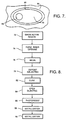
- FIG. 7 A plan view of the rear cell face in the via vicinity, for the embodiments of either FIGs. 5a-5c or FIG. 6, is shown in FIG. 7.
- the back via opening 66 is surrounded by the via metallization 68, which extends through the via and expands along the back side of the cell into a contact pad 70. All of the back via metallization, including the contact pad 70, is insulated from the back cell surface by the dielectric layer (not shown).
- the back face metallic contact sheet 56 surrounds the via metallization, but is spaced back from the metallization to avoid any electrical contact with it.
- a back cell contact can be formed at any convenient location on the back face sheet 56.
- FIG. 8 is a process flow diagram that summarizes a fabrication technique for the beveled via structure shown in FIG. 6.
- the active region is grown upon the semiconductor substrate and doped to establish the basic photocell.
- the active region may then be masked if desired. However, this is normally not necessary because no smoothing of the via opening, with the attendant aggressive etchants, is required.
- the substrate may also be thinned if desired to reduce the final cell weight.
- the inner opening 50 is next formed through the entire cell, including both the active layer and substrate, in step 74. It is formed either by mechanically grinding or drilling, or by laser scribing. A round cutting head is then used to produce a bevel on each side of the cell, connected by the inner opening 50, in step 76. If a mask has previously been formed over the active layer, it would be removed when the bevels have been completed.
- the dielectric is next deposited over the via opening in step 78. As described above, this can be performed either by dripping, dropper application, screen printing or in some other convenient manner. When the dielectric is initially deposited it bridges entirely across the inner opening to close the via. This is indicated by dashed lines 80 in FIG. 6.
- the dielectric is then cured in step 82, followed by the formation of an opening through the dielectric bridge in step 84.
- This opening is preferably established in a laser scribe operation with a laser focused to about 0.025mm, and as described above is used to produce a dielectric opening about 0.25mm in diameter.
- the via metallization is next laid down. This is performed by first covering the entire cell, except for those areas in which the metallization is desired, with a layer of photoresist in step 86.
- the photoresist pattern preferably exposes areas for both the front and back contact metallizations at the same time as the via metallization.
- the metal is then evaporated onto the cell in step 88, followed by lifting off the photoresist and the overlying metallization in step 90.
- the functional solar cell is now complete. If multiple cells have been formed on a common wafer, the individual cells are now diced and tested.
- the active region is grown prior to formation of the via opening, without having to worry about protecting the active region from chemical etchants previously used to smooth the via opening.
- the active region could be grown after the via has been formed. In this case it would generally be desirable to mask the substrate surface to prevent damaging it during the via processing. Such a mask need provide only mechanical protection for the substrate surface, since there are no strong etchants used which can degrade the mask.
- the resulting via structure results in a substantial improvement in leakage resistance, compared to prior coplanar contact solar cell designs.
- via design of FIG. 6 and a GaAs/Ge cell with a polyimide coating about 2 microns thick in the beveled areas average efficiencies of about 17% and a peak efficiency of about 18.5% were measured at AM (air mass) zero, 28°C.
- AM air mass
- the measured leakage resistance of applicants' test devices averaged 2 megohms, which is much greater than the 300 ohms resistance typical of conventional vias.
- the lowest measured resistance value of the test devices was 360 ohms, which is still high enough to maintain losses at less than 0.7%.
- the test devices were also found to have a high mechanical integrity and substantially greater than average pull strength for welded on copper tabs.
- an electrical via structure and fabrication method that is particularly suited to coplanar contact solar cells, wherein an initial opening 38, 48a, 48b through the substrate is coated and substantially closed with a dielectric material 42, 52, 80. An inner opening 44 is then formed through the dielectric , and the via is provided with a conductive coating 46, 54.
- the dielectric is initially applied in a liquid state and is thereafter cured to a solid. The need for strong chemical etchants to smooth the via opening prior to application of the dielectric and metallization is eliminated, and a polyimide dielectric on a GaAs/Ge solar cell has resulted in a substantial improvement in leakage resistance and cell efficiency.
Landscapes
- Engineering & Computer Science (AREA)
- Manufacturing & Machinery (AREA)
- Microelectronics & Electronic Packaging (AREA)
- Photovoltaic Devices (AREA)
Applications Claiming Priority (2)
| Application Number | Priority Date | Filing Date | Title |
|---|---|---|---|
| US751364 | 1991-08-19 | ||
| US07/751,364 US5425816A (en) | 1991-08-19 | 1991-08-19 | Electrical feedthrough structure and fabrication method |
Publications (3)
| Publication Number | Publication Date |
|---|---|
| EP0528311A2 true EP0528311A2 (de) | 1993-02-24 |
| EP0528311A3 EP0528311A3 (en) | 1993-03-03 |
| EP0528311B1 EP0528311B1 (de) | 1997-01-08 |
Family
ID=25021661
Family Applications (1)
| Application Number | Title | Priority Date | Filing Date |
|---|---|---|---|
| EP92113566A Expired - Lifetime EP0528311B1 (de) | 1991-08-19 | 1992-08-08 | Elektrische Durchführungsstruktur und Herstellungsverfahren |
Country Status (6)
| Country | Link |
|---|---|
| US (1) | US5425816A (de) |
| EP (1) | EP0528311B1 (de) |
| JP (1) | JPH05326991A (de) |
| AU (1) | AU648921B2 (de) |
| DE (1) | DE69216502T2 (de) |
| ES (1) | ES2095991T3 (de) |
Cited By (14)
| Publication number | Priority date | Publication date | Assignee | Title |
|---|---|---|---|---|
| DE19634617A1 (de) * | 1996-02-08 | 1997-08-14 | Mitsubishi Electric Corp | Solarzelle |
| EP2068369A1 (de) * | 2007-12-03 | 2009-06-10 | Interuniversitair Microelektronica Centrum (IMEC) | Photovoltaikzellen mit Metal-Wrap-Through und verbesserter Passivierung |
| WO2011015432A1 (de) * | 2009-08-03 | 2011-02-10 | Robert Bosch Gmbh | Sensorelement mit durchkontaktierloch |
| EP1995792A3 (de) * | 2007-05-22 | 2011-04-20 | Sanyo Electric Co., Ltd. | Solarzelle und Herstellungsverfahren dafür |
| NL2004698C2 (en) * | 2010-05-11 | 2011-11-15 | Stichting Energie | Solar cell and method of manufacturing such a solar cell. |
| WO2011142666A1 (en) * | 2010-05-11 | 2011-11-17 | Stichting Energieonderzoek Centrum Nederland | Solar cell and method of manufacturing such a solar cell |
| NL2005261C2 (en) * | 2010-08-24 | 2012-02-27 | Solland Solar Cells B V | Back contacted photovoltaic cell with an improved shunt resistance. |
| TWI505490B (zh) * | 2013-05-24 | 2015-10-21 | Reflective solar cells with high thermal conductivity | |
| EP3787046A1 (de) * | 2019-08-29 | 2021-03-03 | AZUR SPACE Solar Power GmbH | Stapelförmige mehrfachsolarzelle mit einem dielektrischen isolationsschichtsystem |
| EP3787043A1 (de) * | 2019-08-29 | 2021-03-03 | AZUR SPACE Solar Power GmbH | Passivierungsverfahren für ein durchgangsloch einer halbleiterscheibe |
| EP3787039A1 (de) * | 2019-08-29 | 2021-03-03 | AZUR SPACE Solar Power GmbH | Schutzverfahren für durchgangsöffnungen einer halbleiterscheibe |
| EP3787042A1 (de) * | 2019-08-29 | 2021-03-03 | AZUR SPACE Solar Power GmbH | Mehrfachsolarzelle mit rückseitenkontaktierter vorderseite |
| EP4053919A1 (de) * | 2021-03-02 | 2022-09-07 | AZUR SPACE Solar Power GmbH | Verfahren zum durchkontaktieren |
| EP4053920A1 (de) * | 2021-03-02 | 2022-09-07 | AZUR SPACE Solar Power GmbH | Solarzellenkontaktanordnung |
Families Citing this family (49)
| Publication number | Priority date | Publication date | Assignee | Title |
|---|---|---|---|---|
| US5620904A (en) * | 1996-03-15 | 1997-04-15 | Evergreen Solar, Inc. | Methods for forming wraparound electrical contacts on solar cells |
| US6405431B1 (en) | 1996-06-27 | 2002-06-18 | Samsung Electro-Mechanics Co., Ltd. | Method for manufacturing build-up multi-layer printed circuit board by using yag laser |
| US5762720A (en) * | 1996-06-27 | 1998-06-09 | Evergreen Solar, Inc. | Solar cell modules with integral mounting structure and methods for forming same |
| US5741370A (en) * | 1996-06-27 | 1998-04-21 | Evergreen Solar, Inc. | Solar cell modules with improved backskin and methods for forming same |
| US5986203A (en) * | 1996-06-27 | 1999-11-16 | Evergreen Solar, Inc. | Solar cell roof tile and method of forming same |
| US6278053B1 (en) * | 1997-03-25 | 2001-08-21 | Evergreen Solar, Inc. | Decals and methods for providing an antireflective coating and metallization on a solar cell |
| US6187448B1 (en) | 1997-07-24 | 2001-02-13 | Evergreen Solar, Inc. | Encapsulant material for solar cell module and laminated glass applications |
| US6114046A (en) * | 1997-07-24 | 2000-09-05 | Evergreen Solar, Inc. | Encapsulant material for solar cell module and laminated glass applications |
| US5970168A (en) * | 1997-08-05 | 1999-10-19 | Kla-Tencor Corporation | Fourier filtering mechanism for inspecting wafers |
| US6320116B1 (en) | 1997-09-26 | 2001-11-20 | Evergreen Solar, Inc. | Methods for improving polymeric materials for use in solar cell applications |
| US6077722A (en) * | 1998-07-14 | 2000-06-20 | Bp Solarex | Producing thin film photovoltaic modules with high integrity interconnects and dual layer contacts |
| US6215130B1 (en) * | 1998-08-20 | 2001-04-10 | Lucent Technologies Inc. | Thin film transistors |
| US6221769B1 (en) * | 1999-03-05 | 2001-04-24 | International Business Machines Corporation | Method for integrated circuit power and electrical connections via through-wafer interconnects |
| US6935023B2 (en) | 2000-03-08 | 2005-08-30 | Hewlett-Packard Development Company, L.P. | Method of forming electrical connection for fluid ejection device |
| US6711814B2 (en) * | 2000-06-19 | 2004-03-30 | Robinson Nugent, Inc. | Method of making printed circuit board having inductive vias |
| US6833615B2 (en) * | 2000-12-29 | 2004-12-21 | Intel Corporation | Via-in-pad with off-center geometry |
| US6659592B2 (en) | 2001-08-16 | 2003-12-09 | Hewlett-Packard Development Company, L.P. | Multiple redundant through hole electrical interconnects and method for forming the same |
| US6531653B1 (en) * | 2001-09-11 | 2003-03-11 | The Boeing Company | Low cost high solar flux photovoltaic concentrator receiver |
| US6902872B2 (en) | 2002-07-29 | 2005-06-07 | Hewlett-Packard Development Company, L.P. | Method of forming a through-substrate interconnect |
| US6716737B2 (en) | 2002-07-29 | 2004-04-06 | Hewlett-Packard Development Company, L.P. | Method of forming a through-substrate interconnect |
| US6790775B2 (en) * | 2002-10-31 | 2004-09-14 | Hewlett-Packard Development Company, L.P. | Method of forming a through-substrate interconnect |
| US7335835B2 (en) * | 2002-11-08 | 2008-02-26 | The Boeing Company | Solar cell structure with by-pass diode and wrapped front-side diode interconnection |
| US7170001B2 (en) * | 2003-06-26 | 2007-01-30 | Advent Solar, Inc. | Fabrication of back-contacted silicon solar cells using thermomigration to create conductive vias |
| US7649141B2 (en) * | 2003-06-30 | 2010-01-19 | Advent Solar, Inc. | Emitter wrap-through back contact solar cells on thin silicon wafers |
| US20050172996A1 (en) * | 2004-02-05 | 2005-08-11 | Advent Solar, Inc. | Contact fabrication of emitter wrap-through back contact silicon solar cells |
| US7335555B2 (en) * | 2004-02-05 | 2008-02-26 | Advent Solar, Inc. | Buried-contact solar cells with self-doping contacts |
| US7144751B2 (en) * | 2004-02-05 | 2006-12-05 | Advent Solar, Inc. | Back-contact solar cells and methods for fabrication |
| US20060060238A1 (en) * | 2004-02-05 | 2006-03-23 | Advent Solar, Inc. | Process and fabrication methods for emitter wrap through back contact solar cells |
| US20050275057A1 (en) * | 2004-06-15 | 2005-12-15 | Breen Marc L | Schottky diode with dielectric isolation |
| US7331163B2 (en) * | 2004-10-29 | 2008-02-19 | Hau Joseph A | Refrigerator with integral vacuum sealer |
| CA2568136C (en) * | 2006-11-30 | 2008-07-29 | Tenxc Wireless Inc. | Butler matrix implementation |
| WO2008076879A1 (en) * | 2006-12-15 | 2008-06-26 | Evergreen Solar, Inc. | Plug-together photovoltaic modules |
| US20080216887A1 (en) * | 2006-12-22 | 2008-09-11 | Advent Solar, Inc. | Interconnect Technologies for Back Contact Solar Cells and Modules |
| US20080185038A1 (en) * | 2007-02-02 | 2008-08-07 | Emcore Corporation | Inverted metamorphic solar cell with via for backside contacts |
| US8034702B2 (en) | 2007-08-16 | 2011-10-11 | Micron Technology, Inc. | Methods of forming through substrate interconnects |
| WO2009064870A2 (en) * | 2007-11-13 | 2009-05-22 | Advent Solar, Inc. | Selective emitter and texture processes for back contact solar cells |
| JP2009135338A (ja) * | 2007-11-30 | 2009-06-18 | Sanyo Electric Co Ltd | 太陽電池及び太陽電池の製造方法 |
| JP5259197B2 (ja) * | 2008-01-09 | 2013-08-07 | ソニー株式会社 | 半導体装置及びその製造方法 |
| CN102113130A (zh) * | 2008-04-29 | 2011-06-29 | 应用材料股份有限公司 | 使用单石模块组合技术制造的光伏打模块 |
| US20090277503A1 (en) * | 2008-05-10 | 2009-11-12 | Solfocus, Inc. | Solar Cell with Current Blocking Layer |
| US8852994B2 (en) | 2010-05-24 | 2014-10-07 | Masimo Semiconductor, Inc. | Method of fabricating bifacial tandem solar cells |
| US8525343B2 (en) * | 2010-09-28 | 2013-09-03 | Taiwan Semiconductor Manufacturing Company, Ltd. | Device with through-silicon via (TSV) and method of forming the same |
| DE102010060303A1 (de) | 2010-11-02 | 2012-05-03 | Solarworld Innovations Gmbh | Verfahren zum Herstellen einer Solarzelle |
| US8894868B2 (en) | 2011-10-06 | 2014-11-25 | Electro Scientific Industries, Inc. | Substrate containing aperture and methods of forming the same |
| FR2983346B1 (fr) * | 2011-11-25 | 2016-12-09 | Soitec Silicon On Insulator | Procede de prevention d'une panne electrique dans un empilement de couches semi-conductrices, cellule photovoltaïque a concentration a substrat mince, et assemblage de cellule solaire |
| US9680035B1 (en) * | 2016-05-27 | 2017-06-13 | Solar Junction Corporation | Surface mount solar cell with integrated coverglass |
| US20240074054A1 (en) * | 2022-08-25 | 2024-02-29 | The Phoenix Company Of Chicago, Inc. | Impedance matched via connections in a printed circuit board |
| DE102023002413A1 (de) | 2023-06-14 | 2024-12-19 | Azur Space Solar Power Gmbh | Verfahren zur Herstellung eines Vias bei einer III-V Mehrfachsolarzelle |
| DE102023002414A1 (de) | 2023-06-14 | 2024-12-19 | Azur Space Solar Power Gmbh | Verfahren zur Herstellung eines Grabens bei einer III-V Mehrfachsolarzelle |
Family Cites Families (17)
| Publication number | Priority date | Publication date | Assignee | Title |
|---|---|---|---|---|
| JPS4892879A (de) * | 1972-03-09 | 1973-12-01 | ||
| DE2453788A1 (de) * | 1973-11-21 | 1975-05-22 | Litton Industries Inc | Verfahren zur herstellung von schaltplatten mit gedruckten schaltungen |
| US3903427A (en) * | 1973-12-28 | 1975-09-02 | Hughes Aircraft Co | Solar cell connections |
| JPS5412376A (en) * | 1977-06-25 | 1979-01-30 | Yoshitomi Pharmaceut Ind Ltd | Antibacterial derivative of pseudomonic acid |
| JPS5567182A (en) * | 1978-11-15 | 1980-05-21 | Nippon Electric Co | Heat transmitting printed circuit board |
| JPS60236280A (ja) * | 1984-05-10 | 1985-11-25 | 松下電工株式会社 | 配線用板 |
| US4601916A (en) * | 1984-07-18 | 1986-07-22 | Kollmorgen Technologies Corporation | Process for bonding metals to electrophoretically deposited resin coatings |
| JPS61248496A (ja) * | 1985-04-25 | 1986-11-05 | オ−ケ−プリント配線株式会社 | フレキシブル基板装置 |
| JPS61292379A (ja) * | 1985-06-19 | 1986-12-23 | Sharp Corp | ラツパラウンドコンタクトセル |
| US4791248A (en) * | 1987-01-22 | 1988-12-13 | The Boeing Company | Printed wire circuit board and its method of manufacture |
| JPS63211773A (ja) * | 1987-02-27 | 1988-09-02 | Mitsubishi Electric Corp | 化合物半導体太陽電池 |
| JPS6482570A (en) * | 1987-09-24 | 1989-03-28 | Mitsubishi Electric Corp | Manufacture of photoelectric conversion device |
| JPH0691303B2 (ja) * | 1987-11-30 | 1994-11-14 | イビデン株式会社 | 電子部品搭載プリント配線板装置 |
| WO1989005521A1 (en) * | 1987-12-03 | 1989-06-15 | Spectrolab, Inc. | Solar cell panel |
| US4981525A (en) * | 1988-02-19 | 1991-01-01 | Sanyo Electric Co., Ltd. | Photovoltaic device |
| JPH0298974A (ja) * | 1988-10-05 | 1990-04-11 | Sanyo Electric Co Ltd | 光起電力装置の製造方法 |
| JP2773366B2 (ja) * | 1990-03-19 | 1998-07-09 | 富士通株式会社 | 多層配線基板の形成方法 |
-
1991
- 1991-08-19 US US07/751,364 patent/US5425816A/en not_active Expired - Lifetime
-
1992
- 1992-08-07 AU AU20907/92A patent/AU648921B2/en not_active Ceased
- 1992-08-08 EP EP92113566A patent/EP0528311B1/de not_active Expired - Lifetime
- 1992-08-08 ES ES92113566T patent/ES2095991T3/es not_active Expired - Lifetime
- 1992-08-08 DE DE69216502T patent/DE69216502T2/de not_active Expired - Fee Related
- 1992-08-18 JP JP4218055A patent/JPH05326991A/ja active Pending
Cited By (27)
| Publication number | Priority date | Publication date | Assignee | Title |
|---|---|---|---|---|
| DE19634617B4 (de) * | 1996-02-08 | 2007-06-14 | Mitsubishi Denki K.K. | Verfahren zur Herstellung einer Siliziumsolarzelle mit verringerter Rekombination nahe der Solarzellenoberfläche |
| DE19634617A1 (de) * | 1996-02-08 | 1997-08-14 | Mitsubishi Electric Corp | Solarzelle |
| EP1995792A3 (de) * | 2007-05-22 | 2011-04-20 | Sanyo Electric Co., Ltd. | Solarzelle und Herstellungsverfahren dafür |
| EP2068369A1 (de) * | 2007-12-03 | 2009-06-10 | Interuniversitair Microelektronica Centrum (IMEC) | Photovoltaikzellen mit Metal-Wrap-Through und verbesserter Passivierung |
| WO2009071561A2 (en) | 2007-12-03 | 2009-06-11 | Interuniversitair Microelektronica Centrum Vzw | Photovoltaic cells having metal wrap through and improved passivation |
| WO2009071561A3 (en) * | 2007-12-03 | 2009-12-10 | Imec | Photovoltaic cells having metal wrap through and improved passivation |
| US9246044B2 (en) | 2007-12-03 | 2016-01-26 | Imec | Photovoltaic cells having metal wrap through and improved passivation |
| CN102474990A (zh) * | 2009-08-03 | 2012-05-23 | 罗伯特·博世有限公司 | 具有层间连接孔的传感器元件 |
| WO2011015432A1 (de) * | 2009-08-03 | 2011-02-10 | Robert Bosch Gmbh | Sensorelement mit durchkontaktierloch |
| CN102474990B (zh) * | 2009-08-03 | 2015-11-25 | 罗伯特·博世有限公司 | 具有层间连接孔的传感器元件 |
| US8883539B2 (en) | 2010-05-11 | 2014-11-11 | Stichting Energieonderzoek Centrum Nederland | Solar cell and method of its manufacture |
| WO2011142666A1 (en) * | 2010-05-11 | 2011-11-17 | Stichting Energieonderzoek Centrum Nederland | Solar cell and method of manufacturing such a solar cell |
| NL2004698C2 (en) * | 2010-05-11 | 2011-11-15 | Stichting Energie | Solar cell and method of manufacturing such a solar cell. |
| WO2012026812A1 (en) * | 2010-08-24 | 2012-03-01 | Solland Solar Energy Holding B.V. | Back contacted photovoltaic cell with an improved shunt resistance. |
| NL2005261C2 (en) * | 2010-08-24 | 2012-02-27 | Solland Solar Cells B V | Back contacted photovoltaic cell with an improved shunt resistance. |
| US9368656B2 (en) | 2010-08-24 | 2016-06-14 | Stichting Energieonderzoek Centrum Nederland | Back contacted photovoltaic cell with an improved shunt resistance |
| TWI505490B (zh) * | 2013-05-24 | 2015-10-21 | Reflective solar cells with high thermal conductivity | |
| EP3787039A1 (de) * | 2019-08-29 | 2021-03-03 | AZUR SPACE Solar Power GmbH | Schutzverfahren für durchgangsöffnungen einer halbleiterscheibe |
| EP3787043A1 (de) * | 2019-08-29 | 2021-03-03 | AZUR SPACE Solar Power GmbH | Passivierungsverfahren für ein durchgangsloch einer halbleiterscheibe |
| EP3787046A1 (de) * | 2019-08-29 | 2021-03-03 | AZUR SPACE Solar Power GmbH | Stapelförmige mehrfachsolarzelle mit einem dielektrischen isolationsschichtsystem |
| EP3787042A1 (de) * | 2019-08-29 | 2021-03-03 | AZUR SPACE Solar Power GmbH | Mehrfachsolarzelle mit rückseitenkontaktierter vorderseite |
| US11081615B2 (en) | 2019-08-29 | 2021-08-03 | Azur Space Solar Power Gmbh | Protection method for through-holes of a semiconductor wafer |
| US11640998B2 (en) | 2019-08-29 | 2023-05-02 | Azur Space Solar Power Gmbh | Multi-junction solar cell with back-contacted front side |
| US11837672B2 (en) | 2019-08-29 | 2023-12-05 | Azur Space Solar Power Gmbh | Stacked multijunction solar cell having a dielectric insulating layer system |
| US12628461B2 (en) | 2019-08-29 | 2026-05-12 | Azur Space Solar Power Gmbh | Passivation method for a passage opening of a wafer |
| EP4053919A1 (de) * | 2021-03-02 | 2022-09-07 | AZUR SPACE Solar Power GmbH | Verfahren zum durchkontaktieren |
| EP4053920A1 (de) * | 2021-03-02 | 2022-09-07 | AZUR SPACE Solar Power GmbH | Solarzellenkontaktanordnung |
Also Published As
| Publication number | Publication date |
|---|---|
| DE69216502T2 (de) | 1997-04-24 |
| US5425816A (en) | 1995-06-20 |
| JPH05326991A (ja) | 1993-12-10 |
| EP0528311B1 (de) | 1997-01-08 |
| AU2090792A (en) | 1993-02-25 |
| EP0528311A3 (en) | 1993-03-03 |
| ES2095991T3 (es) | 1997-03-01 |
| DE69216502D1 (de) | 1997-02-20 |
| AU648921B2 (en) | 1994-05-05 |
Similar Documents
| Publication | Publication Date | Title |
|---|---|---|
| US5425816A (en) | Electrical feedthrough structure and fabrication method | |
| US5133810A (en) | Flexible photovoltaic device and manufacturing method thereof | |
| CN100524832C (zh) | 太阳能电池背接触上的导电层的接触隔离方法和相应的太阳能电池 | |
| US5580395A (en) | Solar cell with integrated bypass function | |
| KR101484355B1 (ko) | 단결정 태양 전지의 제조 방법 | |
| EP0427934A2 (de) | Monolithisches Modul mit serien- und parallel-angeschalteten photovoltaischen Zellen | |
| KR100526445B1 (ko) | 웨이퍼 패시베이션 구조 | |
| JP5926547B2 (ja) | 半導体デバイスパッケージ | |
| US20040261834A1 (en) | Chain link metal interconnect structure | |
| EP0641487A1 (de) | Monolithische parallelgeschaltete photovoltaische anordnung und herstellungsverfahren. | |
| WO2001033639A1 (en) | Formation of contacts on thin films | |
| US3436611A (en) | Insulation structure for crossover leads in integrated circuitry | |
| US6417442B1 (en) | Solar battery assembly and method of forming a solar battery assembly | |
| US4156309A (en) | Method of construction of a multi-cell solar array | |
| KR100435137B1 (ko) | 두꺼운도체를갖는모노리식마이크로파집적회로를제조하는방법 | |
| US3408271A (en) | Electrolytic plating of metal bump contacts to semiconductor devices upon nonconductive substrates | |
| US5932926A (en) | Microwave semiconductor integrated circuit | |
| JPS5839073A (ja) | アモルフアス太陽電池 | |
| US5500377A (en) | Method of making surge suppressor switching device | |
| US20090155994A1 (en) | Forming thin film transistors using ablative films with pre-patterned conductors | |
| CA1209281A (en) | Multi-level aluminum metallization structure for semiconductor device | |
| US20220285567A1 (en) | Method for through-hole plating | |
| JP3261278B2 (ja) | インターコネクタ付ダイオードの製造方法 | |
| JPH0653377A (ja) | ダイオード | |
| JPS63275142A (ja) | 半導体装置の製造方法 |
Legal Events
| Date | Code | Title | Description |
|---|---|---|---|
| PUAI | Public reference made under article 153(3) epc to a published international application that has entered the european phase |
Free format text: ORIGINAL CODE: 0009012 |
|
| PUAL | Search report despatched |
Free format text: ORIGINAL CODE: 0009013 |
|
| AK | Designated contracting states |
Kind code of ref document: A2 Designated state(s): DE ES FR GB IT |
|
| AK | Designated contracting states |
Kind code of ref document: A3 Designated state(s): DE ES FR GB IT |
|
| 17P | Request for examination filed |
Effective date: 19930824 |
|
| 17Q | First examination report despatched |
Effective date: 19941206 |
|
| GRAG | Despatch of communication of intention to grant |
Free format text: ORIGINAL CODE: EPIDOS AGRA |
|
| GRAH | Despatch of communication of intention to grant a patent |
Free format text: ORIGINAL CODE: EPIDOS IGRA |
|
| GRAH | Despatch of communication of intention to grant a patent |
Free format text: ORIGINAL CODE: EPIDOS IGRA |
|
| GRAA | (expected) grant |
Free format text: ORIGINAL CODE: 0009210 |
|
| AK | Designated contracting states |
Kind code of ref document: B1 Designated state(s): DE ES FR GB IT |
|
| REF | Corresponds to: |
Ref document number: 69216502 Country of ref document: DE Date of ref document: 19970220 |
|
| REG | Reference to a national code |
Ref country code: ES Ref legal event code: FG2A Ref document number: 2095991 Country of ref document: ES Kind code of ref document: T3 |
|
| ET | Fr: translation filed | ||
| ITF | It: translation for a ep patent filed | ||
| PGFP | Annual fee paid to national office [announced via postgrant information from national office to epo] |
Ref country code: FR Payment date: 19970710 Year of fee payment: 6 |
|
| PGFP | Annual fee paid to national office [announced via postgrant information from national office to epo] |
Ref country code: GB Payment date: 19970717 Year of fee payment: 6 |
|
| PGFP | Annual fee paid to national office [announced via postgrant information from national office to epo] |
Ref country code: DE Payment date: 19970723 Year of fee payment: 6 |
|
| PGFP | Annual fee paid to national office [announced via postgrant information from national office to epo] |
Ref country code: ES Payment date: 19970812 Year of fee payment: 6 |
|
| PLBE | No opposition filed within time limit |
Free format text: ORIGINAL CODE: 0009261 |
|
| 26N | No opposition filed | ||
| PG25 | Lapsed in a contracting state [announced via postgrant information from national office to epo] |
Ref country code: GB Free format text: LAPSE BECAUSE OF NON-PAYMENT OF DUE FEES Effective date: 19980808 |
|
| PG25 | Lapsed in a contracting state [announced via postgrant information from national office to epo] |
Ref country code: ES Free format text: LAPSE BECAUSE OF THE APPLICANT RENOUNCES Effective date: 19980810 |
|
| GBPC | Gb: european patent ceased through non-payment of renewal fee |
Effective date: 19980808 |
|
| PG25 | Lapsed in a contracting state [announced via postgrant information from national office to epo] |
Ref country code: FR Free format text: LAPSE BECAUSE OF NON-PAYMENT OF DUE FEES Effective date: 19990430 |
|
| PG25 | Lapsed in a contracting state [announced via postgrant information from national office to epo] |
Ref country code: DE Free format text: LAPSE BECAUSE OF NON-PAYMENT OF DUE FEES Effective date: 19990601 |
|
| REG | Reference to a national code |
Ref country code: FR Ref legal event code: ST |
|
| REG | Reference to a national code |
Ref country code: ES Ref legal event code: FD2A Effective date: 20001102 |
|
| PG25 | Lapsed in a contracting state [announced via postgrant information from national office to epo] |
Ref country code: IT Free format text: LAPSE BECAUSE OF NON-PAYMENT OF DUE FEES;WARNING: LAPSES OF ITALIAN PATENTS WITH EFFECTIVE DATE BEFORE 2007 MAY HAVE OCCURRED AT ANY TIME BEFORE 2007. THE CORRECT EFFECTIVE DATE MAY BE DIFFERENT FROM THE ONE RECORDED. Effective date: 20050808 |