EP0530554A2 - Schrubben und Ersetzen in einem Speichersystem - Google Patents
Schrubben und Ersetzen in einem Speichersystem Download PDFInfo
- Publication number
- EP0530554A2 EP0530554A2 EP92113738A EP92113738A EP0530554A2 EP 0530554 A2 EP0530554 A2 EP 0530554A2 EP 92113738 A EP92113738 A EP 92113738A EP 92113738 A EP92113738 A EP 92113738A EP 0530554 A2 EP0530554 A2 EP 0530554A2
- Authority
- EP
- European Patent Office
- Prior art keywords
- memory
- data word
- chip
- memory chip
- uncorrected data
- Prior art date
- Legal status (The legal status is an assumption and is not a legal conclusion. Google has not performed a legal analysis and makes no representation as to the accuracy of the status listed.)
- Withdrawn
Links
Images


Classifications
-
- G—PHYSICS
- G11—INFORMATION STORAGE
- G11C—STATIC STORES
- G11C29/00—Checking stores for correct operation ; Subsequent repair; Testing stores during standby or offline operation
- G11C29/70—Masking faults in memories by using spares or by reconfiguring
-
- G—PHYSICS
- G06—COMPUTING OR CALCULATING; COUNTING
- G06F—ELECTRIC DIGITAL DATA PROCESSING
- G06F11/00—Error detection; Error correction; Monitoring
- G06F11/07—Responding to the occurrence of a fault, e.g. fault tolerance
- G06F11/0703—Error or fault processing not based on redundancy, i.e. by taking additional measures to deal with the error or fault not making use of redundancy in operation, in hardware, or in data representation
- G06F11/0706—Error or fault processing not based on redundancy, i.e. by taking additional measures to deal with the error or fault not making use of redundancy in operation, in hardware, or in data representation the processing taking place on a specific hardware platform or in a specific software environment
- G06F11/0721—Error or fault processing not based on redundancy, i.e. by taking additional measures to deal with the error or fault not making use of redundancy in operation, in hardware, or in data representation the processing taking place on a specific hardware platform or in a specific software environment within a central processing unit [CPU]
- G06F11/0724—Error or fault processing not based on redundancy, i.e. by taking additional measures to deal with the error or fault not making use of redundancy in operation, in hardware, or in data representation the processing taking place on a specific hardware platform or in a specific software environment within a central processing unit [CPU] in a multiprocessor or a multi-core unit
-
- G—PHYSICS
- G06—COMPUTING OR CALCULATING; COUNTING
- G06F—ELECTRIC DIGITAL DATA PROCESSING
- G06F11/00—Error detection; Error correction; Monitoring
- G06F11/07—Responding to the occurrence of a fault, e.g. fault tolerance
- G06F11/0703—Error or fault processing not based on redundancy, i.e. by taking additional measures to deal with the error or fault not making use of redundancy in operation, in hardware, or in data representation
- G06F11/0751—Error or fault detection not based on redundancy
- G06F11/0754—Error or fault detection not based on redundancy by exceeding limits
- G06F11/076—Error or fault detection not based on redundancy by exceeding limits by exceeding a count or rate limit, e.g. word- or bit count limit
-
- G—PHYSICS
- G06—COMPUTING OR CALCULATING; COUNTING
- G06F—ELECTRIC DIGITAL DATA PROCESSING
- G06F11/00—Error detection; Error correction; Monitoring
- G06F11/07—Responding to the occurrence of a fault, e.g. fault tolerance
- G06F11/08—Error detection or correction by redundancy in data representation, e.g. by using checking codes
- G06F11/10—Adding special bits or symbols to the coded information, e.g. parity check, casting out 9's or 11's
- G06F11/1008—Adding special bits or symbols to the coded information, e.g. parity check, casting out 9's or 11's in individual solid state devices
- G06F11/1012—Adding special bits or symbols to the coded information, e.g. parity check, casting out 9's or 11's in individual solid state devices using codes or arrangements adapted for a specific type of error
- G06F11/1024—Identification of the type of error
-
- G—PHYSICS
- G06—COMPUTING OR CALCULATING; COUNTING
- G06F—ELECTRIC DIGITAL DATA PROCESSING
- G06F11/00—Error detection; Error correction; Monitoring
- G06F11/07—Responding to the occurrence of a fault, e.g. fault tolerance
- G06F11/08—Error detection or correction by redundancy in data representation, e.g. by using checking codes
- G06F11/10—Adding special bits or symbols to the coded information, e.g. parity check, casting out 9's or 11's
- G06F11/1008—Adding special bits or symbols to the coded information, e.g. parity check, casting out 9's or 11's in individual solid state devices
- G06F11/1048—Adding special bits or symbols to the coded information, e.g. parity check, casting out 9's or 11's in individual solid state devices using arrangements adapted for a specific error detection or correction feature
- G06F11/106—Correcting systematically all correctable errors, i.e. scrubbing
-
- G—PHYSICS
- G06—COMPUTING OR CALCULATING; COUNTING
- G06F—ELECTRIC DIGITAL DATA PROCESSING
- G06F2201/00—Indexing scheme relating to error detection, to error correction, and to monitoring
- G06F2201/88—Monitoring involving counting
Definitions
- the present invention relates to computer memory systems and a method according to the preamble of claim 1 or 2 respectively.
- the data word may comprise 72 bit positions where 64 positions store data and 8 positions are employed for an error correcting check byte which, when processed by a suitable error correcting system associated with the memory, is capable of automatically correcting a single-bit error in any one of the bit positions of the word.
- Most systems also are capable of detecting multi-bit errors and are generally designed from a code standpoint so as not to miscorrect any of the good data bits.
- the prior art also includes systems for correcting double bit errors.
- An article entitled “MULTIPLE ERROR CORRECTION” (IBM Technical Disclosure Bulletin, Vol. 13, No. 8, January 1971, Pg. 2190) describes a circuit for automatically correcting multiple bit errors.
- the word fetched from memory is read into an error register and the complement of the fetched word is rewritten back into the original memory location.
- a fetch cycle is then executed on the complement of the fetched word.
- the word and its complement arc compared in an Exclusive OR circuit that identifies the location of the failing bits. This information is utilized to complement the incorrect bits in the original fetched word.
- the information concerning the failing bits is also stored with the address position of the error.
- scrubbing In order to correct soft errors that tend to occur in the memory array between refresh cycles, many conventional systems implement a technique known as "scrubbing". During a scrubbing cycle, each memory location in an array is accessed sequentially and the data within is read. Typically, ECC logic checks each data word and corrects any single bit errors. The data is then restored to memory. If the single bit error was related to a soft error, the restore operation puts corrected data in place of the bad data that was the soft fail.
- Sparing also known as “bit-steering” refers to the replacement of an identified defective bit position by logically steering a bit from a replacement chip into the defective bit position, effectively replacing the defective position.
- bit-steering refers to the replacement of an identified defective bit position by logically steering a bit from a replacement chip into the defective bit position, effectively replacing the defective position.
- a storage system including improved scrubbing and sparing logic whereby the memory storage system is maintained by identifying and recording the number of hard errors on each memory chip.
- the system maintains a recording counter for each of the data bits in the ECC data word. When one of the counters is incremented beyond a predetermined threshold, the system invokes sparing to replace the failing bit position.
- a spare chip is specifically designated to replace a defective chip, the system continues to write to the defective chip in parallel with the spare chip even after bit steering has been invoked. This helps to ensure the reliability of data on the replacement chip in case it is accidentally brought off-line.
- the continuous updating of the contents of the replaced chip allows its functioning memory to be used as a partial backup for the replacement chip.
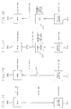
- Fig. 1 is a block diagram of a Central Electronic Complex (CEC) of a type conforming to IBM Enterprise Systems Architecture/390 (ESA/390).
- the CEC of Fig. 1 includes three Central Processors 102a-c.
- Each Central Processor (CP) has its own conventional first level high speed buffer (L1) 104a-c.
- the L1s are connected in turn to a second level high speed buffer (L2) 106 which is shared by all the CP's.
- the L2 106 is connected to Central Storage 108, also known as main storage, through a System Control Element (SCE) 118.
- SCE System Control Element
- the general term 'storage' is used to refer to data existing in either level high speed buffer (104a-c or 106) or the Central Storage 108 itself or any Main Storage Array (MSA) used for memory.
- the CEC of Fig. 1 also includes an Interconnect Communication Element (ICE) 110a which controls data transfer and communication between the SCE 118, an Expanded Storage (ES) 112 and a Channel Subsystem 110b.
- ICE 110a and Channel Subsystem 110b are also collectively referred to as the I/O Subsystem.
- System operations and support functions such as powering on and off and configuring the system are controlled by a support processor called the Processor Controller Element (PCE) 116.
- the PCE is also used to assist system elements in recovering from errors.
- the present invention can be used in conjunction with with any type of semiconductor storage array whether within the CEC environment of Fig. 1 or within other computer system environments.
- the invention will be described as applied to the Central Storage 108 in the system of Fig. 1.
- the Central Storage 108 includes one or more of Main Storage Arrays 202.
- the Main Storage Arrays 202 are of a conventional type comprising arrays of dynamic random access memory chips (DRAMS).
- DRAMS dynamic random access memory chips
- the number of chip rows per MSA is configuration dependent typically with one or two chip rows per MSA.
- each MSA reads/writes data in the form of two 72 bit ECC data words (144 bit quadword of data) simultaneously.
- Read/Write access and addressing of the Main Storage Arrays 202 is provided by conventional array control logic 204 which operates responsive to commands from a Memory Controller 206. Scrub operations use physical addresses without any absolute to physical address conversions normally done to other storage requests.
- the Memory Controller 206 provides the connections and control signals used by requestors to initiate accesses to the Central Storage 108. These signals service requests from the Hardware Assisted Memory Tester (HAMT) 208 whose function and operation will be described later. Additional connections 207 are provided to serve other requestors (such as the ICE 110A or L2 106) requiring conventional accesses to memory.
- HAMT Hardware Assisted Memory Tester
- MSA1 202 is connected to an input of a selective invert logic 210 by way of its own bidirectional data bus 212.
- the selective invert logic also has a second data input from a fetch buffer 214 (described in more detail later).
- the selective invert logic 210 can invert or pass through in uninverted (true) form, the data from either the MSA 202 or the fetch buffer 214.
- the control of which input to select and whether or not to invert the output of a selected MSA is provided by way of signals from the memory controller 206.
- the remaining MSAs (MSA 2 - MSA 4) are similarly connected, each to their own selective invert logics (each of which receives a second input from the fetch buffer 214). In operation, only the data from the MSA being scrubbed will be inverted.
- the output of the selective invert logic 210 is connected to ECC logic 216.
- the ECC logic is of the double bit error detect/single bit error correct type which is well known in the art.
- the ECC logic includes two separate ECC circuits for each MSA with a data path for data fed back from the fetch buffer 214.
- Each ECC logic 216 operates on the 144 bit quadwords as two individual 72 bit ECC data words, thus providing two separate and distinct eight bit ECCs (one for each 64 data bits in the ECC data word).
- the ECC logic 216 can be enabled or disabled (error correction turned on or off) by way of a signal from the Memory Controller 206. It should be understood that only the selective invert 210 and ECC logic 216 associated with MSA 1 has been shown for clarity.
- MSAs 2-4 are connected identically, each to their own duplicate copy of the selective invert logic and ECC logic which operate as described with respect to the identical logic supporting MSA 1. Thus there are four ECC logics in all, each separately controlled by the
- the four ECC logics 216 are connected to a fetch buffer 214.
- the fetch buffer is of a conventional type and provides temporary storage for 16 quad words (a double line of data) from a selected MSA (as addressed by the Memory Controller 206).
- the fetch buffer 214 latches in quadwords from the ECC logic under control of the Memory Controller 206.
- the output of the fetch buffer 214 (a quadword) is provided as an input to the selective invert logic 210 and as an input to compare and count logic 218.
- the fetch buffer 214 is also used in common by the SCE to provide data from the central storage to the L2 High Speed Buffer (the connection to the L2 buffer is not is not shown for clarity).
- the fetch buffer 214 there are many workable alternative embodiments for the fetch buffer 214.
- one common fetch buffer can be provided for all of the MSAs.
- two identical fetch buffers can be provided so as to handle requests in tandem.
- a separate fetch buffer can be provided for each MSA.
- the fetch buffer output is connected as an input to the selective invert logics for the MSAs and to the compare and count logic 218.
- the quadword output of the ECC logic 216 and the quadwords from each of the remaining three ECC logics associated with MSA 2-4 are also provided to a 4:1 multiplexer (4:1 MUX) 220.
- the 4:1 MUX 220 connects a selected one of the four quad words from the ECC logic to the compare and count logic 218. The selection of a quadword is made under control of signal lines from the Memory Controller 206.
- the compare and count logic 218 comprises two sets of components, a plurality of comparators 222 and a plurality of counters 224.
- the comparators comprise 144 comparators in all, one for each bit of the quadword. Each comparator is thus connected to compare a unique bit position in the quadword provided by the 4:1 MUX 220 with its counterpart provided by the fetch buffer 214.
- the comparators 222 compare each of the 144 bit positions in the quadword output from the 4:1 MUX with its counterpart in the quadword provided by the output of the fetch buffer 214, resulting in 144 comparison results.
- the counters 224 comprise 144 counters each being ten bits wide plus one parity bit. The 144 counters thus enable failures from every one of the 144 bit positions to be recorded. Each of the 144 counters represents one bit position in the quadword and is connected to receive the output from a different one of the 144 comparators 222.
- Each counter is of a type that will increment each time the connected comparator indicates that a corresponding bit position in the quadword from the fetch buffer 214 does not match its counterpart in the quadword selected via the 4:1 MUX 220.
- Each of the counters 224 can also be read out and written into as a shift register under control of the HAMT 208.
- the compare and increment functions of the compare and count logic 218 can be enabled and disabled by the Memory Controller 206 (which, in the present embodiment, enables these functions only during the scrub cycle).
- the Hardware Assisted Memory Tester (HAMT) 208 is a programmable memory tester which can be of any of a number of types well known in the art.
- a prior art memory tester also sometimes referred to as a storage validator
- U.S. Patent 4,342,084 to Sager et. al. which is incorporated by reference herein, in its entirety, as if printed in full below.
- the test/memory access programs generated by the HAMT are selected and configured under control of command words from the system console or PCE 116.
- the HAMT 208 also performs the function of sequencing scrubbing operations.
- the chip scrubbing operation is used to correct soft single bit errors in Central Storage 108 and is also used to record hard errors so that chip failure mechanisms affecting many bits can be detected and, if the replacement criteria has been met, to invoke the HAMT chip sparing logic.
- the scrub process is controlled by a HAMT Execution Control Word (HECW) that is loaded into an environmental reset type embedded array by the PCE 116 at initial machine loading (IML) time.
- the scrub HECW contains a byte for each of the high order address bytes of the two chip row starting addresses and a byte for each of the high order address bytes of the two chip row ending addresses.
- Internal HAMT logic supplies all other address information, including the MSA ID, for the scrub operations at the time the HECW register is loaded from the embedded array.
- the PCE console is also programmed to provide a programmable error threshold for the counters 224 and a programmable interval for the time between scrub cycles. The above-described information is provided to the HAMT 208 by the PCE 116.
- the HECW in the embedded array is read out and loaded into the a HAMT HECW register for execution. After the register is loaded, the current address is incremented to the next double line address if the trigger indicating the start of a new chip row address range is not set.
- the HECW current address is returned to the embedded array and held for the next scrub operation. This process is repeated for each chip row address range on one MSA and then for each MSA. When the entire memory has been scrubbed, the address controls wrap around and continue again.
- the programmable scrub interval is set so that all on-line memory storage will be scrubbed in approximately four minutes.
- HAMT sends 792 advances (read and increment commands) to the compare and count logic 218.
- the advances cause the contents of the 144 hard error counters 224 to be sent to HAMT on two single bit serial buses.
- Each bus is connected to a group of 72 counters thus enabling a bit from each of two counters to be read in at the same time.
- the first group of 72 counters are read in simultaneously with the other group of 72 counters.
- HAMT As the contents of the hard error counters are being read in, HAMT sends out to the counters zeroes with good parity. After HAMT has read in all counters they are in a reset state. As the counters are being read in, HAMT counts the number of bits received. At the completion of the process of reading in all counters, HAMT checks for a "sparing needed" condition as described below.
- the HAMT 208 compares the counter value to the threshold set in the PCE register. If the counter equals or exceeds the threshold, a HAMT internal bit is set to indicate sparing is needed and the position of the counter among the 72 counters is also remembered by HAMT. Only the first counter to equal or exceed the threshold per group of 72 counters gets remembered.
- each MSA comprises two of such memory cards, each handling storage of 72 bits of the 144 bit quadword.
- Each memory card comprises a plurality of Dynamic Random Access Memory chips (DRAMS) of a conventional type.
- DRAMS Dynamic Random Access Memory chips
- the DRAMS 502(1)-502(N) & 506 are 1 Meg X 4 bit types.
- Each of the DRAMS is connected to bit flow control logic 504(1)-504(N), 504(SP). The bit flow control logic selects one bit from each four bit set output/input by each of the DRAMS.
- the bit flow control logic and the DRAMS operate under control of the array control logic 204 which causes each DRAM in the array to behave as an 4 Meg X 1 bit chip.
- the first 72 DRAMS 502(1)-502(N) supply 72 of the 144 bits in the fetched quadword (this first set of 72 bits is referred to as the "even" addressed ECC data word). It should be understood that additional rows of chips can be added to provide each card with more memory.
- a spare DRAM chip 506 is identical to the other, normally on-line DRAM chips 502(1)-502(N) and is also connected to bit flow control logic.
- Each of the bit flow control logics 504(1)-504(N) connected to the normally on-line DRAM chips 502 is connected to a corresponding 2:1 select multiplexor 508(1)-508(N).
- the select multiplexors and the bit flow control logic are bidirectional in nature, allowing data flow both to and from the DRAMS.
- the second input of the 2:1 select multiplexors is connected, in common, to the output of the bit flow control logic 504(SP) associated with the spare DRAM 506.
- the select multiplexors 508(1)-508(N) are controlled by a decoder 512 which decodes a sparing vector latched into a spare ID register 510 and control lines 514 from the array control logic 204.
- the sparing vector When latched into the spare ID register 510, the sparing vector will cause the decoder to activate (select) the select logic associated with the faulty bit position.
- the array control logic 204 sends a signal to the select logics 508(1)-508(N) that causes the activated one to behave in one of three modes ("null mode", “store only mode”, or “full fetch store mode”). In “null mode” (sparing not active) the select logics will not invoke bit steering notwithstanding of the output of the decoder 512.
- store only mode the select logic activated by the decoder 512 causes store data (data to be stored) to be sent to both the original (faulty) chip and the spare chip 506, while on a fetch operation data is supplied only from the original chip.
- full fetch/store mode again, on a store operation data is sent to both the original chip and the spare chip 506, while the fetch operation reads only from the spare chip 506.
- a second memory card in the MSA is identical to the card of Fig. 5 and provides the "odd" or upper 72 bit ECC data word of the fetched 144 bit quadword.
- the sparing vector that controls sparing in the memory card storing the first group of 72 bits will be referred to as the "even” sparing vector.
- the sparing vector for the card having the second group of 72 bits will be referred to as the "odd” sparing vector.
- the memory card storing the first group of 72 bits will be referred to as the "even” addressed memory card while the memory card storing the second group of 72 bits will be referred to as the "odd" addressed memory card.
- the sparing vector causes bits from the spare chip to be "bit steered" into a failing position such that data is read only from the spare chip from that point on.
- data continues to be written to both the spare chip and the replaced chip. This occurs both on normal data writes (where data is written to both the spare and the replaced chip) and during scrubbing (where data is read from the spare chip and the scrubbed data from the spare is written back into both the spare chip and the replaced chip).
- the continuous updating of the contents of the replaced chip allows its functioning memory to be used as a partial backup for the replacement chip.
- the decoder 512 and the spare ID register 510 can be embodied in a number of different ways.
- the decoder can be embodied as 3 separate decode trees with each decode tree providing sparing selection for a group of 24 data bits.
- the spare ID register will consist of three distinct registers one for each component of the sparing vector, each register being connected to a different decode tree.
- one decoder and one spare ID register can be provided to handle all 72 bits. It should be understood, that as a matter of design choice the bits on the array card could be broken up into any number of decoders and spare ID registers.
- Figs. 7A and 7B are functional block diagrams of the sparing determination and sparing vector generation hardware within the HAMT 208 of Fig. 2.
- the HAMT 208 handles the counters 224 in two groups of 72. One group being representative of the "even" addressed memory card on the MSA the other group being representative of the "odd” addressed memory card.
- a threshold register 702 holds the PCE programmed threshold used to determine the maximum number of allowable errors before sparing out a bit position.
- Shifting control counters 704 keep track of how many data bits have been shifted in from the counters 224 in the compare and count logic 218 of Fig. 2.
- the 144 counters in the compare and count logic are read out in parallel as two groups of 72 via two serial busses 228, 230.
- the first set of 72 counters stores the miscompare counts for the "even" addressed ECC data word, while the second set of 72 counters stores the miscompare counts for the bits of the "odd" addressed ECC data word.
- Each group of 72 serial counters has its own associated shift register 706,708 and its own associated threshold comparator logic 710, 712. Each time the shifting controls 704 indicate that a complete pair of counters have been read in, the comparison against the preset error threshold is made in parallel as to corresponding bit positions in the even and odd addressed ECC data words (each representing a different memory card).
- the threshold comparator logic 710, 712 indicates a miscompare for a given bit position a sparing needed indicator is turned on for the appropriate ECC data word (i.e. even, odd or both).
- the even and odd ECC data words each have there own associated latch 714, 716 to indicate sparing needed.
- a third latch 718 is connected to contain a logical OR of the even and odd latches 714, 716.
- the shifting control counters keep track of the bit positions and corresponding counters.
- a sparing vector indicating the miscompared bit positions is formed in the corresponding new even vector register 720 and/or the new odd vector register 722 by copying in the bit position indicators in the shifting control counters 704.
- Fig. 7B is a functional block diagram of the HAMT sparing vector generation logic.
- the current even and odd sparing vectors are held, respectively in registers 724 and 726.
- the even sparing vector handling will first be discussed by way of example.
- test logic 728 performs a logical "AND" of the even "sparing needed” bit (from register 714) and a "spare chip available” bit (decoded at 725 from the current even vector in register 724). If sparing is needed "AND" the spare chip is available (has not already been used) then the data in the new even vector register 720 is divided into an even vector position component (which is stored in register 742) and an even vector control component (which is stored in register 740).
- the sparing vector sent to each array card consists of 3 groups of data sent across the array card data interface from registers 754, 756 and 758.
- Each of the 3 groups of data consists of 5 bits of position information from registers 744 or 742 and a parity bit. These groups identify the bit position to be spared within the 72 bit array card interface.
- Each group (one for each of the three decoder trees in the decoder 512 of Fig. 5) has 24 valid encoded position combinations.
- Each sparing vector also consists of 5 bits of control information from register 740 and a parity bit sent to the array control logic. These bits identify the chip row that will receive the spare chip as well as to identify which one group of the 3 groups of position bits on the data bus to use in determining the spare chip position. Since only one of the three groups of position information bits will actually be used in sparing, the other two position code registers are loaded with an invalid position code from register 744.
- the even vector control register 740 controls which position code register receives the valid code from register 742 and which two position code registers receive the invalid code from register 744.
- the bits sent to the array control logic control the sparing mode on the array card which can be: a) sparing not active; b) store only; or c) full fetch/store.
- odd sparing vector is handled in the same manner as the even sparing vector with components 722, 726, 727, 730, 750, 752 and 760-764 performing in the same manner as their even sparing vector counterparts.
- the HAMT 208 keeps track of when a scrub operation is required and the number of addresses which have been scrubbed. Periodically, the HAMT 208 determines when the condition of storage should be evaluated in order to decide if the sparing function should be invoked. This determination is made after all of the addresses in a group of memory chips on a particular MSA 202 are scrubbed. Each scrub request from the HART 208, which includes address information as described below, initiates a scrub and count sequence controlled by the Memory Controller 206. The entire sequence is performed on one MSA at a time and repeated for each MSA. This sequence will now be described by reference to Figs. 3 and 4A-4D:
- step 302 the memory controller disables the ECC correction function of the ECC logic 216.
- step 304 after ECC correction has been disabled a double line of data, consisting of 16 quad words of data from one MSA 202, is fetched from the MSA 202 being scrubbed and stored in the fetch buffer 208.
- step 306 with ECC correction still disabled, the double line of data from the fetch buffer is complemented by the selective invert logic 210 and stored back to the same double line address in MSA 202 from which it was fetched. After this step, a copy of the originally fetched double line remains in the fetch buffer.
- step 308 the re-stored complemented data in the MSA from step 306 is retrieved, recomplemented, and passed through the 4:1 MUX 220 to the Comparator 222 by the memory Controller 206.
- the original double line of data stored in the fetch buffer in step 304 is retrieved.
- these two double lines of data are compared by the compare and count logic 218. Any miscompare of any bit in any of the sixteen 144 bit quad words results in the counter (in the set of counters 224) which is associated with the miscompared bit position being incremented. If all 144 bits miscompare, the counter for each of those bits would be incremented by one.
- the ECC logic is still disabled throughout this step.
- step 312 the ECC error correction function is re-enabled. Then, in step 314, the double line of data stored in the fetch buffer 208 from step 304 is stored back into the original MSA.
- the ECC logic 216 corrects any single bit errors before performing the store. If any multi-bit errors are detected, the associated 72 bit ECC data word is passed back to the memory without change.
- Figs. 4A-4D illustrate an example of the above-described process from a hardware/data flow perspective.
- bit positions in the ECC data word will be numbered from left to right, starting with bit position 1.
- Fig. 4A illustrates how an ECC data word, e.g. "10101100" (shown in abbreviated form) is fetched, with ECC disabled, from an MSA 202 being scrubbed and placed into the fetch buffer 204.
- ECC data word e.g. "10101100" (shown in abbreviated form)
- bit position eight the last bit on the right
- bit position four has a soft error (in other words, both bit positions four and eight would be set at 1 if the data word was correct).
- no other bits are defective.
- Fig. 4B illustrates how, in the next series of sequence steps, the ECC data word is read from the fetch buffer (with ECC disabled), inverted to form the word "01010011", and written back into the original memory location and MSA from which it was fetched. It is noted here that the MSA memory location in question will, at this point, contain an ECC data word of the form "01010010" because the hard error at bit position eight will force a "stuck at 0" condition. In contrast, the soft error which affected bit position four will not prevent storing of the inverted ECC data word.
- Fig. 4C illustrates the next series of sequence steps in which the complemented data is refetched from the MSA 202 (with ECC disabled) and recomplemented to form the data word "10101101" while at the same time the originally fetched data "10101100" is read from the fetch buffer 214.
- the corresponding bits of the two ECC data words are then compared by the compare and count logic 218, which will detect a miscompare at bit position eight.
- the counter for bit position eight will be incremented by 1.
- Fig. 4D illustrates how in the following sequence steps the data word is again read from the fetch buffer, this time with ECC enabled. Since the ECC logic of the embodiment of Fig. 2 can not correct double bit errors, the data word "10101100" is written back into the MSA in its uncorrected form. In systems where the ECC logic can correct multibit errors, the data word would be corrected by-such ECC logic before being written back into the MSA. Should a fetch request from any first level high speed buffer (L1) 104a-c, result in a fetch access to the address in Central Storage 108 where the uncorrectable error (UE) exists the requesting unit initiates a fetch retry double complementing algorithm to correct the data before receiving it (such algorithms are well known in the art).
- L1 first level high speed buffer
- UE uncorrectable error
- bit four did not have a soft error (i.e. the hard error affecting bit position eight was the only error) the ECC logic would correct the data word and write "10101101" back into the MSA. It is further noted that were bit positions four and eight both affected by hard errors, both of the two corresponding error counters would be incremented.
- HAMT scrub determination control process will now be described in more detail by reference to Figs. 6A-6C.
- the HAMT scrubs a double line of data from the MSA being scrubbed.
- the HAMT determines if the new chip row indicator is on (indicating that scrubbing has just commenced on a new chip row) and, if so, turns the indicator off.
- the HAMT determines if the last double line in the chip row range has been scrubbed. If so, in step 608, the HAMT sets the new chip row indicator and then initiates reading of the counters 224 in the compare and count logic 218 (Fig. 6B).
- step 606 indicates that the last double line in a chip row range has not been scrubbed
- step 610 the HAMT examines its internal clock and the programmed time interval to determine whether it is time to scrub another double line. If so, in step 612, the scrub address is incremented and another double line scrub request is initiated.
- Fig. 6B illustrates the process by which the HAMT initiates and reads the counters 224.
- step 614 the HAMT serially shifts in the counters by toggling a select and increment signal on line 227 and reading the counter data (output responsive thereto) on the two single bit serial busses 228, 230.
- step 616 the HAMT determines whether an entire counter (one counter per bit position) has been received. If not, step 614 is returned to and the reading of the counters continues. If an entire counter has been received, in step 618 the HAMT determines whether the number of miscompares indicated by the counter is greater than or equal to the sparing threshold value set at the PCE. (An exemplary threshold value is 513.)
- step 624 If the threshold has not been met or exceeded the HAMT proceeds directly to step 624. If the threshold has been met or exceeded a test is made at step 620 to determine if the "sparing needed" indicator (714 and/or 716) for that card or has already been set (due to a previously tested bit position meeting or exceeding the threshold). If the "sparing needed” indicator is already on, the HAMT proceeds directly to step 624. If the "sparing needed” indicator is not already on (set), in step 622 the HAMT remembers the bit position corresponding to the counter which met or exceeded the threshold and sets the "sparing needed” indicator for that card or cards. The HAMT then proceeds to step 624.
- step 624 the HAMT determines whether all of the 144 counters have been shifted in. If not, step 614 is returned to and the reading of counters continues. If so, a test is made at step 626 to determine whether the "sparing needed" indicator 718 is on. If yes, sparing is initiated as illustrated in Fig. 6C. If no, in step 628 the HAMT determines whether it is time to scrub another double line based on the programmable interval set by the PCE 116. If it is time to scrub another double line, a double line scrub request is initiated and processed as illustrated in Fig. 6A.
- Fig. 6C illustrates the process by which the HAMT handles sparing requests.
- the HAMT examines the present sparing vector for the memory card being scrubbed to determine whether the spare chip has already been used. If the spare chip has already been used, the HAMT sends a report to the PCE so indicating. The HAMT hardware also indicate this condition in the current sparing vector and in response thereto, inhibits further sparing and further reporting of the "spare chip used" condition to the PCE (as related to the card being scrubbed). If the spare chip has not been used, the HAMT, in step 634, sends a sparing vector to the MSA containing the memory card and sets the sparing mode to "store only".
- step 636 the spare chip is initialized and the good data (taken from the original chip with ECC correction enabled) is copied to the replacement chip.
- step 638 a spare vector with "full fetch/store” mode enabled is sent to the MSA having the failing card.
- the HAMT signals the PCE by way of an interrupt.
- the PCE 116 requests the sparing vector be sent to it so the IML code can be changed to reflect the new configuration of the main memory.
- the HAMT updates the PCE initialization code with the new sparing vector.
- the HAMT determines whether it is time to scrub another double line. If so another double line fetch request is generated and handled as illustrated in Fig. 6A.
- the HAMT controls the moving of data from the old chip to the new replacement chip for initialization so that it will not contain soft errors when brought on-line.
- the advantage of keeping the replaced chip on-line and writing to both the replacement chip and the replaced chip is that the replaced chip may still be partially effective. Therefore, if the replacement chip is externally moved off line, the replaced chip contains more accurate data than if it had not been continuously updated.
- the replaced chip acts as a backup to the replacement chip in this way.
- the initial sparing vector issued by HAMT sets the spare chip to "store only” mode (can't fetch from the replacement chip yet). This process allows the replacement chip and the original on-line chip to receive good data on any store operation.
- special scrub operations using the fetch retry double complementing sequence is run to store data into the replacement chip. An uncorrectable error encountered here because another bit position aligned itself with an error from the original chip would see the replacement chip correctly updated by the use of the fetch retry double complementing process.
- These special scrub operations which are issued as soon as the previous scrub operation completed, will continue until the chip row address boundary is reached at which time the same spare vectors are re-sent to the array cards but this time the mode has been changed to "full fetch/store". While in "store only” mode, all fetch operations access data from the original on-line chip.
- the sparing setup comes from the PCE, which retains all the sparing vector information during power off. During power on the replacement chip is brought back on-line.
- step 306 During the time that complemented data resides in Central Storage (after step 306) there is a lockout in place that prevents such data from being accessed (and is generally used in all double complement methods), which retains data integrity.
- the memory controller inhibits use of the MSA being scrubbed by any other requestor until the true data is again stored into Central Storage at the end of the double complement operation.
- this invention's sparing method utilizes a "spare chip on-line" mode, where the original chip continues to be updated after sparing to protect against an error that causes reuse of it, provides a recovery advantage.
- the original chip which met the sparing criteria, may still be good enough that most of its address space can be written and read without errors.
- accidental reuse will not be accompanied by millions of soft errors which could form double bit errors with other chips.
Landscapes
- Engineering & Computer Science (AREA)
- Theoretical Computer Science (AREA)
- Quality & Reliability (AREA)
- Physics & Mathematics (AREA)
- General Engineering & Computer Science (AREA)
- General Physics & Mathematics (AREA)
- Techniques For Improving Reliability Of Storages (AREA)
- For Increasing The Reliability Of Semiconductor Memories (AREA)
Applications Claiming Priority (2)
| Application Number | Priority Date | Filing Date | Title |
|---|---|---|---|
| US755209 | 1991-09-05 | ||
| US07/755,209 US5267242A (en) | 1991-09-05 | 1991-09-05 | Method and apparatus for substituting spare memory chip for malfunctioning memory chip with scrubbing |
Publications (1)
| Publication Number | Publication Date |
|---|---|
| EP0530554A2 true EP0530554A2 (de) | 1993-03-10 |
Family
ID=25038173
Family Applications (1)
| Application Number | Title | Priority Date | Filing Date |
|---|---|---|---|
| EP92113738A Withdrawn EP0530554A2 (de) | 1991-09-05 | 1992-08-12 | Schrubben und Ersetzen in einem Speichersystem |
Country Status (3)
| Country | Link |
|---|---|
| US (1) | US5267242A (de) |
| EP (1) | EP0530554A2 (de) |
| JP (1) | JPH05210595A (de) |
Cited By (5)
| Publication number | Priority date | Publication date | Assignee | Title |
|---|---|---|---|---|
| WO2005057412A1 (en) * | 2003-12-02 | 2005-06-23 | Hewlett-Packard Development Company, L.P. | Data storage system with error correction code and replaceable defective memory |
| GB2431491A (en) * | 2005-10-24 | 2007-04-25 | Hewlett Packard Development Co | Determining if a memory error is hard error or a soft error |
| WO2008039546A1 (en) * | 2006-09-27 | 2008-04-03 | Hewlett-Packard Development Company, L.P. | Memory system and method for storing and correcting data |
| EP1956485A1 (de) | 2007-02-06 | 2008-08-13 | Hitachi, Ltd. | Speichersystem und Steuerungsverfahren dafür |
| WO2015157932A1 (en) | 2014-04-16 | 2015-10-22 | Intel Corporation | Method, apparatus and system for handling data error events with memory controller |
Families Citing this family (74)
| Publication number | Priority date | Publication date | Assignee | Title |
|---|---|---|---|---|
| US4830795A (en) * | 1986-07-03 | 1989-05-16 | Rutgers, The State University Of New Jersey | Process for making polarized material |
| US4863648A (en) * | 1986-07-03 | 1989-09-05 | Rutgers, The State University Of New Jersey | Process for making polarized material |
| US5479640A (en) * | 1990-08-31 | 1995-12-26 | International Business Machines Corporation | Memory access system including a memory controller with memory redrive circuitry |
| JP2796590B2 (ja) * | 1991-08-07 | 1998-09-10 | 三菱電機株式会社 | メモリ装置及びそれを使用したデータ処理装置 |
| KR0121800B1 (ko) * | 1992-05-08 | 1997-11-22 | 사또오 후미오 | 메모리 카드장치 |
| US5473753A (en) * | 1992-10-30 | 1995-12-05 | Intel Corporation | Method of managing defects in flash disk memories |
| DE4329012A1 (de) * | 1993-08-28 | 1995-03-02 | Sel Alcatel Ag | Verfahren und Vorrichtung zur Fehlerprüfung und zur Fehlerkorrektur in Speicherbausteinen |
| US5632012A (en) * | 1993-11-24 | 1997-05-20 | Storage Technology Corporation | Disk scrubbing system |
| GB2289779B (en) * | 1994-05-24 | 1999-04-28 | Intel Corp | Method and apparatus for automatically scrubbing ECC errors in memory via hardware |
| US5701429A (en) * | 1994-06-20 | 1997-12-23 | International Business Machines Corporation | Method and system for maintaining concurrent data access during device upgrade |
| US5867642A (en) * | 1995-08-10 | 1999-02-02 | Dell Usa, L.P. | System and method to coherently and dynamically remap an at-risk memory area by simultaneously writing two memory areas |
| JPH09306198A (ja) * | 1996-02-07 | 1997-11-28 | Lsi Logic Corp | 冗長列及び入/出力線を備えたasicメモリを修復するための方法 |
| US6038680A (en) * | 1996-12-11 | 2000-03-14 | Compaq Computer Corporation | Failover memory for a computer system |
| US5987628A (en) * | 1997-11-26 | 1999-11-16 | Intel Corporation | Method and apparatus for automatically correcting errors detected in a memory subsystem |
| US6076183A (en) * | 1997-12-18 | 2000-06-13 | Bull, S.A. | Method of memory error correction by scrubbing |
| JP3177207B2 (ja) * | 1998-01-27 | 2001-06-18 | インターナショナル・ビジネス・マシーンズ・コーポレ−ション | リフレッシュ間隔制御装置及び方法、並びにコンピュータ |
| US6446223B1 (en) * | 1998-09-09 | 2002-09-03 | Hitachi, Ltd. | Storage system and method for controlling the same |
| US6425055B1 (en) | 1999-02-24 | 2002-07-23 | Intel Corporation | Way-predicting cache memory |
| US6567950B1 (en) * | 1999-04-30 | 2003-05-20 | International Business Machines Corporation | Dynamically replacing a failed chip |
| US6480982B1 (en) | 1999-06-04 | 2002-11-12 | International Business Machines Corporation | Computer RAM memory system with enhanced scrubbing and sparing |
| US6505306B1 (en) * | 1999-09-15 | 2003-01-07 | International Business Machines Corporation | Redundant bit steering mechanism with delayed switchover of fetch operations during redundant device initialization |
| US6845472B2 (en) * | 2000-01-25 | 2005-01-18 | Hewlett-Packard Development Company, L.P. | Memory sub-system error cleansing |
| US6832340B2 (en) * | 2000-01-26 | 2004-12-14 | Hewlett-Packard Development Company, L.P. | Real-time hardware memory scrubbing |
| US6732291B1 (en) | 2000-11-20 | 2004-05-04 | International Business Machines Corporation | High performance fault tolerant memory system utilizing greater than four-bit data word memory arrays |
| US6799291B1 (en) * | 2000-11-20 | 2004-09-28 | International Business Machines Corporation | Method and system for detecting a hard failure in a memory array |
| US20020091965A1 (en) * | 2000-12-22 | 2002-07-11 | Mark Moshayedi | System and method for early detection of impending failure of a data storage system |
| US6842867B2 (en) | 2001-01-26 | 2005-01-11 | Dell Products L.P. | System and method for identifying memory modules having a failing or defective address |
| US20020184576A1 (en) * | 2001-03-29 | 2002-12-05 | International Business Machines Corporation | Method and apparatus for isolating failing hardware in a PCI recoverable error |
| US7076686B2 (en) * | 2002-02-20 | 2006-07-11 | Hewlett-Packard Development Company, L.P. | Hot swapping memory method and system |
| JP2004112675A (ja) * | 2002-09-20 | 2004-04-08 | Konica Minolta Holdings Inc | 画像データ提供方法、記録装置及びプログラム |
| US7069494B2 (en) * | 2003-04-17 | 2006-06-27 | International Business Machines Corporation | Application of special ECC matrix for solving stuck bit faults in an ECC protected mechanism |
| US7320100B2 (en) * | 2003-05-20 | 2008-01-15 | Cray Inc. | Apparatus and method for memory with bit swapping on the fly and testing |
| US7184916B2 (en) * | 2003-05-20 | 2007-02-27 | Cray Inc. | Apparatus and method for testing memory cards |
| US7058782B2 (en) * | 2003-07-31 | 2006-06-06 | International Business Machines Corporation | Method and apparatus for coordinating dynamic memory deallocation with a redundant bit line steering mechanism |
| JP2005100259A (ja) * | 2003-09-26 | 2005-04-14 | Hitachi Ltd | ドライブの2重障害を防止するアレイ型ディスク装置、プログラム、及び方法 |
| CN100458734C (zh) * | 2003-11-21 | 2009-02-04 | 深圳市朗科科技股份有限公司 | 移动存储装置的数据管理方法 |
| TWI228919B (en) * | 2003-12-22 | 2005-03-01 | Sunplus Technology Co Ltd | Circuit and method for decompressing image |
| US7100004B2 (en) * | 2004-04-06 | 2006-08-29 | International Business Machines Corporation | Method for scrubbing regions in central storage |
| CN1942864A (zh) * | 2004-04-14 | 2007-04-04 | 皇家飞利浦电子股份有限公司 | 校正数据存储器中错误的数据处理设备 |
| US7272774B2 (en) * | 2004-04-16 | 2007-09-18 | Kingston Technology Corp. | Extender card for testing error-correction-code (ECC) storage area on memory modules |
| US7490283B2 (en) | 2004-05-13 | 2009-02-10 | Sandisk Corporation | Pipelined data relocation and improved chip architectures |
| US7263631B2 (en) * | 2004-08-13 | 2007-08-28 | Seakr Engineering, Incorporated | Soft error detection and recovery |
| US7346804B2 (en) * | 2004-09-23 | 2008-03-18 | International Business Machines Corporation | Hard disk drive data scrub methodology |
| US7346806B2 (en) * | 2004-09-23 | 2008-03-18 | International Business Machines Corporation | Hard disk drive background scrub methodology |
| US7409473B2 (en) | 2004-12-21 | 2008-08-05 | Sandisk Corporation | Off-chip data relocation |
| US7849381B2 (en) * | 2004-12-21 | 2010-12-07 | Sandisk Corporation | Method for copying data in reprogrammable non-volatile memory |
| JP2006179101A (ja) * | 2004-12-22 | 2006-07-06 | Fujitsu Ltd | 半導体記憶装置 |
| US7212440B2 (en) * | 2004-12-30 | 2007-05-01 | Sandisk Corporation | On-chip data grouping and alignment |
| US7523364B2 (en) * | 2005-02-09 | 2009-04-21 | International Business Machines Corporation | Double DRAM bit steering for multiple error corrections |
| US7650557B2 (en) * | 2005-09-19 | 2010-01-19 | Network Appliance, Inc. | Memory scrubbing of expanded memory |
| US7793175B1 (en) * | 2007-01-10 | 2010-09-07 | Marvell International Ltd. | Automated scan testing of DDR SDRAM |
| US8065573B2 (en) * | 2007-03-26 | 2011-11-22 | Cray Inc. | Method and apparatus for tracking, reporting and correcting single-bit memory errors |
| US8464007B2 (en) * | 2007-03-26 | 2013-06-11 | Cray Inc. | Systems and methods for read/write phase request servicing |
| US8245087B2 (en) * | 2007-03-26 | 2012-08-14 | Cray Inc. | Multi-bit memory error management |
| US8255758B2 (en) * | 2008-01-21 | 2012-08-28 | Apple Inc. | Decoding of error correction code using partial bit inversion |
| US20090217281A1 (en) * | 2008-02-22 | 2009-08-27 | John M Borkenhagen | Adaptable Redundant Bit Steering for DRAM Memory Failures |
| US8327242B1 (en) | 2008-04-10 | 2012-12-04 | Apple Inc. | High-performance ECC decoder |
| US8255639B2 (en) * | 2008-05-06 | 2012-08-28 | International Business Machines Corporation | Partition transparent correctable error handling in a logically partitioned computer system |
| US8407515B2 (en) * | 2008-05-06 | 2013-03-26 | International Business Machines Corporation | Partition transparent memory error handling in a logically partitioned computer system with mirrored memory |
| US8429498B1 (en) | 2009-03-25 | 2013-04-23 | Apple Inc. | Dual ECC decoder |
| US8453038B2 (en) * | 2009-06-30 | 2013-05-28 | Apple Inc. | Chien search using multiple basis representation |
| US8601352B1 (en) | 2009-07-30 | 2013-12-03 | Apple Inc. | Efficient LDPC codes |
| US8990646B2 (en) * | 2012-05-31 | 2015-03-24 | Hewlett-Packard Development Company, L.P. | Memory error test routine |
| US9690642B2 (en) * | 2012-12-18 | 2017-06-27 | Western Digital Technologies, Inc. | Salvaging event trace information in power loss interruption scenarios |
| US9009548B2 (en) | 2013-01-09 | 2015-04-14 | International Business Machines Corporation | Memory testing of three dimensional (3D) stacked memory |
| US9250990B2 (en) * | 2013-09-24 | 2016-02-02 | Intel Corporation | Use of error correction pointers to handle errors in memory |
| US9911509B2 (en) * | 2013-12-06 | 2018-03-06 | Intel Corporation | Counter to locate faulty die in a distributed codeword storage system |
| US9722335B2 (en) * | 2014-05-05 | 2017-08-01 | Qualcomm Incorporated | Dual in line memory module (DIMM) connector |
| US10084481B2 (en) | 2014-12-18 | 2018-09-25 | Apple Inc. | GLDPC soft decoding with hard decision inputs |
| US10042700B2 (en) * | 2016-05-28 | 2018-08-07 | Advanced Micro Devices, Inc. | Integral post package repair |
| US10848182B2 (en) | 2018-09-13 | 2020-11-24 | Apple Inc. | Iterative decoding with early termination criterion that permits errors in redundancy part |
| KR102670661B1 (ko) | 2019-06-19 | 2024-05-31 | 삼성전자주식회사 | 반도체 메모리 장치 및 이를 포함하는 메모리 시스템 |
| US20250028596A1 (en) * | 2023-07-17 | 2025-01-23 | Honeywell International Inc. | EEPROM Correction Method |
| CN118467255B (zh) * | 2024-07-09 | 2024-10-29 | 飞龙芯类脑智能科技(珠海)有限公司 | 一种基于芯片内的数据恢复处理系统及方法 |
Family Cites Families (14)
| Publication number | Priority date | Publication date | Assignee | Title |
|---|---|---|---|---|
| US4231089A (en) * | 1978-12-15 | 1980-10-28 | Digital Equipment Corporation | Data processing system with apparatus for correcting microinstruction errors |
| JPS592057B2 (ja) * | 1979-02-07 | 1984-01-17 | 株式会社日立製作所 | エラ−訂正・検出方式 |
| JPS5750193A (en) * | 1980-09-11 | 1982-03-24 | Meisei Electric Co Ltd | Backup system for installed data |
| US4371754A (en) * | 1980-11-19 | 1983-02-01 | Rockwell International Corporation | Automatic fault recovery system for a multiple processor telecommunications switching control |
| JPS5862900A (ja) * | 1981-10-08 | 1983-04-14 | Nec Corp | メモリの単一ビツトエラ−処理方式 |
| US4458349A (en) * | 1982-06-16 | 1984-07-03 | International Business Machines Corporation | Method for storing data words in fault tolerant memory to recover uncorrectable errors |
| JPS59132500A (ja) * | 1983-01-19 | 1984-07-30 | Nec Corp | 2ビツト誤り訂正方式 |
| US4532628A (en) * | 1983-02-28 | 1985-07-30 | The Perkin-Elmer Corporation | System for periodically reading all memory locations to detect errors |
| US4584682A (en) * | 1983-09-02 | 1986-04-22 | International Business Machines Corporation | Reconfigurable memory using both address permutation and spare memory elements |
| JPS62245453A (ja) * | 1986-04-18 | 1987-10-26 | Fujitsu Ltd | 交替メモリの置換方法 |
| EP0259859B1 (de) * | 1986-09-10 | 1992-12-02 | Nec Corporation | Informationsverarbeitungssystem, fähig zur Verminderung ungültiger Speicheroperationen durch Erkennung von Hauptspeicherfehlern |
| US4888773A (en) * | 1988-06-15 | 1989-12-19 | International Business Machines Corporation | Smart memory card architecture and interface |
| US5077737A (en) * | 1989-08-18 | 1991-12-31 | Micron Technology, Inc. | Method and apparatus for storing digital data in off-specification dynamic random access memory devices |
| JPH03147162A (ja) * | 1989-11-02 | 1991-06-24 | Nec Field Service Ltd | 交代メモリーへの自動切替え方式 |
-
1991
- 1991-09-05 US US07/755,209 patent/US5267242A/en not_active Expired - Fee Related
-
1992
- 1992-07-16 JP JP4189006A patent/JPH05210595A/ja active Pending
- 1992-08-12 EP EP92113738A patent/EP0530554A2/de not_active Withdrawn
Cited By (13)
| Publication number | Priority date | Publication date | Assignee | Title |
|---|---|---|---|---|
| WO2005057412A1 (en) * | 2003-12-02 | 2005-06-23 | Hewlett-Packard Development Company, L.P. | Data storage system with error correction code and replaceable defective memory |
| GB2423848A (en) * | 2003-12-02 | 2006-09-06 | Hewlett Packard Development Co | Data storage system with error correction code and replaceable defective memory |
| GB2423848B (en) * | 2003-12-02 | 2008-06-11 | Hewlett Packard Development Co | Data storage system with error correction code and replaceable defective memory |
| GB2431491A (en) * | 2005-10-24 | 2007-04-25 | Hewlett Packard Development Co | Determining if a memory error is hard error or a soft error |
| WO2008039546A1 (en) * | 2006-09-27 | 2008-04-03 | Hewlett-Packard Development Company, L.P. | Memory system and method for storing and correcting data |
| EP2207095A1 (de) | 2007-02-06 | 2010-07-14 | Hitachi, Ltd. | Speichersystem und Steuerungsverfahren dafür |
| EP1956485A1 (de) | 2007-02-06 | 2008-08-13 | Hitachi, Ltd. | Speichersystem und Steuerungsverfahren dafür |
| US8117376B2 (en) | 2007-02-06 | 2012-02-14 | Hitachi, Ltd. | Storage system and control method thereof |
| US8930611B2 (en) | 2007-02-06 | 2015-01-06 | Hitachi, Ltd. | Storage system and control method thereof |
| WO2015157932A1 (en) | 2014-04-16 | 2015-10-22 | Intel Corporation | Method, apparatus and system for handling data error events with memory controller |
| CN106463179A (zh) * | 2014-04-16 | 2017-02-22 | 英特尔公司 | 利用存储器控制器处理数据错误事件的方法、装置和系统 |
| EP3132449A4 (de) * | 2014-04-16 | 2017-12-20 | Intel Corporation | Verfahren, vorrichtung und system zur handhabung von datenfehlerereignissen mit speichersteuergerät |
| CN106463179B (zh) * | 2014-04-16 | 2019-11-19 | 英特尔公司 | 利用存储器控制器处理数据错误事件的方法、装置和系统 |
Also Published As
| Publication number | Publication date |
|---|---|
| JPH05210595A (ja) | 1993-08-20 |
| US5267242A (en) | 1993-11-30 |
Similar Documents
| Publication | Publication Date | Title |
|---|---|---|
| US5267242A (en) | Method and apparatus for substituting spare memory chip for malfunctioning memory chip with scrubbing | |
| KR100337218B1 (ko) | 스크루빙 및 스페어링을 향상시킨 컴퓨터 램 메모리 시스템 | |
| KR100572800B1 (ko) | 에러 체크 방법, 에러 정정 코드 체커 및 이를 포함하는 컴퓨터 시스템 | |
| US6038680A (en) | Failover memory for a computer system | |
| US5537425A (en) | Parity-based error detection in a memory controller | |
| US5177744A (en) | Method and apparatus for error recovery in arrays | |
| US8205136B2 (en) | Fault tolerant encoding of directory states for stuck bits | |
| US4506364A (en) | Memory address permutation apparatus | |
| JP2519286B2 (ja) | アドレス・ライン・テスト方法 | |
| US3436734A (en) | Error correcting and repairable data processing storage system | |
| JPH081617B2 (ja) | メモリフォルトマッピング装置、検出エラーのマッピング方法及びマルチパスメモリフォルトマッピング装置 | |
| US5632013A (en) | Memory and system for recovery/restoration of data using a memory controller | |
| US5666371A (en) | Method and apparatus for detecting errors in a system that employs multi-bit wide memory elements | |
| US4251863A (en) | Apparatus for correction of memory errors | |
| JPH02194457A (ja) | コンピユータのためのメモリ装置及びメモリ構成方法 | |
| US7076686B2 (en) | Hot swapping memory method and system | |
| US6108753A (en) | Cache error retry technique | |
| EP0090219B1 (de) | Speichersystem restruktuiert mittels deterministischem Permutationsalgorithmus | |
| JPH0136135B2 (de) | ||
| US10910082B1 (en) | Apparatus and method | |
| KR100402638B1 (ko) | 리던던트 디바이스 초기화 방법 및 장치 | |
| JP3748117B2 (ja) | 鏡像化メモリ用エラー検出システム | |
| US7689891B2 (en) | Method and system for handling stuck bits in cache directories | |
| JPH0922387A (ja) | メモリ装置 | |
| JPS61131147A (ja) | 記憶装置 |
Legal Events
| Date | Code | Title | Description |
|---|---|---|---|
| PUAI | Public reference made under article 153(3) epc to a published international application that has entered the european phase |
Free format text: ORIGINAL CODE: 0009012 |
|
| AK | Designated contracting states |
Kind code of ref document: A2 Designated state(s): DE FR GB |
|
| 17P | Request for examination filed |
Effective date: 19930716 |
|
| 18W | Application withdrawn |
Withdrawal date: 19960820 |