EP0541300A2 - Circuit de commutation crossbar optique pour un central - Google Patents
Circuit de commutation crossbar optique pour un central Download PDFInfo
- Publication number
- EP0541300A2 EP0541300A2 EP92309949A EP92309949A EP0541300A2 EP 0541300 A2 EP0541300 A2 EP 0541300A2 EP 92309949 A EP92309949 A EP 92309949A EP 92309949 A EP92309949 A EP 92309949A EP 0541300 A2 EP0541300 A2 EP 0541300A2
- Authority
- EP
- European Patent Office
- Prior art keywords
- signal
- signals
- control signal
- input
- output
- Prior art date
- Legal status (The legal status is an assumption and is not a legal conclusion. Google has not performed a legal analysis and makes no representation as to the accuracy of the status listed.)
- Withdrawn
Links
Images


Classifications
-
- G—PHYSICS
- G02—OPTICS
- G02F—OPTICAL DEVICES OR ARRANGEMENTS FOR THE CONTROL OF LIGHT BY MODIFICATION OF THE OPTICAL PROPERTIES OF THE MEDIA OF THE ELEMENTS INVOLVED THEREIN; NON-LINEAR OPTICS; FREQUENCY-CHANGING OF LIGHT; OPTICAL LOGIC ELEMENTS; OPTICAL ANALOGUE/DIGITAL CONVERTERS
- G02F1/00—Devices or arrangements for the control of the intensity, colour, phase, polarisation or direction of light arriving from an independent light source, e.g. switching, gating or modulating; Non-linear optics
- G02F1/35—Non-linear optics
- G02F1/3515—All-optical modulation, gating, switching, e.g. control of a light beam by another light beam
- G02F1/3517—All-optical modulation, gating, switching, e.g. control of a light beam by another light beam using an interferometer
- G02F1/3519—All-optical modulation, gating, switching, e.g. control of a light beam by another light beam using an interferometer of Sagnac type, i.e. nonlinear optical loop mirror [NOLM]
Definitions
- This invention relates to high-speed optical digital circuits and, more particularly, to an optical crossbar exchange arrangement.
- an optical crossbar exchange arrangement is implemented using a modified Sagnac loop.
- the modified Sagnac loop includes means for injecting two input signals into the loop and developing, for each input signal, an interacting signal and a reference signal that travel along the loop in opposite directions.
- the Sagnac loop also includes a coupler to inject a first control signal into the loop to travel through the loop only in one direction.
- the loop includes a material that has a controllable propagation speed. The propagation speed of optical signals in this loop material is a function of one or more of the parameters of die signal that travels through it, such as intensity, polarization, and wavelength. In this loop material, the propagation speed of one signal is affected by the concurrent flow of another signal.
- the switch action of the Sagnac loop is attained when the applied signals are in the form of pulses, and in particular, when the relative pulse propagation speed is such that a control pulse can either traverse, or be traversed by, an interacting or reference signal traveling in the same direction in the loop.
- the invention utilizes these facts to advantage in its operation.
- a first and a second input signals are injected, via a first and second input ports, respectively, into the loop, the reference and interacting signals for each input signal travel the loop in opposite directions.
- a control signal is absent, the reference and associated interacting signals for each input signal are interferometrically combined to create a reflected signal at the input port where the input signal was originally received. This reflected signal is then outputted at an associated output port.
- an input to the first input port is coupled to a first output port and an input to the second input port is coupled to a second output port.
- the reference and associated interacting signals for each input signal combine to create a non-reflected signal which is outputted at an output port not associated with the original input port That is, when the control signal is present; an input to the first input port is coupled to the second output port and an input to the second input port is coupled to the first output port.
- the result is that the arrangement exhibits a crossbar exchange operation on the two input signals depending on the presence or absence of the control signal.
- FIG. 1 Shown in FIG. 1 is an illustrative diagram of our inventive optical crossbar exchange arrangement implemented using a modified Sagnac interferometer loop arrangement 110 (hereinafter Sagnac switch).
- Sagnac switch is described in more detail in the co-pending United States patent application, Serial No. 07/521774 of Gabriel, Houh and Whitaker entitled “Sagnac Optical Logic Gate,” filed May 10, 1990, which is incorporated by reference herein.
- the present invention includes an optical transmission medium, illustratively and hereinafter, an optical fiber 10, that is connected to ports 2 and 4 of coupler 20.
- Fiber 10 thus forms a loop, (also referred to herein as fiber loop 10) which in the context of this disclosure, refers to the path over which a signal travels and, more particularly, to arrangements where the path forms a closed, or nearly closed, figure.
- fiber 10 has a segment 11 which is made of a controllable optical signal propagation speed material.
- Coupler 60 enables a first input signal IN1 and a first output signal OUT1 to be coupled to port 1 of coupler 20.
- coupler 40 enables a second input signal IN2 and a second output signal OUT2 to be coupled to port 3 of coupler 20.
- two circulators can be utilized, in an equivalent manner, in place of couplers 40 and 60.
- the invention operates as follows.
- An input signal IN1 is coupled via coupler 60 to port 1 of coupler 20.
- coupler 20 the signal is split into two parts that exit coupler 20 at ports 2 and 4: a "mark” signal (interacting signal) that travels clockwise, and a “ref” signal (reference signal) that travels counter-clockwise.
- the "mark” and “ref” signals travel through the loop in opposite directions, re-enter coupler 20 and recombine therein. Under normal circumstances, the "mark” and “ref” signals experience the same conditions as they travel through the loop.
- optical signal propagation speed is a function of many parameters that may be uncontrollable and may or may not change with time
- the travel time of the "ref" and "mark” signals is short enough that, basically, all of the parameters remain static. Consequently, no changes occur within the loop to differentiate between the effects of the fiber on the signals traveling in the two directions.
- the result is a combining of signals in coupler 20 that is constructive with respect to port 1 and destructive with respect to port 3.
- light that enters port 1 of coupler 20 is completely reflected back to port 1, and no output is delivered to port 3.
- 201 shows the "mark" signal (MARK1) of input signal IN1
- 203 shows the absence of a control signal 1
- 204 shows output signal OUT1.
- an input signal IN2 applied to coupler 40 is coupled to port 3 of coupler 20 and also split into a "mark and ref” signals that exit coupler 20 at ports 2 and 4.
- the "mark and ref” signals travel the loop in opposite directions and recombine at coupler 20 in a manner that is constructive with respect to port 3 and destructive with respect to port 1. Consequently, light that enters port 3 of coupler is completely reflected back to port 3, and no output is delivered to port 1. This reflected light at port 3, exits port 3, enters coupler 40 and exits as output OUT2.
- 202 shows the "mark” signal (MARK2) of input signal IN2
- 203 shows the absence of a control signal1
- 205 shows output signal OUT2.
- the arrangement circuit of FIG. 1, in the absence of control signal 1 operates to couple the signals IN1 and IN2 to OUT1 and OUT2, respectively, as shown by the illustrative equivalent circuit representation 206 of FIG. 2.
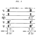
- input signals IN1 and IN2 can have the same wavelength or may have different wavelengths. If die wavelengths and polarizations are the same, then to avoid interfering with each other they must be sent at different times as shown by 201 and 202 of FIG. 2. However, if input signals IN1 and IN2 have different wavelengths, then they can both be inputted simultaneously and they won't interfere with each other. This is shown in FIG. 3, which will be described in detail in a later paragraph.
- control signal causes this time slot interchange (or optical cross connect capability) is described in the following paragraphs for the input signal IN1. (The same description also applies, in an equivalent manner, to input signal IN2).
- control signal typically, a pulse
- segment 11 the controllable propagation speed material
- Segment 11 of fiber 10 is a variable refractive-index material that is characterized by the property that the propagation speed of a beam passing through the material is a function of the energy of die beam that passes through the material. Furthermore, not only does the propagation speed change for the beam (e.g., control signal) that affects the change in propagation speed, but it also changes the propagation speed of other beams (e.g., "mark" signal) that pass through the material at the same time. The nonlinear interaction between the control signal and the "mark” signal is by means of cross-phase modulation due to the optical Kerr effect.
- the entire length of fiber 10 may be made of such a variable refractive-index material, but for the sake of generality, FIG.
- FIG. 1 is drawn with only a limited segment being made up of this material. Also for the sake of generality, it should be pointed out that the loop of fiber 10 in FIG. 1 does not necessarily have to be fiber. It can be a waveguide, or other means for directing the flow of light.
- the resulting phase relationship between the "mark” and “ref” signals is approximately ⁇ radians, meaning that the "mark” signal is about 180° out-of-phase to the "ref” signal.
- all of the energy of input signal IN1 exits at port 3 (non-reflected signal output port) rather than at port 1 (reflected signal output port). It may be noted in passing that the "ref” signal also passes through segment 11 and that its speed is also somewhat affected by the control signal.
- the control signal completely traverse the "mark" signal during its transit through segment 11 of the fiber loop 10. This is accomplished by requiring that the controllable propagation speed material of segment 11 have a dual speed characteristic, one that propagates the control signal at a different rate than the "mark" signal.
- the difference in the propagation speed may be a function of any controllable parameter of the control signal, such as wavelength, intensity or polarization. As long as the control signal completely traverses (or slips past) the "mark" signal within segment 11 the Sagnac switch operation is completely insensitive to the shape of the control signal or its precise timing.
- control signal may be one or more pulses to produce the overall energy needed.
- control signal requires at least a slip of S1 to traverse (or slip by) the "mark" signals of both input signals IN1 and IN2. That is, the differential in speed between the control signal and "mark” signal must result in the additional distance S1 being traveled by the control signal within segment 11.
- the control signal can be made to traverse individual pulses or groups or packets of input pulses.
- input signals IN1 and IN2 may, illustratively, represent an envelope of a packet of pulses (i.e., a plurality of pulses) rather than an individual pulse. This is shown in FIG. 3.
- control signal may utilize a different wavelength than the input signals or may have the same wavelength but a different polarization than the input signals.
- segment 11 may be appropriately selected to have a controllable parameter based on intensity alone, polarization alone, or on a combination of polarization and intensity parameters. The length of segment 11 must be selected together with the controllable parameter to ensure that the control signal can traverse or "slip" past the "mark” signal within the length of segment 11, even though the "mark” signal precedes the entrance of the control signal into segment 11.
- FIG. 3 there is shown the example of input signals IN1 and IN2 having different wavelengths and being inputted substantially simultaneously to the arrangement of FIG. 1.
- the input signals IN1 and IN2 comprise, respectively, three pulses and two pulses.
- a control signal 2 is shown being applied via coupler 50. As shown with reference to FIG. 1, control signal 2 travels in the same direction as the "ref" signal and in the opposite direction to the "mark" signal.
- input signals IN1 and IN2 are different wavelengths, then they can be applied and switched simultaneously by FIG. 1 producing a true optical cross connect function. No interference between the input pulse IN1 and IN2 would occur in FIG. 1, because the different wavelengths of light won't interfere with each other during combining in coupler 20.
- control signal 2 In the absence of control signal 2, input signal IN1 and IN2 become, respectively, output signals OUT1 and OUT2.
- the "ref" signal for both IN1 and IN2 are traversed by control signal 2 (e.g., within segment 11, control signal 2 travels a distance which exceeds by S2 the distance traveled by the "ref” signals). Because the input pulses IN1 and IN2 utilize different optical wavelengths, they do not interfere with each other while traveling in loop 10.
- coupler 20 is able to independently recombine the "mark” and "ref” signals of each input pulse IN1 and IN2 as though they did not arrive simultaneously thereat. Consequently, in a manner similar to that discussed in FIG.
- the input pulses IN1 exit coupler 40 as OUT2 and input pulses IN2 exit coupler 60 as OUT1.
- the circuit of FIG. 1 also performs a crossbar exchange operation on input signals IN1 and IN2 when control signal 2 is present. Hence, if either control signal 1 or control signal 2 is present, die crossbar exchange operation on input signals IN1 and IN2 results.
- control signal 1 and control signal 2 are present, and have the same overall energy, then no crossbar exchange operation results on output signals IN1 and IN2. This occurs because control signal 1 alters the speed of the "mark” signals the same amount that control signal 2 alters the speed of the "ref” signals.
- the "ref” and “mark” signals of input signal IN1 combine constructively at port 1 of coupler 20 and combine destructively at port 3 of coupler 20.
- the "ref” and “mark” signals of input signal IN2 combine constructively at port 3 and combine destructively at port 1 of coupler 20.
- input signal IN1 is coupled to OUT1 and input signal IN2 is coupled to OUT2.
- Shown in 400 of FIG. 4 is an application including a number of FIG. 1 cross-connect circuits 401-409 illustratively arranged to implement a rasterized exchange/bypass time slot interchanger.
- the time multiplexed input data stream A0-A6 is time slot interchanged or switched to become, illustratively, the output data stream A4, A3, A5, A1, A0, A6, A2.
- each of the cross-connect circuits 401, 404, 406 and 408 causes the cross-connection of the numbered inputs to different numbered outputs while the absence of a control signal (not shown) to cross-connect circuits 402, 403, 405, 407 and 409 causes the numbered inputs to connect straight through to the same numbered outputs.
- FIG. 5 Shown in FIG. 5 is a time sequential version of the interchanger 500. This version is implemented by folding the different rows and columns of circuits of FIG. 1 as described in United States patent 4,943,909 entitled “Computational Oragami” and issued to A. Huang on July 24, 1990, and incorporated herein by reference.
- one cross-connect circuit of FIG. 3 becomes the logic circuit 554, and by time sharing this cross-connect circuit 554 under control of a time division multiplexed control signal 551, it performs all the switching required by circuits 401-409 of FIG. 3.
- the time sequence of inputs (A0-A6) 552 are interchanged to the time sequence at outputs 453 under control of control signal 551.
- the delay units 555 each provide one time slot interval of delay. These delay units 555 sequentially store the last 3(or 4) time slot interval outputs that appeared on outputs 453 which are ultimately fed back as inputs 552.
- Sagnac switch 110 may be implemented using a Mach-Zehnder switch or other interferometer switch, using the Kerr effect, and arranged in an analogous manner to that disclosed herein.
Landscapes
- Physics & Mathematics (AREA)
- Nonlinear Science (AREA)
- Engineering & Computer Science (AREA)
- Power Engineering (AREA)
- General Physics & Mathematics (AREA)
- Optics & Photonics (AREA)
- Use Of Switch Circuits For Exchanges And Methods Of Control Of Multiplex Exchanges (AREA)
- Optical Modulation, Optical Deflection, Nonlinear Optics, Optical Demodulation, Optical Logic Elements (AREA)
Applications Claiming Priority (2)
| Application Number | Priority Date | Filing Date | Title |
|---|---|---|---|
| US78798991A | 1991-11-05 | 1991-11-05 | |
| US787989 | 1991-11-05 |
Publications (2)
| Publication Number | Publication Date |
|---|---|
| EP0541300A2 true EP0541300A2 (fr) | 1993-05-12 |
| EP0541300A3 EP0541300A3 (en) | 1993-09-08 |
Family
ID=25143108
Family Applications (1)
| Application Number | Title | Priority Date | Filing Date |
|---|---|---|---|
| EP19920309949 Withdrawn EP0541300A3 (en) | 1991-11-05 | 1992-10-30 | Optical crossbar exchange arrangement |
Country Status (3)
| Country | Link |
|---|---|
| US (1) | US5301008A (fr) |
| EP (1) | EP0541300A3 (fr) |
| JP (1) | JP2609790B2 (fr) |
Cited By (3)
| Publication number | Priority date | Publication date | Assignee | Title |
|---|---|---|---|---|
| EP0637182A3 (fr) * | 1993-07-30 | 1995-11-29 | At & T Corp | Noeud de communication optique à auto acheminement utilisant des portes sagnac. |
| WO1996038017A1 (fr) * | 1995-05-22 | 1996-11-28 | British Telecommunications Public Limited Company | Commutateur optique |
| WO2009106145A1 (fr) | 2008-02-29 | 2009-09-03 | Telefonaktiebolaget Lm Ericsson (Publ) | Traitement de signal optique |
Families Citing this family (11)
| Publication number | Priority date | Publication date | Assignee | Title |
|---|---|---|---|---|
| WO1996028758A1 (fr) * | 1995-03-15 | 1996-09-19 | Philips Electronics N.V. | Interrupteur optique |
| WO1996028868A2 (fr) * | 1995-03-15 | 1996-09-19 | Philips Electronics N.V. | Dispositif destine a moduler une serie d'impulsions optiques conformement a un signal de donnees |
| US5655039A (en) * | 1995-12-22 | 1997-08-05 | Corning, Inc. | Nonlinear optical loop mirror device including dispersion decreasing fiber |
| US5831731A (en) * | 1997-02-24 | 1998-11-03 | Massachusetts Institute Of Technology | Apparatus and method for comparing optical bits |
| US6393167B1 (en) * | 1998-07-31 | 2002-05-21 | Monica K. Davis | Fast, environmentally-stable fiber switches using a Sagnac interferometer |
| US6850662B1 (en) | 2000-07-31 | 2005-02-01 | Tellabs Operations, Inc. | Optical switch for reciprocal traffic |
| US6363182B2 (en) | 2000-07-31 | 2002-03-26 | James D. Mills | Optical switch for reciprocal traffic |
| US6731833B2 (en) | 2001-01-16 | 2004-05-04 | T-Rex Enterprises Corp. | Optical cross connect switch |
| US6535662B2 (en) * | 2001-03-09 | 2003-03-18 | The Trustees Of Princeton University | Toad having enhanced extinction ratio of the switching window |
| AU2003245629A1 (en) | 2002-06-19 | 2004-01-06 | Advanced Research Corporation | Optical waveguide path for a thermal-assisted magnetic recording head |
| JP4627549B2 (ja) * | 2005-12-07 | 2011-02-09 | 独立行政法人科学技術振興機構 | 光学非線形評価装置及び光スイッチング素子 |
Family Cites Families (5)
| Publication number | Priority date | Publication date | Assignee | Title |
|---|---|---|---|---|
| GB2191357B (en) * | 1986-06-07 | 1990-04-25 | Stc Plc | Optical switching |
| CA1298112C (fr) * | 1986-10-20 | 1992-03-31 | Nicholas John Doran | Dispositif optique |
| GB8728854D0 (en) * | 1987-12-10 | 1988-01-27 | British Telecomm | Optical device |
| US4995690A (en) * | 1989-04-24 | 1991-02-26 | Islam Mohammed N | Modulation instability-based fiber interferometric switch |
| US5144375A (en) * | 1990-05-10 | 1992-09-01 | At&T Bell Laboratories | Sagnac optical logic gate |
-
1992
- 1992-10-30 EP EP19920309949 patent/EP0541300A3/en not_active Withdrawn
- 1992-11-05 JP JP4319274A patent/JP2609790B2/ja not_active Expired - Fee Related
-
1993
- 1993-05-20 US US08/065,516 patent/US5301008A/en not_active Expired - Lifetime
Cited By (6)
| Publication number | Priority date | Publication date | Assignee | Title |
|---|---|---|---|---|
| EP0637182A3 (fr) * | 1993-07-30 | 1995-11-29 | At & T Corp | Noeud de communication optique à auto acheminement utilisant des portes sagnac. |
| WO1996038017A1 (fr) * | 1995-05-22 | 1996-11-28 | British Telecommunications Public Limited Company | Commutateur optique |
| US6091524A (en) * | 1995-05-22 | 2000-07-18 | British Telecommunications Public Limited Company | Optical switch |
| US6215570B1 (en) | 1995-05-22 | 2001-04-10 | British Telecommunications Public Limited Company | Optical switch |
| WO2009106145A1 (fr) | 2008-02-29 | 2009-09-03 | Telefonaktiebolaget Lm Ericsson (Publ) | Traitement de signal optique |
| EP2247980B1 (fr) * | 2008-02-29 | 2014-04-16 | Telefonaktiebolaget L M Ericsson (publ) | Traitement de signal optique |
Also Published As
| Publication number | Publication date |
|---|---|
| EP0541300A3 (en) | 1993-09-08 |
| US5301008A (en) | 1994-04-05 |
| JPH0678347A (ja) | 1994-03-18 |
| JP2609790B2 (ja) | 1997-05-14 |
Similar Documents
| Publication | Publication Date | Title |
|---|---|---|
| EP0456422B1 (fr) | Porte logique optique du type Sagnac | |
| US5301008A (en) | Optical crossbar exchange arrangement | |
| Kang et al. | Comparison of Sagnac and Mach–Zehnder ultrafast all-optical interferometric switches based on a semiconductor resonant optical nonlinearity | |
| Calabretta et al. | Optical signal processing based on self-induced polarization rotation in a semiconductor optical amplifier | |
| EP0541303B1 (fr) | Registre à décalage de circulation optique | |
| EP0593208B1 (fr) | Système de communication optique | |
| US5848205A (en) | Polarization independent non-linear optical mirror | |
| EP0723716B1 (fr) | Generateur de sequence d'impulsions optiques | |
| US4923267A (en) | Optical fiber shift register | |
| EP0545544B1 (fr) | Registre à décalage optique à rebouclage linéaire | |
| JP5944844B2 (ja) | 光信号バッファメモリ回路ならびに光信号バッファ方法 | |
| US5687260A (en) | Optical fiber switch using four gate directional coupler and control pulse | |
| JP3255208B2 (ja) | 光ゲート回路 | |
| US6542269B1 (en) | Optical device for processing an optical impulse | |
| JP6969456B2 (ja) | 光信号バッファメモリ回路並びに光信号バッファ方法 | |
| EP0987844B1 (fr) | Dispositif optique de traitement d'une impulsion optique | |
| Stegeman | All-optical switching | |
| JP5944846B2 (ja) | 光信号バッファメモリ回路 | |
| JP5944849B2 (ja) | 光信号バッファメモリ回路 | |
| Perrier et al. | Demonstration of a self-clocked optical time-slot interchanger | |
| Dorren et al. | All-optical header processing and optical buffering for optical packet switching networks | |
| French et al. | All-optical routing switch with tolerance to timing jitter at 2.5 Gb/s | |
| CA2282251A1 (fr) | Dispositif optique pour le traitement d'une impulsion optique | |
| JPH09236832A (ja) | 光制御型光スイッチ |
Legal Events
| Date | Code | Title | Description |
|---|---|---|---|
| PUAI | Public reference made under article 153(3) epc to a published international application that has entered the european phase |
Free format text: ORIGINAL CODE: 0009012 |
|
| AK | Designated contracting states |
Kind code of ref document: A2 Designated state(s): DE FR GB |
|
| PUAL | Search report despatched |
Free format text: ORIGINAL CODE: 0009013 |
|
| AK | Designated contracting states |
Kind code of ref document: A3 Designated state(s): DE FR GB |
|
| 17P | Request for examination filed |
Effective date: 19940224 |
|
| RAP3 | Party data changed (applicant data changed or rights of an application transferred) |
Owner name: AT&T CORP. |
|
| 17Q | First examination report despatched |
Effective date: 19960828 |
|
| 18W | Application withdrawn |
Withdrawal date: 19961223 |