EP0556743A1 - Vorrichtung mit Substratisolation - Google Patents
Vorrichtung mit Substratisolation Download PDFInfo
- Publication number
- EP0556743A1 EP0556743A1 EP93102239A EP93102239A EP0556743A1 EP 0556743 A1 EP0556743 A1 EP 0556743A1 EP 93102239 A EP93102239 A EP 93102239A EP 93102239 A EP93102239 A EP 93102239A EP 0556743 A1 EP0556743 A1 EP 0556743A1
- Authority
- EP
- European Patent Office
- Prior art keywords
- terminal
- transistor
- substrate
- power supply
- gate
- Prior art date
- Legal status (The legal status is an assumption and is not a legal conclusion. Google has not performed a legal analysis and makes no representation as to the accuracy of the status listed.)
- Granted
Links
- 239000000758 substrate Substances 0.000 title claims abstract description 46
- 238000009413 insulation Methods 0.000 title claims abstract description 10
- 230000003071 parasitic effect Effects 0.000 claims description 18
- 239000003990 capacitor Substances 0.000 description 5
- 238000005192 partition Methods 0.000 description 5
- 238000010586 diagram Methods 0.000 description 4
- 230000006872 improvement Effects 0.000 description 3
- 230000010354 integration Effects 0.000 description 3
- 230000000670 limiting effect Effects 0.000 description 3
- 238000004519 manufacturing process Methods 0.000 description 3
- 239000000463 material Substances 0.000 description 3
- 230000004048 modification Effects 0.000 description 3
- 238000012986 modification Methods 0.000 description 3
- 230000009467 reduction Effects 0.000 description 3
- 230000004075 alteration Effects 0.000 description 2
- 230000015556 catabolic process Effects 0.000 description 2
- 238000009792 diffusion process Methods 0.000 description 2
- 239000012535 impurity Substances 0.000 description 2
- 239000012212 insulator Substances 0.000 description 2
- 230000011664 signaling Effects 0.000 description 2
- 238000010521 absorption reaction Methods 0.000 description 1
- 230000002860 competitive effect Effects 0.000 description 1
- 230000008878 coupling Effects 0.000 description 1
- 238000010168 coupling process Methods 0.000 description 1
- 238000005859 coupling reaction Methods 0.000 description 1
- 230000007423 decrease Effects 0.000 description 1
- 230000009977 dual effect Effects 0.000 description 1
- 229910021420 polycrystalline silicon Inorganic materials 0.000 description 1
- 229920005591 polysilicon Polymers 0.000 description 1
- 238000003466 welding Methods 0.000 description 1
Images


Classifications
-
- H—ELECTRICITY
- H10—SEMICONDUCTOR DEVICES; ELECTRIC SOLID-STATE DEVICES NOT OTHERWISE PROVIDED FOR
- H10D—INORGANIC ELECTRIC SEMICONDUCTOR DEVICES
- H10D89/00—Aspects of integrated devices not covered by groups H10D84/00 - H10D88/00
- H10D89/60—Integrated devices comprising arrangements for electrical or thermal protection, e.g. protection circuits against electrostatic discharge [ESD]
- H10D89/601—Integrated devices comprising arrangements for electrical or thermal protection, e.g. protection circuits against electrostatic discharge [ESD] for devices having insulated gate electrodes, e.g. for IGFETs or IGBTs
Definitions
- the present invention relates to a substrate insulation device.
- the substrate on which active and passive elements with possibly mutually different characteristics are produced.
- the elements are separated by partitions made of a material which is similar to the electrically and physically connected insulating substrate.
- the substrate of every integrated circuit is placed at the negative voltage which has the highest absolute value. In this manner, the partitions act as insulators among the various active and passive elements of the integrated circuit, allowing operation of the various elements.
- the aim of the present invention is to eliminate or substantially reduce the problems described above by providing a substrate insulation device which solves the problem of the presence of negative voltages whose modulus is greater than the reference voltage of the substrate of the integrated circuit.
- an object of the present invention is to provide a device which can maintain the functions required by a particular application even if voltages lower than the substrate reference voltage are applied.
- Another object of the present invention is to provide a device which is highly reliable, relatively easy to manufacture and at competitive costs.
- a substrate insulation device which includes a power supply, an integrated circuit substrate, and an active integrated element defined on the substrate.
- the active integrated element is connected to the power supply and includes at least one reverse-biased junction with respect to the substrate.
- the active integrated element further includes a DMOS transistor and first and second parasitic diodes.
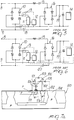
- a substrate 1 accommodates active elements 2 which are mutually insulated by means of partitions 3 made of a material which is similar to the substrate and are usually doped with impurities whose polarity is opposite to that of the impurities with which the active elements 2 are doped.
- the substrate 1 is connected to a ground 4 or to the negative voltage of a higher modulus located in an integrated circuit of any type, which is not shown.
- Junctions schematically indicated in figure 1 by the parasitic diodes 5, 6 and 7, are formed between the partitions 3 and the active portions 2 and between the substrate 1 and the active portions 2.
- the partitions 3 act as perfect insulators between the various active areas 2, with the diodes 5, 6 and 7 reverse-biased. Conversely, if negative voltages whose modulus is higher than the substrate biasing voltage are applied to the active areas 2, the diodes 5, 6 and 7 start to conduct with respect to their standard reverse-biasing condition, in which they must be in order to ensure mutual insulation among the active areas 2.
- FIG 2 which illustrates a conventional telephone circuit
- the telephone line having terminals 8 and 9
- the polarity is not set, and it is thus necessary to have, in the telephone set, a biasing bridge 10 for the talk circuit 11 and for the signalling circuit 12.
- the circuits 11 and 12, which are activated when the handset is unhooked by the closure of the switch 13, are produced in an integrated manner, and each one has its own substrate.
- the ringer circuit 14 must be DC-decoupled, i.e. no direct current must flow along the telephone line in the on-hook or ringing conditions, and a high-voltage capacitor 15 is used for this purpose.
- a full-wave rectifier 16 is used for the ringer and a discrete capacitor or filter 19 is connected in parallel with the integrated circuit 14 between the circuit 14 and rectifier 16 which supplies the integrated circuit 14 with the respective substrate.
- the insulation device includes power supplies which are connected to a terminal of an active integrated element which has, with respect to a substrate on which it is defined, at least one reverse-biased junction.
- circuits arranged above the substrate shown schematically represent the real and parasitic connections between the active integrated component and the substrate which encloses them.
- the active integrated element comprises a DMOS transistor, generally designated by the reference numeral 100, which has its source terminal 101 connected to the body (P-type diffusion) and connected to the drain terminal 102 through a first parasitic diode 103.
- the drain terminal 102 is connected to a portion 104 of the insulating substrate through a second parasitic diode 105, and the gate terminal 106 is connected to a power supply (not shown).
- Parasitic diode 103 which includes a reverse-biased junction, is connected to the drain terminal 102 by means of its cathode terminal and to the source terminal 101 by means of its anode terminal; the source terminal is connected to the body (P-type diffusion) of the DMOS transistor 100.
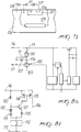
- a protection Zener diode 107 is integrated, as shown in figure 7b, in parallel to the gate terminal 106 and is connected to the substrate 104 by means of a third parasitic diode 108 and to an active area 109 by means of a fourth parasitic diode 110.
- the Zener diode 107 protects the gate terminal 106 by virtue of its own breakdown voltage, which must be lower than the maximum gate-source breakdown voltage.
- Figure 8a shows schematically the transistor and substrate 100, integral circuitry therewith, and connections to a power supply.
- an integrated resistor 111 which can be defined on the substrate 104 with highly resistive polysilicon having a resistance of 2 kohm/square mm or with a diffused resistor, technically known as a "drain extension", with a resistance of 20 kohm/square mm, using particular layout solutions.
- the DMOS transistor 100 is switched on by closing a switch 112 which connects a second resistor 113 to the gate terminal 106.
- This provides a voltage divider between the resistors 111 and 113 which limits the minimum operating voltage, while the absorption current is not constant.
- the gate terminal 106 is driven by a power supply, such as a current source which includes a first diode-connected bipolar transistor 114 and a second bipolar transistor 115.
- the first bipolar transistor 114 has its emitter terminal connected to a power supply terminal 116, and its base and collector terminals are connected together and to the base terminal of the second transistor 115.
- the second bipolar transistor 115 has its emitter terminal connected to the terminal 116 of the power supply and its collector terminal connected to the gate terminal 106 of the DMOS transistor 100.
- the current source also includes switch 112, which is connected to another terminal 117 of the power supply; a third resistor 118 and the cathode terminal of a first diode 119 are connected to the output terminal of the current source.
- a second diode 120 is arranged in series with the first diode 119, and its anode terminal is connected to a fourth resistor 122, which is connected to the terminal 116 of the power supply, and to the base terminal of a third bipolar transistor 121.
- the third transistor 121 has its emitter terminal connected to the third resistor 118 and its collector terminal connected to the collector and base terminals of the first bipolar transistor 114 and to the base terminal of the second bipolar transistor 115.
- the current source can also be realized with equivalent MOSFET transistors as will be appreciated by those skilled in the art.
- the above described current source interfaces with the gate terminal 106 through a P-type doped layer in order to eliminate any parasitic paths towards the substrate if there is a voltage which is negative with respect to the bias of the substrate.
- the voltage across the current source which interfaces with the gate terminal 106 can be practically nil, with an improvement in the minimum operating voltage.
- the device according to the invention allows integration of components providing all the functions in a single chip, i.e. on a single common substrate, with a further reduction in discrete components.
- Such integration allows a reduction in manufacturing costs in two separate ways: first, by simplifying the telephone sets' circuitry, and thus simplifying the operations for assembly and production of the printed circuit, analysis of the circuit and of the finished set; and second, in the management area, i.e. reducing storage, thereby simplifying administrative control, and the like.
- the reduction in components with the adoption of the monochip reduces constructive complexity, i.e. decreases weldings, couplings and the like.
- the materials employed, as well as the dimensions, may be any according to the requirements for the particular application.
Landscapes
- Metal-Oxide And Bipolar Metal-Oxide Semiconductor Integrated Circuits (AREA)
- Bipolar Transistors (AREA)
- Element Separation (AREA)
- Semiconductor Integrated Circuits (AREA)
Applications Claiming Priority (2)
| Application Number | Priority Date | Filing Date | Title |
|---|---|---|---|
| ITMI920338 | 1992-02-17 | ||
| ITMI920338A IT1261880B (it) | 1992-02-17 | 1992-02-17 | Dispositivo di isolamento del substrato, particolarmente per circuiti integrati |
Publications (2)
| Publication Number | Publication Date |
|---|---|
| EP0556743A1 true EP0556743A1 (de) | 1993-08-25 |
| EP0556743B1 EP0556743B1 (de) | 1999-04-28 |
Family
ID=11362007
Family Applications (1)
| Application Number | Title | Priority Date | Filing Date |
|---|---|---|---|
| EP93102239A Expired - Lifetime EP0556743B1 (de) | 1992-02-17 | 1993-02-12 | Vorrichtung mit Substratisolation |
Country Status (5)
| Country | Link |
|---|---|
| US (1) | US5525832A (de) |
| EP (1) | EP0556743B1 (de) |
| JP (1) | JPH065792A (de) |
| DE (1) | DE69324621T2 (de) |
| IT (1) | IT1261880B (de) |
Cited By (2)
| Publication number | Priority date | Publication date | Assignee | Title |
|---|---|---|---|---|
| DE10006519A1 (de) * | 2000-02-15 | 2001-08-23 | Infineon Technologies Ag | Treibertransistor |
| WO2002011199A3 (de) * | 2000-08-01 | 2002-06-27 | Infineon Technologies Ag | Nachführschaltung |
Families Citing this family (2)
| Publication number | Priority date | Publication date | Assignee | Title |
|---|---|---|---|---|
| US5925910A (en) * | 1997-03-28 | 1999-07-20 | Stmicroelectronics, Inc. | DMOS transistors with schottky diode body structure |
| EP0936674B1 (de) * | 1998-02-10 | 2006-04-26 | STMicroelectronics S.r.l. | Integrierte Schaltung mit einem VDMOS-Transistor, der gegen Überspannungen zwischen Source und Gate geschützt ist |
Family Cites Families (3)
| Publication number | Priority date | Publication date | Assignee | Title |
|---|---|---|---|---|
| US5256893A (en) * | 1987-07-22 | 1993-10-26 | Hitachi, Ltd. | Semiconductor integrated circuit device with power MOSFET incorporated |
| US5151767A (en) * | 1991-05-03 | 1992-09-29 | North American Philips Corp. | Power integrated circuit having reverse-voltage protection |
| IT1252623B (it) * | 1991-12-05 | 1995-06-19 | Sgs Thomson Microelectronics | Dispositivo a semiconduttore comprendente almeno un transistor di potenza e almeno un circuito di comando, con circuito di isolamento dinamico,integrati in maniera monolitica nella stessa piastrina |
-
1992
- 1992-02-17 IT ITMI920338A patent/IT1261880B/it active IP Right Grant
-
1993
- 1993-02-12 EP EP93102239A patent/EP0556743B1/de not_active Expired - Lifetime
- 1993-02-12 DE DE69324621T patent/DE69324621T2/de not_active Expired - Fee Related
- 1993-02-15 JP JP5025662A patent/JPH065792A/ja not_active Withdrawn
- 1993-02-16 US US08/017,816 patent/US5525832A/en not_active Expired - Lifetime
Non-Patent Citations (1)
| Title |
|---|
| IBM TECHNICAL DISCLOSURE BULLETIN vol. 29, no. 2, July 1986, NEW YORK US pages 567 - 569 'REVERSE BIAS OVER-CURRENT PROTECTION FOR POWER FIELD-EFFECT TRANSISTORS' * |
Cited By (4)
| Publication number | Priority date | Publication date | Assignee | Title |
|---|---|---|---|---|
| DE10006519A1 (de) * | 2000-02-15 | 2001-08-23 | Infineon Technologies Ag | Treibertransistor |
| DE10006519B4 (de) * | 2000-02-15 | 2004-03-11 | Infineon Technologies Ag | MOSFET-Treibertransistor und Verfahren zum Herstellen desselben |
| WO2002011199A3 (de) * | 2000-08-01 | 2002-06-27 | Infineon Technologies Ag | Nachführschaltung |
| US6800926B2 (en) | 2000-08-01 | 2004-10-05 | Infineon Technologies Ag | Tracking circuit |
Also Published As
| Publication number | Publication date |
|---|---|
| US5525832A (en) | 1996-06-11 |
| ITMI920338A1 (it) | 1993-08-17 |
| DE69324621T2 (de) | 1999-12-09 |
| DE69324621D1 (de) | 1999-06-02 |
| IT1261880B (it) | 1996-06-03 |
| ITMI920338A0 (it) | 1992-02-17 |
| EP0556743B1 (de) | 1999-04-28 |
| JPH065792A (ja) | 1994-01-14 |
Similar Documents
| Publication | Publication Date | Title |
|---|---|---|
| US5469103A (en) | Diode circuit for high speed switching transistor | |
| US7247923B2 (en) | Semiconductor device having a lateral MOSFET and combined IC using the same | |
| US4567500A (en) | Semiconductor structure for protecting integrated circuit devices | |
| US5963407A (en) | Overvoltage protection device for the protection of a power transistor having a MOS control terminal | |
| AU597540B2 (en) | Complementary lateral insulated gate rectifiers with matched "on" resistances | |
| US5274524A (en) | Programmable protection circuit and its monolithic manufacturing | |
| US4578695A (en) | Monolithic autobiased resistor structure and application thereof to interface circuits | |
| US6878996B2 (en) | MOS power transistor | |
| US6469352B2 (en) | Two-terminal semiconductor overcurrent limiter | |
| EP0512605B1 (de) | Leistungsbauelement mit Sperrspannungsschutz | |
| EP0556743B1 (de) | Vorrichtung mit Substratisolation | |
| US5172290A (en) | Gate-source protective circuit for a power mosfet | |
| US5504361A (en) | Polarity-reversal protection for integrated electronic circuits in CMOS technology | |
| US5466952A (en) | Semiconductor device having an IGET and a control or protection component | |
| JPH0282533A (ja) | バイポーラ・トランジスタ | |
| GB2141301A (en) | Protection circuit for integrated circuit devices | |
| US6787881B2 (en) | Integrated power device with improved efficiency and reduced overall dimensions | |
| US9136837B2 (en) | Switching circuit and power supply device including switch circuit | |
| KR940018964A (ko) | 반도체 장치 | |
| US6337501B1 (en) | Semiconductor device having bipolar transistor and MOS transistor | |
| US20020089018A1 (en) | Semiconductor device | |
| US4516037A (en) | Control circuitry for high voltage solid-state switches | |
| US7405913B2 (en) | Semiconductor device having transistor with high electro-static discharge capability and high noise capability | |
| JPS6348192B2 (de) | ||
| US7319263B2 (en) | Semiconductor component with switching element configured to reduce parasitic current flow |
Legal Events
| Date | Code | Title | Description |
|---|---|---|---|
| PUAI | Public reference made under article 153(3) epc to a published international application that has entered the european phase |
Free format text: ORIGINAL CODE: 0009012 |
|
| AK | Designated contracting states |
Kind code of ref document: A1 Designated state(s): DE FR GB |
|
| 17P | Request for examination filed |
Effective date: 19940221 |
|
| 17Q | First examination report despatched |
Effective date: 19960610 |
|
| GRAG | Despatch of communication of intention to grant |
Free format text: ORIGINAL CODE: EPIDOS AGRA |
|
| RAP3 | Party data changed (applicant data changed or rights of an application transferred) |
Owner name: STMICROELECTRONICS S.R.L. |
|
| GRAG | Despatch of communication of intention to grant |
Free format text: ORIGINAL CODE: EPIDOS AGRA |
|
| GRAH | Despatch of communication of intention to grant a patent |
Free format text: ORIGINAL CODE: EPIDOS IGRA |
|
| GRAH | Despatch of communication of intention to grant a patent |
Free format text: ORIGINAL CODE: EPIDOS IGRA |
|
| GRAA | (expected) grant |
Free format text: ORIGINAL CODE: 0009210 |
|
| AK | Designated contracting states |
Kind code of ref document: B1 Designated state(s): DE FR GB |
|
| REF | Corresponds to: |
Ref document number: 69324621 Country of ref document: DE Date of ref document: 19990602 |
|
| ET | Fr: translation filed | ||
| PLBE | No opposition filed within time limit |
Free format text: ORIGINAL CODE: 0009261 |
|
| STAA | Information on the status of an ep patent application or granted ep patent |
Free format text: STATUS: NO OPPOSITION FILED WITHIN TIME LIMIT |
|
| 26N | No opposition filed | ||
| REG | Reference to a national code |
Ref country code: GB Ref legal event code: IF02 |
|
| PGFP | Annual fee paid to national office [announced via postgrant information from national office to epo] |
Ref country code: DE Payment date: 20020227 Year of fee payment: 10 |
|
| PG25 | Lapsed in a contracting state [announced via postgrant information from national office to epo] |
Ref country code: DE Free format text: LAPSE BECAUSE OF NON-PAYMENT OF DUE FEES Effective date: 20030902 |
|
| PGFP | Annual fee paid to national office [announced via postgrant information from national office to epo] |
Ref country code: FR Payment date: 20040210 Year of fee payment: 12 |
|
| PGFP | Annual fee paid to national office [announced via postgrant information from national office to epo] |
Ref country code: GB Payment date: 20040211 Year of fee payment: 12 |
|
| PG25 | Lapsed in a contracting state [announced via postgrant information from national office to epo] |
Ref country code: GB Free format text: LAPSE BECAUSE OF NON-PAYMENT OF DUE FEES Effective date: 20050212 |
|
| GBPC | Gb: european patent ceased through non-payment of renewal fee |
Effective date: 20050212 |
|
| PG25 | Lapsed in a contracting state [announced via postgrant information from national office to epo] |
Ref country code: FR Free format text: LAPSE BECAUSE OF NON-PAYMENT OF DUE FEES Effective date: 20051031 |
|
| REG | Reference to a national code |
Ref country code: FR Ref legal event code: ST Effective date: 20051031 |