EP0566901A2 - Dispositifs électroniques ayant des oncles métalliques comprenant des composés cuivre-semi-conducteur - Google Patents
Dispositifs électroniques ayant des oncles métalliques comprenant des composés cuivre-semi-conducteur Download PDFInfo
- Publication number
- EP0566901A2 EP0566901A2 EP93105142A EP93105142A EP0566901A2 EP 0566901 A2 EP0566901 A2 EP 0566901A2 EP 93105142 A EP93105142 A EP 93105142A EP 93105142 A EP93105142 A EP 93105142A EP 0566901 A2 EP0566901 A2 EP 0566901A2
- Authority
- EP
- European Patent Office
- Prior art keywords
- layer
- copper
- substrate
- solder
- group
- Prior art date
- Legal status (The legal status is an assumption and is not a legal conclusion. Google has not performed a legal analysis and makes no representation as to the accuracy of the status listed.)
- Granted
Links
Images



Classifications
-
- H—ELECTRICITY
- H10—SEMICONDUCTOR DEVICES; ELECTRIC SOLID-STATE DEVICES NOT OTHERWISE PROVIDED FOR
- H10W—GENERIC PACKAGES, INTERCONNECTIONS, CONNECTORS OR OTHER CONSTRUCTIONAL DETAILS OF DEVICES COVERED BY CLASS H10
- H10W20/00—Interconnections in chips, wafers or substrates
- H10W20/40—Interconnections external to wafers or substrates, e.g. back-end-of-line [BEOL] metallisations or vias connecting to gate electrodes
- H10W20/41—Interconnections external to wafers or substrates, e.g. back-end-of-line [BEOL] metallisations or vias connecting to gate electrodes characterised by their conductive parts
- H10W20/44—Conductive materials thereof
- H10W20/4451—Semiconductor materials, e.g. polysilicon
-
- C—CHEMISTRY; METALLURGY
- C23—COATING METALLIC MATERIAL; COATING MATERIAL WITH METALLIC MATERIAL; CHEMICAL SURFACE TREATMENT; DIFFUSION TREATMENT OF METALLIC MATERIAL; COATING BY VACUUM EVAPORATION, BY SPUTTERING, BY ION IMPLANTATION OR BY CHEMICAL VAPOUR DEPOSITION, IN GENERAL; INHIBITING CORROSION OF METALLIC MATERIAL OR INCRUSTATION IN GENERAL
- C23C—COATING METALLIC MATERIAL; COATING MATERIAL WITH METALLIC MATERIAL; SURFACE TREATMENT OF METALLIC MATERIAL BY DIFFUSION INTO THE SURFACE, BY CHEMICAL CONVERSION OR SUBSTITUTION; COATING BY VACUUM EVAPORATION, BY SPUTTERING, BY ION IMPLANTATION OR BY CHEMICAL VAPOUR DEPOSITION, IN GENERAL
- C23C18/00—Chemical coating by decomposition of either liquid compounds or solutions of the coating forming compounds, without leaving reaction products of surface material in the coating; Contact plating
- C23C18/16—Chemical coating by decomposition of either liquid compounds or solutions of the coating forming compounds, without leaving reaction products of surface material in the coating; Contact plating by reduction or substitution, e.g. electroless plating
- C23C18/48—Coating with alloys
- C23C18/50—Coating with alloys with alloys based on iron, cobalt or nickel
-
- C—CHEMISTRY; METALLURGY
- C25—ELECTROLYTIC OR ELECTROPHORETIC PROCESSES; APPARATUS THEREFOR
- C25D—PROCESSES FOR THE ELECTROLYTIC OR ELECTROPHORETIC PRODUCTION OF COATINGS; ELECTROFORMING; APPARATUS THEREFOR
- C25D3/00—Electroplating: Baths therefor
- C25D3/02—Electroplating: Baths therefor from solutions
- C25D3/54—Electroplating: Baths therefor from solutions of metals not provided for in groups C25D3/04 - C25D3/50
-
- H—ELECTRICITY
- H10—SEMICONDUCTOR DEVICES; ELECTRIC SOLID-STATE DEVICES NOT OTHERWISE PROVIDED FOR
- H10P—GENERIC PROCESSES OR APPARATUS FOR THE MANUFACTURE OR TREATMENT OF DEVICES COVERED BY CLASS H10
- H10P14/00—Formation of materials, e.g. in the shape of layers or pillars
- H10P14/40—Formation of materials, e.g. in the shape of layers or pillars of conductive or resistive materials
- H10P14/46—Formation of materials, e.g. in the shape of layers or pillars of conductive or resistive materials using a liquid
-
- H—ELECTRICITY
- H10—SEMICONDUCTOR DEVICES; ELECTRIC SOLID-STATE DEVICES NOT OTHERWISE PROVIDED FOR
- H10P—GENERIC PROCESSES OR APPARATUS FOR THE MANUFACTURE OR TREATMENT OF DEVICES COVERED BY CLASS H10
- H10P14/00—Formation of materials, e.g. in the shape of layers or pillars
- H10P14/40—Formation of materials, e.g. in the shape of layers or pillars of conductive or resistive materials
- H10P14/46—Formation of materials, e.g. in the shape of layers or pillars of conductive or resistive materials using a liquid
- H10P14/47—Electrolytic deposition, i.e. electroplating; Electroless plating
-
- H—ELECTRICITY
- H10—SEMICONDUCTOR DEVICES; ELECTRIC SOLID-STATE DEVICES NOT OTHERWISE PROVIDED FOR
- H10P—GENERIC PROCESSES OR APPARATUS FOR THE MANUFACTURE OR TREATMENT OF DEVICES COVERED BY CLASS H10
- H10P72/00—Handling or holding of wafers, substrates or devices during manufacture or treatment thereof
- H10P72/70—Handling or holding of wafers, substrates or devices during manufacture or treatment thereof for supporting or gripping
- H10P72/74—Handling or holding of wafers, substrates or devices during manufacture or treatment thereof for supporting or gripping using temporarily an auxiliary support
-
- H—ELECTRICITY
- H10—SEMICONDUCTOR DEVICES; ELECTRIC SOLID-STATE DEVICES NOT OTHERWISE PROVIDED FOR
- H10W—GENERIC PACKAGES, INTERCONNECTIONS, CONNECTORS OR OTHER CONSTRUCTIONAL DETAILS OF DEVICES COVERED BY CLASS H10
- H10W20/00—Interconnections in chips, wafers or substrates
- H10W20/01—Manufacture or treatment
- H10W20/031—Manufacture or treatment of conductive parts of the interconnections
-
- H—ELECTRICITY
- H10—SEMICONDUCTOR DEVICES; ELECTRIC SOLID-STATE DEVICES NOT OTHERWISE PROVIDED FOR
- H10W—GENERIC PACKAGES, INTERCONNECTIONS, CONNECTORS OR OTHER CONSTRUCTIONAL DETAILS OF DEVICES COVERED BY CLASS H10
- H10W20/00—Interconnections in chips, wafers or substrates
- H10W20/01—Manufacture or treatment
- H10W20/031—Manufacture or treatment of conductive parts of the interconnections
- H10W20/032—Manufacture or treatment of conductive parts of the interconnections of conductive barrier, adhesion or liner layers
- H10W20/033—Manufacture or treatment of conductive parts of the interconnections of conductive barrier, adhesion or liner layers in openings in dielectrics
- H10W20/037—Manufacture or treatment of conductive parts of the interconnections of conductive barrier, adhesion or liner layers in openings in dielectrics the barrier, adhesion or liner layers being on top of a main fill metal
-
- H—ELECTRICITY
- H10—SEMICONDUCTOR DEVICES; ELECTRIC SOLID-STATE DEVICES NOT OTHERWISE PROVIDED FOR
- H10W—GENERIC PACKAGES, INTERCONNECTIONS, CONNECTORS OR OTHER CONSTRUCTIONAL DETAILS OF DEVICES COVERED BY CLASS H10
- H10W70/00—Package substrates; Interposers; Redistribution layers [RDL]
- H10W70/40—Leadframes
- H10W70/411—Chip-supporting parts, e.g. die pads
- H10W70/415—Leadframe inner leads serving as die pads
-
- H—ELECTRICITY
- H10—SEMICONDUCTOR DEVICES; ELECTRIC SOLID-STATE DEVICES NOT OTHERWISE PROVIDED FOR
- H10W—GENERIC PACKAGES, INTERCONNECTIONS, CONNECTORS OR OTHER CONSTRUCTIONAL DETAILS OF DEVICES COVERED BY CLASS H10
- H10W70/00—Package substrates; Interposers; Redistribution layers [RDL]
- H10W70/60—Insulating or insulated package substrates; Interposers; Redistribution layers
- H10W70/62—Insulating or insulated package substrates; Interposers; Redistribution layers characterised by their interconnections
- H10W70/66—Conductive materials thereof
- H10W70/662—Semiconductor materials
-
- H—ELECTRICITY
- H10—SEMICONDUCTOR DEVICES; ELECTRIC SOLID-STATE DEVICES NOT OTHERWISE PROVIDED FOR
- H10W—GENERIC PACKAGES, INTERCONNECTIONS, CONNECTORS OR OTHER CONSTRUCTIONAL DETAILS OF DEVICES COVERED BY CLASS H10
- H10W70/00—Package substrates; Interposers; Redistribution layers [RDL]
- H10W70/60—Insulating or insulated package substrates; Interposers; Redistribution layers
- H10W70/67—Insulating or insulated package substrates; Interposers; Redistribution layers characterised by their insulating layers or insulating parts
- H10W70/688—Flexible insulating substrates
-
- H—ELECTRICITY
- H10—SEMICONDUCTOR DEVICES; ELECTRIC SOLID-STATE DEVICES NOT OTHERWISE PROVIDED FOR
- H10W—GENERIC PACKAGES, INTERCONNECTIONS, CONNECTORS OR OTHER CONSTRUCTIONAL DETAILS OF DEVICES COVERED BY CLASS H10
- H10W72/00—Interconnections or connectors in packages
- H10W72/01—Manufacture or treatment
- H10W72/0198—Manufacture or treatment batch processes
-
- H—ELECTRICITY
- H10—SEMICONDUCTOR DEVICES; ELECTRIC SOLID-STATE DEVICES NOT OTHERWISE PROVIDED FOR
- H10W—GENERIC PACKAGES, INTERCONNECTIONS, CONNECTORS OR OTHER CONSTRUCTIONAL DETAILS OF DEVICES COVERED BY CLASS H10
- H10W72/00—Interconnections or connectors in packages
- H10W72/01—Manufacture or treatment
- H10W72/012—Manufacture or treatment of bump connectors, dummy bumps or thermal bumps
- H10W72/01231—Manufacture or treatment of bump connectors, dummy bumps or thermal bumps using blanket deposition
- H10W72/01238—Manufacture or treatment of bump connectors, dummy bumps or thermal bumps using blanket deposition in gaseous form, e.g. by CVD or PVD
-
- H—ELECTRICITY
- H10—SEMICONDUCTOR DEVICES; ELECTRIC SOLID-STATE DEVICES NOT OTHERWISE PROVIDED FOR
- H10W—GENERIC PACKAGES, INTERCONNECTIONS, CONNECTORS OR OTHER CONSTRUCTIONAL DETAILS OF DEVICES COVERED BY CLASS H10
- H10W72/00—Interconnections or connectors in packages
- H10W72/01—Manufacture or treatment
- H10W72/019—Manufacture or treatment of bond pads
- H10W72/01951—Changing the shapes of bond pads
- H10W72/01955—Changing the shapes of bond pads by using masks
-
- H—ELECTRICITY
- H10—SEMICONDUCTOR DEVICES; ELECTRIC SOLID-STATE DEVICES NOT OTHERWISE PROVIDED FOR
- H10W—GENERIC PACKAGES, INTERCONNECTIONS, CONNECTORS OR OTHER CONSTRUCTIONAL DETAILS OF DEVICES COVERED BY CLASS H10
- H10W72/00—Interconnections or connectors in packages
- H10W72/071—Connecting or disconnecting
- H10W72/073—Connecting or disconnecting of die-attach connectors
-
- H—ELECTRICITY
- H10—SEMICONDUCTOR DEVICES; ELECTRIC SOLID-STATE DEVICES NOT OTHERWISE PROVIDED FOR
- H10W—GENERIC PACKAGES, INTERCONNECTIONS, CONNECTORS OR OTHER CONSTRUCTIONAL DETAILS OF DEVICES COVERED BY CLASS H10
- H10W72/00—Interconnections or connectors in packages
- H10W72/071—Connecting or disconnecting
- H10W72/075—Connecting or disconnecting of bond wires
-
- H—ELECTRICITY
- H10—SEMICONDUCTOR DEVICES; ELECTRIC SOLID-STATE DEVICES NOT OTHERWISE PROVIDED FOR
- H10W—GENERIC PACKAGES, INTERCONNECTIONS, CONNECTORS OR OTHER CONSTRUCTIONAL DETAILS OF DEVICES COVERED BY CLASS H10
- H10W72/00—Interconnections or connectors in packages
- H10W72/071—Connecting or disconnecting
- H10W72/075—Connecting or disconnecting of bond wires
- H10W72/07502—Connecting or disconnecting of bond wires using an auxiliary member
- H10W72/07504—Connecting or disconnecting of bond wires using an auxiliary member the auxiliary member being temporary, e.g. a sacrificial coating
-
- H—ELECTRICITY
- H10—SEMICONDUCTOR DEVICES; ELECTRIC SOLID-STATE DEVICES NOT OTHERWISE PROVIDED FOR
- H10W—GENERIC PACKAGES, INTERCONNECTIONS, CONNECTORS OR OTHER CONSTRUCTIONAL DETAILS OF DEVICES COVERED BY CLASS H10
- H10W72/00—Interconnections or connectors in packages
- H10W72/071—Connecting or disconnecting
- H10W72/075—Connecting or disconnecting of bond wires
- H10W72/07531—Techniques
- H10W72/07532—Compression bonding, e.g. thermocompression bonding
-
- H—ELECTRICITY
- H10—SEMICONDUCTOR DEVICES; ELECTRIC SOLID-STATE DEVICES NOT OTHERWISE PROVIDED FOR
- H10W—GENERIC PACKAGES, INTERCONNECTIONS, CONNECTORS OR OTHER CONSTRUCTIONAL DETAILS OF DEVICES COVERED BY CLASS H10
- H10W72/00—Interconnections or connectors in packages
- H10W72/071—Connecting or disconnecting
- H10W72/075—Connecting or disconnecting of bond wires
- H10W72/07531—Techniques
- H10W72/07532—Compression bonding, e.g. thermocompression bonding
- H10W72/07533—Ultrasonic bonding, e.g. thermosonic bonding
-
- H—ELECTRICITY
- H10—SEMICONDUCTOR DEVICES; ELECTRIC SOLID-STATE DEVICES NOT OTHERWISE PROVIDED FOR
- H10W—GENERIC PACKAGES, INTERCONNECTIONS, CONNECTORS OR OTHER CONSTRUCTIONAL DETAILS OF DEVICES COVERED BY CLASS H10
- H10W72/00—Interconnections or connectors in packages
- H10W72/071—Connecting or disconnecting
- H10W72/075—Connecting or disconnecting of bond wires
- H10W72/07531—Techniques
- H10W72/07535—Applying EM radiation, e.g. induction heating or using a laser
-
- H—ELECTRICITY
- H10—SEMICONDUCTOR DEVICES; ELECTRIC SOLID-STATE DEVICES NOT OTHERWISE PROVIDED FOR
- H10W—GENERIC PACKAGES, INTERCONNECTIONS, CONNECTORS OR OTHER CONSTRUCTIONAL DETAILS OF DEVICES COVERED BY CLASS H10
- H10W72/00—Interconnections or connectors in packages
- H10W72/20—Bump connectors, e.g. solder bumps or copper pillars; Dummy bumps; Thermal bumps
- H10W72/241—Dispositions, e.g. layouts
- H10W72/242—Dispositions, e.g. layouts relative to the surface, e.g. recessed, protruding
-
- H—ELECTRICITY
- H10—SEMICONDUCTOR DEVICES; ELECTRIC SOLID-STATE DEVICES NOT OTHERWISE PROVIDED FOR
- H10W—GENERIC PACKAGES, INTERCONNECTIONS, CONNECTORS OR OTHER CONSTRUCTIONAL DETAILS OF DEVICES COVERED BY CLASS H10
- H10W72/00—Interconnections or connectors in packages
- H10W72/20—Bump connectors, e.g. solder bumps or copper pillars; Dummy bumps; Thermal bumps
- H10W72/251—Materials
- H10W72/252—Materials comprising solid metals or solid metalloids, e.g. PbSn, Ag or Cu
-
- H—ELECTRICITY
- H10—SEMICONDUCTOR DEVICES; ELECTRIC SOLID-STATE DEVICES NOT OTHERWISE PROVIDED FOR
- H10W—GENERIC PACKAGES, INTERCONNECTIONS, CONNECTORS OR OTHER CONSTRUCTIONAL DETAILS OF DEVICES COVERED BY CLASS H10
- H10W72/00—Interconnections or connectors in packages
- H10W72/20—Bump connectors, e.g. solder bumps or copper pillars; Dummy bumps; Thermal bumps
- H10W72/281—Auxiliary members
- H10W72/283—Reinforcing structures, e.g. bump collars
-
- H—ELECTRICITY
- H10—SEMICONDUCTOR DEVICES; ELECTRIC SOLID-STATE DEVICES NOT OTHERWISE PROVIDED FOR
- H10W—GENERIC PACKAGES, INTERCONNECTIONS, CONNECTORS OR OTHER CONSTRUCTIONAL DETAILS OF DEVICES COVERED BY CLASS H10
- H10W72/00—Interconnections or connectors in packages
- H10W72/20—Bump connectors, e.g. solder bumps or copper pillars; Dummy bumps; Thermal bumps
- H10W72/29—Bond pads specially adapted therefor
-
- H—ELECTRICITY
- H10—SEMICONDUCTOR DEVICES; ELECTRIC SOLID-STATE DEVICES NOT OTHERWISE PROVIDED FOR
- H10W—GENERIC PACKAGES, INTERCONNECTIONS, CONNECTORS OR OTHER CONSTRUCTIONAL DETAILS OF DEVICES COVERED BY CLASS H10
- H10W72/00—Interconnections or connectors in packages
- H10W72/30—Die-attach connectors
- H10W72/341—Dispositions of die-attach connectors, e.g. layouts
- H10W72/347—Dispositions of multiple die-attach connectors
- H10W72/348—Top-view layouts, e.g. mirror arrays
-
- H—ELECTRICITY
- H10—SEMICONDUCTOR DEVICES; ELECTRIC SOLID-STATE DEVICES NOT OTHERWISE PROVIDED FOR
- H10W—GENERIC PACKAGES, INTERCONNECTIONS, CONNECTORS OR OTHER CONSTRUCTIONAL DETAILS OF DEVICES COVERED BY CLASS H10
- H10W72/00—Interconnections or connectors in packages
- H10W72/30—Die-attach connectors
- H10W72/351—Materials of die-attach connectors
- H10W72/353—Materials of die-attach connectors not comprising solid metals or solid metalloids, e.g. ceramics
- H10W72/354—Materials of die-attach connectors not comprising solid metals or solid metalloids, e.g. ceramics comprising polymers
-
- H—ELECTRICITY
- H10—SEMICONDUCTOR DEVICES; ELECTRIC SOLID-STATE DEVICES NOT OTHERWISE PROVIDED FOR
- H10W—GENERIC PACKAGES, INTERCONNECTIONS, CONNECTORS OR OTHER CONSTRUCTIONAL DETAILS OF DEVICES COVERED BY CLASS H10
- H10W72/00—Interconnections or connectors in packages
- H10W72/50—Bond wires
- H10W72/531—Shapes of wire connectors
- H10W72/536—Shapes of wire connectors the connected ends being ball-shaped
-
- H—ELECTRICITY
- H10—SEMICONDUCTOR DEVICES; ELECTRIC SOLID-STATE DEVICES NOT OTHERWISE PROVIDED FOR
- H10W—GENERIC PACKAGES, INTERCONNECTIONS, CONNECTORS OR OTHER CONSTRUCTIONAL DETAILS OF DEVICES COVERED BY CLASS H10
- H10W72/00—Interconnections or connectors in packages
- H10W72/50—Bond wires
- H10W72/531—Shapes of wire connectors
- H10W72/5363—Shapes of wire connectors the connected ends being wedge-shaped
-
- H—ELECTRICITY
- H10—SEMICONDUCTOR DEVICES; ELECTRIC SOLID-STATE DEVICES NOT OTHERWISE PROVIDED FOR
- H10W—GENERIC PACKAGES, INTERCONNECTIONS, CONNECTORS OR OTHER CONSTRUCTIONAL DETAILS OF DEVICES COVERED BY CLASS H10
- H10W72/00—Interconnections or connectors in packages
- H10W72/50—Bond wires
- H10W72/551—Materials of bond wires
- H10W72/552—Materials of bond wires comprising metals or metalloids, e.g. silver
-
- H—ELECTRICITY
- H10—SEMICONDUCTOR DEVICES; ELECTRIC SOLID-STATE DEVICES NOT OTHERWISE PROVIDED FOR
- H10W—GENERIC PACKAGES, INTERCONNECTIONS, CONNECTORS OR OTHER CONSTRUCTIONAL DETAILS OF DEVICES COVERED BY CLASS H10
- H10W72/00—Interconnections or connectors in packages
- H10W72/50—Bond wires
- H10W72/551—Materials of bond wires
- H10W72/552—Materials of bond wires comprising metals or metalloids, e.g. silver
- H10W72/5522—Materials of bond wires comprising metals or metalloids, e.g. silver comprising gold [Au]
-
- H—ELECTRICITY
- H10—SEMICONDUCTOR DEVICES; ELECTRIC SOLID-STATE DEVICES NOT OTHERWISE PROVIDED FOR
- H10W—GENERIC PACKAGES, INTERCONNECTIONS, CONNECTORS OR OTHER CONSTRUCTIONAL DETAILS OF DEVICES COVERED BY CLASS H10
- H10W72/00—Interconnections or connectors in packages
- H10W72/50—Bond wires
- H10W72/551—Materials of bond wires
- H10W72/552—Materials of bond wires comprising metals or metalloids, e.g. silver
- H10W72/5524—Materials of bond wires comprising metals or metalloids, e.g. silver comprising aluminium [Al]
-
- H—ELECTRICITY
- H10—SEMICONDUCTOR DEVICES; ELECTRIC SOLID-STATE DEVICES NOT OTHERWISE PROVIDED FOR
- H10W—GENERIC PACKAGES, INTERCONNECTIONS, CONNECTORS OR OTHER CONSTRUCTIONAL DETAILS OF DEVICES COVERED BY CLASS H10
- H10W72/00—Interconnections or connectors in packages
- H10W72/50—Bond wires
- H10W72/551—Materials of bond wires
- H10W72/552—Materials of bond wires comprising metals or metalloids, e.g. silver
- H10W72/5525—Materials of bond wires comprising metals or metalloids, e.g. silver comprising copper [Cu]
-
- H—ELECTRICITY
- H10—SEMICONDUCTOR DEVICES; ELECTRIC SOLID-STATE DEVICES NOT OTHERWISE PROVIDED FOR
- H10W—GENERIC PACKAGES, INTERCONNECTIONS, CONNECTORS OR OTHER CONSTRUCTIONAL DETAILS OF DEVICES COVERED BY CLASS H10
- H10W72/00—Interconnections or connectors in packages
- H10W72/50—Bond wires
- H10W72/59—Bond pads specially adapted therefor
-
- H—ELECTRICITY
- H10—SEMICONDUCTOR DEVICES; ELECTRIC SOLID-STATE DEVICES NOT OTHERWISE PROVIDED FOR
- H10W—GENERIC PACKAGES, INTERCONNECTIONS, CONNECTORS OR OTHER CONSTRUCTIONAL DETAILS OF DEVICES COVERED BY CLASS H10
- H10W72/00—Interconnections or connectors in packages
- H10W72/851—Dispositions of multiple connectors or interconnections
- H10W72/853—On the same surface
- H10W72/865—Die-attach connectors and bond wires
-
- H—ELECTRICITY
- H10—SEMICONDUCTOR DEVICES; ELECTRIC SOLID-STATE DEVICES NOT OTHERWISE PROVIDED FOR
- H10W—GENERIC PACKAGES, INTERCONNECTIONS, CONNECTORS OR OTHER CONSTRUCTIONAL DETAILS OF DEVICES COVERED BY CLASS H10
- H10W72/00—Interconnections or connectors in packages
- H10W72/90—Bond pads, in general
-
- H—ELECTRICITY
- H10—SEMICONDUCTOR DEVICES; ELECTRIC SOLID-STATE DEVICES NOT OTHERWISE PROVIDED FOR
- H10W—GENERIC PACKAGES, INTERCONNECTIONS, CONNECTORS OR OTHER CONSTRUCTIONAL DETAILS OF DEVICES COVERED BY CLASS H10
- H10W72/00—Interconnections or connectors in packages
- H10W72/90—Bond pads, in general
- H10W72/921—Structures or relative sizes of bond pads
- H10W72/923—Bond pads having multiple stacked layers
-
- H—ELECTRICITY
- H10—SEMICONDUCTOR DEVICES; ELECTRIC SOLID-STATE DEVICES NOT OTHERWISE PROVIDED FOR
- H10W—GENERIC PACKAGES, INTERCONNECTIONS, CONNECTORS OR OTHER CONSTRUCTIONAL DETAILS OF DEVICES COVERED BY CLASS H10
- H10W72/00—Interconnections or connectors in packages
- H10W72/90—Bond pads, in general
- H10W72/941—Dispositions of bond pads
- H10W72/9415—Dispositions of bond pads relative to the surface, e.g. recessed, protruding
-
- H—ELECTRICITY
- H10—SEMICONDUCTOR DEVICES; ELECTRIC SOLID-STATE DEVICES NOT OTHERWISE PROVIDED FOR
- H10W—GENERIC PACKAGES, INTERCONNECTIONS, CONNECTORS OR OTHER CONSTRUCTIONAL DETAILS OF DEVICES COVERED BY CLASS H10
- H10W72/00—Interconnections or connectors in packages
- H10W72/90—Bond pads, in general
- H10W72/951—Materials of bond pads
- H10W72/952—Materials of bond pads comprising metals or metalloids, e.g. PbSn, Ag or Cu
-
- H—ELECTRICITY
- H10—SEMICONDUCTOR DEVICES; ELECTRIC SOLID-STATE DEVICES NOT OTHERWISE PROVIDED FOR
- H10W—GENERIC PACKAGES, INTERCONNECTIONS, CONNECTORS OR OTHER CONSTRUCTIONAL DETAILS OF DEVICES COVERED BY CLASS H10
- H10W72/00—Interconnections or connectors in packages
- H10W72/90—Bond pads, in general
- H10W72/981—Auxiliary members, e.g. spacers
- H10W72/983—Reinforcing structures, e.g. collars
-
- H—ELECTRICITY
- H10—SEMICONDUCTOR DEVICES; ELECTRIC SOLID-STATE DEVICES NOT OTHERWISE PROVIDED FOR
- H10W—GENERIC PACKAGES, INTERCONNECTIONS, CONNECTORS OR OTHER CONSTRUCTIONAL DETAILS OF DEVICES COVERED BY CLASS H10
- H10W74/00—Encapsulations, e.g. protective coatings
-
- H—ELECTRICITY
- H10—SEMICONDUCTOR DEVICES; ELECTRIC SOLID-STATE DEVICES NOT OTHERWISE PROVIDED FOR
- H10W—GENERIC PACKAGES, INTERCONNECTIONS, CONNECTORS OR OTHER CONSTRUCTIONAL DETAILS OF DEVICES COVERED BY CLASS H10
- H10W90/00—Package configurations
- H10W90/701—Package configurations characterised by the relative positions of pads or connectors relative to package parts
- H10W90/731—Package configurations characterised by the relative positions of pads or connectors relative to package parts of die-attach connectors
- H10W90/736—Package configurations characterised by the relative positions of pads or connectors relative to package parts of die-attach connectors between a chip and a stacked lead frame, conducting package substrate or heat sink
-
- H—ELECTRICITY
- H10—SEMICONDUCTOR DEVICES; ELECTRIC SOLID-STATE DEVICES NOT OTHERWISE PROVIDED FOR
- H10W—GENERIC PACKAGES, INTERCONNECTIONS, CONNECTORS OR OTHER CONSTRUCTIONAL DETAILS OF DEVICES COVERED BY CLASS H10
- H10W90/00—Package configurations
- H10W90/701—Package configurations characterised by the relative positions of pads or connectors relative to package parts
- H10W90/751—Package configurations characterised by the relative positions of pads or connectors relative to package parts of bond wires
- H10W90/756—Package configurations characterised by the relative positions of pads or connectors relative to package parts of bond wires between a chip and a stacked lead frame, conducting package substrate or heat sink
-
- Y—GENERAL TAGGING OF NEW TECHNOLOGICAL DEVELOPMENTS; GENERAL TAGGING OF CROSS-SECTIONAL TECHNOLOGIES SPANNING OVER SEVERAL SECTIONS OF THE IPC; TECHNICAL SUBJECTS COVERED BY FORMER USPC CROSS-REFERENCE ART COLLECTIONS [XRACs] AND DIGESTS
- Y10—TECHNICAL SUBJECTS COVERED BY FORMER USPC
- Y10S—TECHNICAL SUBJECTS COVERED BY FORMER USPC CROSS-REFERENCE ART COLLECTIONS [XRACs] AND DIGESTS
- Y10S428/00—Stock material or miscellaneous articles
- Y10S428/901—Printed circuit
-
- Y—GENERAL TAGGING OF NEW TECHNOLOGICAL DEVELOPMENTS; GENERAL TAGGING OF CROSS-SECTIONAL TECHNOLOGIES SPANNING OVER SEVERAL SECTIONS OF THE IPC; TECHNICAL SUBJECTS COVERED BY FORMER USPC CROSS-REFERENCE ART COLLECTIONS [XRACs] AND DIGESTS
- Y10—TECHNICAL SUBJECTS COVERED BY FORMER USPC
- Y10T—TECHNICAL SUBJECTS COVERED BY FORMER US CLASSIFICATION
- Y10T428/00—Stock material or miscellaneous articles
- Y10T428/24—Structurally defined web or sheet [e.g., overall dimension, etc.]
- Y10T428/24802—Discontinuous or differential coating, impregnation or bond [e.g., artwork, printing, retouched photograph, etc.]
- Y10T428/24917—Discontinuous or differential coating, impregnation or bond [e.g., artwork, printing, retouched photograph, etc.] including metal layer
Definitions
- Copending European application 91103153.2 filed January 6, 1992, entitled “COPPER-SEMICONDUCTOR COMPOUNDS CAPABLE OF BEING PRODUCED AT ROOM TEMPERATURE” describes depositing Cu as a film on the surface of a single crystalline semiconductor substrate of Si or Ge, while the substrate is held at room temperature. It has been found that the materials will react by themselves over an extended period of time to form a Cu-silicide or Cu-germanide compound interface. The process may be used to produce interconnection metallization for integrated circuits, but, in the context of existing VLSI processes, heat is used to accelerate the formation using the minimum desirable parameters of a temperature of about 150°C for about 20 minutes.
- the resulting interface junction has been found to demonstrate superior (near ideal) current/voltage characteristics and can be used as a high temperature (600-800°C) stability Ohmic/Schottky contact to Si or as a Cu diffusion barrier.
- Additional embodiments involve a Cu layer on a Ge layer on Si substrate, a Cu layer on a Si x G e 1 -x layer on Si substrate, and the use of an intermediate layer of a refractory metal such as W.
- Various other VLSI embodiments are also disclosed.
- the present invention relates to electronic devices wherein electrical conductors have surfaces containing silicon and germanium containing materials. More particularly, wires are wire bonded to these surfaces, and solder is fluxlessly bonded to these surfaces. More particularly, the silicon and germanium containing materials are used as an intermediate layer in a stack of metal layers and as an intermediate layer between a metal and dielectric layer. More particularly, the materials of the present invention are electrically deposited and decal transferred. Most particularly, the materials of the present invention are covalent compounds of silicon and germanium.
- the metal copper has very good electrical conductivity.
- VLSI very large scale integration
- An increase in circuit density corresponds to a decrease in conductor dimensions which leads to higher resistances and current densities which increase the signal losses and promote electromigration damage to the conductors on the electronic devices and packages.
- the problems drive the development of high conductivity metallurgies based on copper or gold. Increased circuit density requires multiple interconnection levels which requires fully planarized structures which are achieved by complicated processes.
- New materials are needed to reduce capacitive parasitics through low dielectric constants and also reduce residual stress while being susceptible to planarization. These, advanced materials and processes may have chemical incompatibilities with existing electrically conducting materials which may promote corrosion on the conductors, especially if copper is used as the electrical conductor.
- Gold is a commonly used corrosion resistant material. Electrical conductors on semiconductor chips and packaging substrates are commonly coated with gold to avoid corrosion. However, gold is an expensive material and must be replaced with other materials which have low resistivity and good corrosion resistance if a reduction in the cost of fabrication of electronic devices and substrates is to be achieved.
- lead frames which have a plurality of electrically conductive leads for electrically interconnecting semiconductor chip pads to packaging substrate pads are typically formed from copper having a gold coating.
- state of the art test probes as described in pending European Patent application 91112722.3 the teaching of which is incorporated herein by reference, describes the use of gold coated copper TAB lead frames for testing semiconductor devices.
- the Si and Ge materials of the present invention provide a substantially less costly substitute for gold.
- Gold is resistant to corrosion, gold does not form an oxide on exposure to atmospheric oxygen and gold is solder wettable.
- the Si and Ge materials of the present invention are substantially as corrosion resistant as gold, do not form a surface oxide and are solder wettable.
- gold is a commonly used surface metallization on semiconductor chip or packaging substrate contact pads to which wires are electrically connected by wire bonding and ultrasonic bonding. Quite surprisingly, it has been found that the Si and Ge materials of the present invention provide a surface as suitable as gold for wire bonding.
- gold is a commonly used surface for metallization on semiconductor chip or packaging substrate contact pads to provide a surface to which solder, in particular, lead/tin solder can be bonded.
- Gold is a solder wettable surface. Quite surprisingly, it has been found that the Si and Ge materials of the present invention are solder wettable.
- the properties of the Si and Ge containing materials of the present invention are comparable to that of gold. These materials are useful as an intermediate layer in multilayer metal structures, such as electrically conductive pads and lines in semiconductor chips and semiconductor chip packaging substrates.
- the materials of the present invention are resistant to oxidization and act as a diffusion barrier to oxygen, they are useful as intermediate barrier layers to prevent oxide formation.
- a broad aspect of the present invention is a semiconductor chip packaging structure having metallurgical structures containing silicon and germanium containing materials.
- the silicon and germanium containing materials are silicides and germanide.
- a wire bonded to a surface of the Si and Ge containing materials of the present invention In another more particular aspect of the packaging structure of the present invention, a wire bonded to a surface of the Si and Ge containing materials of the present invention.
- a solder mound is solder bonded to a surface of the silicon and germanium containing materials of the present invention.
- a lead frame selectively coated has a surface of the Si and Ge containing materials of the present invention.
- the lead frame provides electrical interconnection to a semiconductor chip.
- Another broad aspect of the present invention is the electroless deposition of germanium containing materials.
- Another broad aspect of the present invention is a method of decal transfer of the Si and Ge containing materials of the present invention.
- a layer of silicon or germanium is supported by a flexible support substrate.
- solder mounds such as, C4's
- substrates such as pads on packaging substrates
- solder wettable surface metallurgy for bonding.
- Aluminum/copper (Al/4%Cu) is a typical last wiring layer of a silicon chip or packaging substrate.
- a C4 cannot be solder joined directly to an Al/Cu surface layer.
- a solder bondable pad has a top Au layer overlying an intermediate adhesion and barrier layers.
- Cr/Cu/Au is a typical solder bondable surface metallurgical structure wherein the Cr layer is an adhesion layer and the Cu is a barrier layer to interdiffusion between the Au and metal layers below the Cr layer.
- the Cu must be thick enough to support rework cycles and the Cu can interdiffuse with the Au and dissolve in the solder.
- the entire structure is heated to the melting temperature of the solder. At these temperatures enhanced interdiffusion can occur.
- the Au is meant to keep the Cu from oxidizing and to provide a good surface for test probes and bonding.
- the Cu and Au may interdiffuse and permit the Cu which reaches the surface to oxidize. This oxidized surface will inhibit proper reflow joining of the chip C4 to the substrate contact pad.
- the oxide will also result in a high contact resistance for test probing.
- One solution to the joining to remove the surface oxide problem is to process the wafer or substrate through an additional flux step to remove the surface oxide before the chip joining operation or testing. This is costly and time consuming.
- a solution to the problem is to use the germanium or silicon containing materials of the present invention.
- Examples of these materials are the following covalent compounds Cu 3Ge, Ni 3Ge, C u 3Si, and N i 3Si.
- Figure 1 shows substrate 2, such as an electronic device, eg. a semiconductor chip or packaging substrate, having an electrical conductor 4 disposed on surface 6 of substrate 2.
- Conductor 4 can be a contact pad or conducting line both of which can typically be of an Al/Cu material.
- passivation layer 8 Surrounding conductor 4 is passivation layer 8 which leaves exposed region 10 of conductor 4.
- Passivation layer 8 can be an organic or inorganic material, e.g. a polyimide, Si O 2 or Si 3 N 4.
- a layer of the germanium or silicon containing material 12 is disposed in contact with region 10.
- the thickness of layer 12 can be from about 1,000 to about 10,000 angstroms.
- Selected deposition of patterns of the germanium or silicon containing materials of the present invention having low resistivity can be achieved utilizing the processes described herein.
- a photoresist or lift off stencil can be generated using standard semiconductor processing on a substrate or a molybdenum mask may be placed over the substrate.
- RF sputtering or ion-beam cleaning may be used to remove oxide, such as aluminum or copper oxide from the surface of the contact pads.
- vacuum deposition at room temperature of a film of germanium on the order of 800 ⁇ is followed by a film of copper with a thickness on the order of 1200 ⁇ .
- the host substrate is then heated to 100°C for one hour, allowing a solid-state reaction to form the alloy C u 3Ge.
- the substrate is then cooled to room temperature, removed from vacuum, and stripped of the photoresist stencil in acetone, or the molybdenum mask is removed if that masking technique was employed.
- the resulting ohmic contact is non-oxidizing with nominal values of resistivity in the range of 5 - 12 micro ohm-cm. Although the resistivity of this material is somewhat higher than that of pure copper, (> 2 micro ohms-cm) the copper is stable in the C u 3Ge form and will not diffuse into the silicon substrate. For thicker or thinner films the above values can be adjusted to achieve the desired thickness. Copper germanide films of thickness from about 1,000 ⁇ to 10,000 ⁇ are most preferable.
- a thin 1,000 ⁇ layer of Cr or Ti is added to the structure.
- the Cr or Ti is deposited on the pad surface after RF sputtering or ion beam cleaning and before the Ge is deposited.
- the order of deposition of the Cu and Ge can be reversed.
- a thin layer of Au be deposited on top of the alloy to provide a softer contact area for test probes.
- Figure 2 shows an alternate embodiment of the structure of Figure 1. All reference numerals common between Figure 1 and Figure 2 represent the same thing. On region 10 of pad 4, there is disposed an optional layer 14 of Cr or Ti of thickness of from about 200 ⁇ to about 2,000 ⁇ . Layer 14 is for for adhesion.
- a layer 16 of a germanium or silicon containing material according to the present invention of thickness from about 1,000 ⁇ to about 10,000 ⁇ .
- an optional layer 18 of soft material such as Au, Ag, In, Sn or Pb of thickness of from about 200 ⁇ to about 2,000 ⁇ .
- FIG 3 shows an additional embodiment of the invention which uses the germanium and silicon containing materials of the present invention for a top surface metallurgy (TSM) for substrates with Cu or Cr/Cu/Cr wiring. All numbers common between Figs. 1, 2 and 3 represent the same thing.
- Pad 4 is comprised of a bottom layer 20 of Cr, an intermediate layer 22 of Cu and a top layer 24 of Cr. In this case, if C u 3Ge is used, it could be manufactured by cleaning any copper oxide, as described above, from the surface 23 of the top-level metal 24, or by using commonly used photolithography techniques to open the top layer 24 of Cr of the Cr/Cu/Cr structure 4 to expose Cu layer 22 at opening 26.
- a layer 28 of, for example, germanium is deposited to a thickness of about 1,600 ⁇ followed by a layer 30 of copper of thickness of about 1,200 ⁇ .
- the process can then proceed as described above to form a copper germanide layer 32 from layer 28 and 30 as shown in Figure 4.
- Figure 4 additionally shows solder mound 34 bonded to copper germanide layer 32.
- the TSM layer consisting of C u 3Ge has several advantages over the conventional Cr/Cu/Au structure. Like Cr/Cu/Au it is wettable by solder. However, long exposure to the atmosphere at room temperature or above does not degrade the wettability of the C u 3Ge top layer.
- the pads coated with the germanium or silicon containing materials of the present invention will not become oxidized when the substrate goes through a chip joining process. There is no need to apply flux to the germanium or silicon containing layer or to expose it to an oven heating process to remove oxide prior to chip joining.
- the material should also service chip joining and rework processes with less dissolution of the C u 3Ge into the solder, thus avoiding the need for thick evaporation of copper.
- C4 solder mounds are disposed on an array of chip pads (typically by evaporation through a molybdenum mask).
- the chip with solder mounds thereon is disposed over a substrate having a corresponding array of pads.
- the substrate pads can have a germanium or silicon containing TSM layer to avoid oxidation of the surface of the substrate pad and to avoid using flux to solder join the C4's to the germanium or silicon containing TSM layer.
- C4 solder bonding is described in detail in U.S. Patent 3,429,040 and U.S. Patent 3,401,126, the teachings of both of which are incorporated herein by reference.
- the resistivity of C u 3Ge has been measured by depositing a blanket film of C u 3Ge on a blanket film of aluminum that had been deposited on silicon. The aluminum film was isolated by etching a 5 mm strip through it. The C u 3Ge was then deposited over the aluminum and annealed at 100°C.
- the Al film was 300 ⁇ , the C u 3Ge was 1870 ⁇ .
- the measured resistivity of the C u 3Ge was 13 micro ohm-cm.
- Al/Cu typically Al - 4 percent Cu
- Si diffusion from the contact area into the adjacent Al interconnection metallurgy can occur during post-deposition heat treatments.
- silicon is added to the Al metallurgy in an amount (1.0 to 1.5 weight percent) of Si in Al in excess of that required to satisfy the Si solubility in Al (0.5 weight percent of silicon).
- a technique to eliminate the residual silicon or silicon oxide is to RIE the contact pad surface after the Si diffusion step.
- the result of this is that often there still remains Si and Si oxides after the RIE process and that in addition an intermetallic layer composed of Si, Cu, O, C and F may be formed on the surface.
- An invention herein which solves the problem of an undesirable surface residue is a new structure for a contact metallurgy which places the germanium or silicon containing material on the top surface of the Al metallurgy. It has been found that a wire can be bonded directly to the Al/Cu conductor which has Si diffused therein and capped with a layer of the germanium and silicon containing materials diffused therein of the present invention.
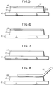
- Figures 5, 6 and 7 show steps in fabricating a structuring having a top surface of the germanium and silicon containing compounds of the present invention. All reference numerals common between Figures 5, 6 and 7 represent the same thing.
- Figure 7 allows the use of standard Al/Cu contact metallurgy as well as other metallurgy, such as Cu alone.
- a 1 micron Al/Cu layer 42 is deposited on substrate 40.
- Layer 44 of silicon is deposited on layer 42 typically by evaporation.
- a thin layer 46 of Cu is evaporated on the top surface of layer 44.
- Enough Si must be evaporated to form a layer of copper/silicon material according to the present invention and leave sufficient Si (of about 200 ⁇ ) to diffuse into the Al/Cu layer 42 to satisfy solubility requirements.
- the total is about 300 ⁇ of Si when followed by 150 ⁇ of Cu.
- the structure of Figure 5 is heat treated from about 100°C to about 300°C, preferably at 200 °C from about 10 minutes to about 60 minutes, preferably for 30 minutes to form the structure of Figure 6.
- the structure of Figure 6 is heat treated at 350°C to 450°C for 30 to 60 minutes to assure the diffusion of the Si in layer 54 into the Al/Cu layer 42 to satisfy solubility requirements.
- the processed structure consists of: approximately 1.0 micron of Al(4 percent)/Cu diffused with 0.5 percent of Si and capped by a few hundred A of a Cu/Si material according to the present invention.
- the Cu/Si material exhibits a low resistivity, on the order of about 60 micro ohm-cm, and forms a good surface for wirebonding.
- Si is typically used with Si devices and Ge is used with Ge devices.
- Figure 8 shows the structure of 7 with wire 56 bonded to surface layer 18.
- Any commonly used wire can be used, such as Al, Cu or Au wire.
- Any commonly used wire bonding technique can be used such as thermocompression bonding, ultrasonic, thermosonic bonding, laser bonding and the like.
- FIG. 9 is a schematic representation of an exploded view of a lead frame 130, a dielectric film 132 which also acts as an alpha particle barrier and a semiconductor chip 134 showing the spatial relationship of these elements for one embodiment of the present invention.
- the lead frame 130 is produced from metal sheet stock, TAB (tape automated bonding) tape, flex tape, and the like and is provided with indexing holes 36.
- the lead frame can be Cu, Cu alloy, Alloy 42 (42% Ni, 58%Fe), Invar (36% Ni, 64% Fe), Al or any other suitable electrical conductor.
- the lead frame 130 has a plurality of leads 138. Each lead 138 has an inner end 139.
- the portion of the conductors 138 which extends over the semiconductor chip 134 is separated from semiconductor chip 134 by the dielectric film 132.
- At least the interior portions 38 are coated with the germanium and silicon containing materials of the present invention to permit wire bonding thereto as described herein below.
- the dielectric film 132 is a polymeric film having a melting temperature in excess of 175°C and does not contain ionizable species such as halides and active metals including Na, K and P.
- Polyimide films can be used as the dielctric film as suggested in U.S. Pat. No. 4,426,657 by Abiru, Sugimoto and Inomata.
- One such polyimide film is Dupont Kapton®.
- the semiconductor chip 134 is attached to the lead frame conductors 138 by an adhesive layer not shown.
- a thin layer of adhesive is applied to the lead frame conductors or the top active surface 154 of chip 134.
- the top active surface 154 is one of the major surfaces of the chip 134.
- the dielectric interposer be an alpha barrier 132 positioned between the conductor and the chip.
- the adhesive layer can then be applied to both surfaces of the alpha barrier 132 with different adhesive materials used for each surface.
- the dielectric film 132 should be between about 1.5 and 2 mils thick.
- the semiconductor chip 134 is attached to the dielectric film 132 by a first adhesive layer.
- the first adhesive layer is selected from the group of epoxies, acrylics, silicones and polyimides with silicones being preferred since they minimize corrosion.
- the second adhesive layer attaches the dielectric film 132 to the conductors 138 and is selected from the group of epoxies, acrylics, silicones and polyimides.
- the second adhesive layer is selected from the group of epoxies and acrylics since these materials assure that the conductors 138 are fully bonded to the dielectric film 132, thereby enhancing the thermal conductivity between the semiconductor chip 134 and the conductors 138, and mechanically locking the lead frame conductors 138 to the semiconductor chip 134.
- Cross members 140 are provided between the conductors 138 of the lead frame 30 to impart rigidity to the lead frame 130 and to limit flow of the encapsulating material when the semiconductor chip 134, dielectric film 132, and conductor 138 are encapsulated.
- Figure 10 shows a package 142 containing a semiconductor chip 134 in which part of the encapsulating material 146 has been removes. After encapsulation, the lead frame salvage 148 and the cross members 140 shown in Figure 3 are removed. The conductors 138 which extend beyond the package 142 may be formed as required. The removed cross members are partially shown in phantom at 140' in Figure 4.
- the thickness of the conductors 138 should be minimized to ensure maximum top to bottom encapsulant sealing.
- the maximization of the encapsulant knitting at the part line 156 enhances crack resistance. Because a minimum path length of about 0.5 mm to 1 mm is needed to assure sealing of the conductors in the encapsulating material.
- Encapsulant locking of the lead frame conductors 138 is achieved by providing the conductors 138 with sharp angles or kinks 150 as shown in Figure 10.
- the package of the present invention permits the width of the semiconductor module to be reduce while maintaining superior mechanical characteristics since the length of the leads within the packaging material is no longer limited by the distance between the chip and the edge of the package.
- the conductors 138 should cover between 30% and 80% of the area of the surface of the semiconductor chip 134, and preferably a maximum percentage of the surface area.
- the conductors 138 should be positioned to avoid contact with terminal pads 152 on the semiconductor chip 134. This area maximization assures effective enhanced cooling of the semiconductor chip 134 and adequate bonding to the conductors 138 to the surface of semiconductor chip 134.
- the longer conductors 138 reaching over and adhering to the chip 134 result in a longer path (D) from the package exterior to the wire bonds thus increasing resistance to ingress of environmental contaminants which could produce corrosion and premature failure.
- Extraction of heat from the active layer 154 of the semiconductor chip 134 which contains the terminal pads 152 is more effective than extraction of heat from the back side of the semiconductor chip as is done with the packaged semiconductor chips of the prior art.
- the terminal pads 152 are connected to the conductors 138 by wires 158.
- the configuration of the conductors 138 is preferably such that wires 158 are less than about 30 mils long. Minimizing the length of the wires 158 improves the electrical performance of the packaged semiconductor chip.
- Figure 10 The structure of Figure 10 is mounted onto a substrate (not shown) and the outer ends 162 of the leads 138 are solder bonded to pads on the substrate as described herein above.
- Figure 10 shows outer ends 162 of leads 138 bent outwardly away from package 142. The outer ends may be curled inwardly under package 142, such a lead is commonly referred to as a J-lead.
- Figure 11 shows a schematic cross sectional view of a structure similar to that of Figure 10.
- Figure 11 shows lead frame 170 with wires 176 wire bonded between pads 178 on chips 180 and the inner ends 172 and 174 of leads 170.
- the chip and inner ends 172 and 174 are encapsulated in a molding compound 182 to form packaged chip structure 186.
- the outer ends 184 of lead 170 are curled inwardly towards package 186.
- the curled ends 184 can be bonded to substrate pads or contact locations 188 on substrate 190 by solder 192 as described herein above.
- the substrate 190 can be a printed circuit board, a metallized packaging ceramic substrate, flex tape and the like.
- the invention of Figures 9, 10 and 11 consists of a leadframe, copper or otherwise, which has been coated with a suitable germanium or silicon containing material such as C u 3Ge, N i 3Ge, N i 3Si and C u 3Si or other phases of these binary compounds.
- a suitable germanium or silicon containing material such as C u 3Ge, N i 3Ge, N i 3Si and C u 3Si or other phases of these binary compounds.
- the processes for forming the Si and Ge containing materials makes possible coating of any suitable lead frame material.
- the lead frame does not have to be copper.
- the coating may be applied to the location of the bonding pad (spot plating or coating) or may be used to cover the entire lead frame.
- Application of the Ge or Si containing materials may be accomplished by evaporation or by electroplating followed by heat treatment to form the material.
- C u 3Ge and N i 3Ge may also be evaporated.
- C u 3Ge may be plated by electrolytic means. It is noted that C u 3Si forms a surface oxide at temperatures above 250°C.
- Ni3Ge may be plated by electroless means.
- the unique properties of the germanium and silicon containing materials of the present invention provide an alternate bonding technique to solder bonding.
- Computer package components are generally limited by materials consideration as to the temperature to which they can be raised during an electrical or mechanical joining process.
- high-strength, high-conductivity (both electrical and thermal) connections are necessary to the art of computer packaging.
- Solder joints are commonly used for joining conductors.
- solder generally requires the application and subsequent cleaning of solder flux.
- organic epoxies may be used to join two components.
- epoxies are limited in their temperature range. Components that run hot, eg. power supplies, require a joining medium that can withstand elevated temperatures.
- a structure according to the present invention consists of two or more components that may be printed circuit boards, flexible cables, or mechanical elements that are joined mechanically, thermally, and electrically if required, by means of the medium of the germanium and silicon containing materials of the present invention, eg. C u 3Ge.
- the C u 3Ge serves as the adhesive and conductive medium.
- Each of the mechanical elements has a copper surface to which the C u 3Ge is in intimate contact in the joined structure.
- each of the surfaces of the elements to be joined is fabricated in such a way as to have a copper surface.
- Printed circuit boards and flex cables are normally fabricated in such a manner.
- the surface is not copper, then copper is applied by a suitable means: plating or evaporation, for example. Subsequently a layer of germanium, is applied to at least one of the surfaces by a suitable means: plating or evaporation for example.
- the copper surface is cleaned and brought into intimate contact with the germanium surface at a moderate temperature, typically 100 to 200 °C and under pressure, typically in the range of 10 kpsi. The result is the formation of the structure shown in Figure 12.
- a metallurgical structure 202 having at the surface 204 thereof Cu or Ni.
- Another Cu or Ni object 206 such as inner ends 139 of leads 138 of Figure 9 is adjacent surface 204 with a layer 208 of Ge or Si therebetween.
- the structure of Figure 13 is formed. Reference numerals common between Figures 12 and 13 represent the same thing.
- Layer 208 of Figure 12 becomes layer 210 which is a germanium or silicon containing compound according to the present invention.
- germanium was plated onto the contacts of a copper/polyimide flex cable.
- a mating copper printed circuit boards was first cleaned and then pressed to the cable at 20 kpsi for 60 minutes at 160°C.
- the result was a printed circuit board structure having metallurgical structure Cu/C u 3Ge/Cu/Polyimide.
- the structures were as follows: (1) Mo substrate with evaporated 200 ⁇ of chromium followed by 1.0 ⁇ m of copper; (2) 25 ⁇ m thick Upilex (other polyimide would be suitable) with evaporated layers consisting of 200 ⁇ of chromium, 1.0 ⁇ m of copper, 2,000 ⁇ of germanium. The copper surface was cleaned and pressed to the germanium surface as described above. The resulting laminated structure was: Mo/Cr/Cu/C u 3Ge/Cu/Cr/Upilex. Pull tests performed on samples of the structure yielded strengths up to 30 g/mm.
- a method for disposing Ge or Si layer 208 of Figure 12 on either member 206 or surface 204 is the decal process which is a dry process for the transfer of germanium or silicon to a conductor, such as copper or nickel.
- the decal process can be used to form a passivation layer on the copper layer.
- the decal 13 consists of a thin flexible conformal substrate 212, for example, a polymeric material, like Upilex or polyimide.
- a thin 214 layer of elemental germanium or silicon On substrate 112 there is a thin 214 layer of elemental germanium or silicon.
- Layer 214 has a thickness in the range from about 500 ⁇ to about 5,000 ⁇ , most preferably about 1,000 ⁇
- Layer 214 may be produced by evaporation, sputtering, plating after seeding, or other suitable means.
- the process consists of first cleaning the surface 216 of conductor 218. If 218 is Cu, a copper cleaning bath is used; for example sulfuric acid. Then the surface 216 is placed in contact with the germanium or silicon 214 of the decal 213. Next the two surfaces are brought into intimate contact through the application of suitable force, represented by arrow 220, by means of a press.
- a suitable press is a hydraulic press. The two pieces are held in the press at an elevated temperature from about 100 to 300°C, preferably at about 230°C, until a layer of a Ge or Si containing material, such as copper-germanium, preferably C u 3Ge, is formed on the surface 216 of the copper line 218. A time of several minutes is sufficient.
- Figure 14.1 shows the decal is pealed from the copper surface 216 as indicated by arrow 215, a Ge or Si coating 214 on the copper surface 216.
- Figure 14.2 shows the resulting structure having a Ge layer 214 disposed on a Cu surface 216.
- heat can be provided to form a Si or Ge containing material according to the present invention.
- the new structure consists of a conductor, such as Cu, capped with a layer of a germanium or silicon containing material of the present invention.
- Application may be made to any planarized or flexible copper substrate, such as thin film redistribution patterns of ceramic, silicon or other substrate.
- Printed circuit boards or portions of printed circuit boards with copper surfaces may be coated in this way, as may be flexible circuits (flex or TAB) (tape automated bonding) which use copper as a conductor.
- the decal film may be patterned before application to produce a patterned coating on a continuous copper surface.
- the coating may also be applied in a continuous manner by pressing sheets between moving rollers.
- the copper lines can be passivated on their top surface to protect them from the action of the polyamic acid used to fabricate the next layer of polyimide insulation.
- the passivation is provided as described above.
- the structure shown consists of copper conductors with polyimide insulation.
- the top surfaces of the copper lines are passivated with a silicon or germanium containing material according to the present invention.
- Figure 15 shows a structure 210 having conductors 212 and 214 embedded in dielectric body 216.
- Conductors 212 and 214 have a top layer 218 and 220 respectively of a silicon or germanium containing material of the present invention.
- Polyamic acid (PAA) layer 217 is disposed on surface 222 of dielectric body 216.
- layer 217 has openings 224 and 226 exposing layers 218 and 220 respectively.
- Layer 217 is not in contact with conductor 212 and 214 since layers 218 and 220 are therebetween, respectively.
- Layers 218 and 226 act as barrier layers to prevent Cu atoms from contacting the PAA layer 217.
- Cu atoms in contact PAA form a complex which releases Cu oxide when the PAA is heated to cure to polyimide.
- Cu oxide particles are undesirable since they increase the dielectric constant of polyimide.
- the formation of Cu oxide particles in PAA is described in U.S. Patent 5,053,272, the teaching of which is incorporated herein by reference.
- the structure 210 of Figure 15 is useful as semiconductor chip packaging substrate or the top metallization layers of such a substrate or as the top metallization layers of a semiconductor chip.
- Space 224 and 226 of Figure 15 can be filled with an electrically conductive material as shown in Figure 16 as 225 and 227.
- PAA layer 217 becomes polyimide and if body 216 is polyimide surface 222 of Figure 15 is no longer discernible. Therefore surface 222 is shown in figure 16 as a dashed line. If two polyimide layers are laminated or glued together, they remain distinct layers.
- layer 218 is an intermediate layer between conductors 212 and 225 and layer 220 is an intermediate layer between conductors 214 and 227.
- the Si and Ge materials of the present invention are useful as intermediate layers to act as interdiffusion barrier layers and corrosion inhibiting layers. This is particularly useful for conductors embedded in polymers, such as polyimide, which contain residual water which can act as an electrolyte for galvanic action between dissimilar metals. Galvanic action can lead to corrosion in the following metallurgical structure Cr/Cu/Cr or Cr/Cu/Ti/Au.
- the new structure is Cr/C u 3Ge/Cr. The thickness's are: both Cr - 200 ⁇ , C u 3Ge - 3.5 ⁇ m.
- the new structure is Cr/C u 3Ge/Ti/Au.
- the thicknesses are: Cr - 200 ⁇ , C u 3Ge - 6 ⁇ m, Ti - 1 ⁇ m and Au - 1 ⁇ m.
- C u 3Ge there are two preferred methods of depositing a layer of the Si and Ge containing materials of the present invention, e.g., C u 3Ge as an intermediate layer.
- the depositions are all carried out using the commonly known molydbenium mask procedure.
- the first method for fabrication of a layer of C u 3Ge is to evaporate in sequence Cr, Ge, Cu, Ge, Cr using approximately 2,500 ⁇ thickness for the Ge layers and 3.0 ⁇ m for the copper layer.
- the structure is annealed in-situ for 15 to 30 min at 200 to 300°C.
- the C u 3Ge may be deposited directly using a previously manufactured source of the material.
- One deposition sequence is Cr, C u 3Ge, Cu, C u 3Ge, Cr.
- the embodiment, in which all of the Cu is replaced by C u 3Ge, may be carried out either by a direct deposition of the C u 3Ge or by depositing alternating layers of Ge and Cu followed by the annealing step.
- the lead frame as shown in Figure 9 can be fabricated to have a surface layer of a Si or Ge containing material using the electroless deposition following method which is described for deposition of C u 3Ge on Cu.
- the method is not limited to this choice of materials.
- the copper may constitute a thin layer or be the bulk material of the electrical contact.
- the bulk material of the contact may be copper or another suitable material over which copper may be plated, such as BeCu or CuNi or brass.
- the contact may be in the form of a spring, may constitute a portion of a conductor adhered to a flexible substrate, or may be a free standing electrical probe such as may be used for test applications.
- the structure described above may be manufactured. If the bulk material of the contact is not copper, then first a layer of copper, on the order of 1,200 ⁇ is plated on the surface. Then germanium on the order or 800 ⁇ , 2/3 of the plated-copper thickness, is plated by electrical means over the bulk copper or over the thin copper layer over the bulk material. We have found that it is preferably to plate surfaces of undetermined area by using a constant voltage plating apparatus rather than a constant current source as described in the literature. The structure is annealed, typically at 200°C for 30 minutes to form a layer of C u 3Ge at the surface. The plating was accomplished using the following conditions.
- the bath was 7 percent GeC l 4 in propylene glycol with a temperature of 65°C. Plating was performed under constant voltage conditions. Solid germanium was used for the anode. Electrical contacts of such as in Figure 1 were plated at 35 V for less than 5 minutes. Fine pitch test probes were plated with 35 V (drawing a current of about 1 amp) for 4 minutes.
- This structure and process may be used on all electrical contacts or probe structures that are made of copper or upon which copper may be plated.
- the major advantages over the plating of gold are cost savings, and the production of a surface that is much harder than that of gold.
- the use of lead frames as test probes are described in detail in pending European Patent Application 91112722.3 the teaching of which is incorporated herein by reference.
- a bath that may be used for electroless plating of germanium compounds onto a suitable substrate.
- nickel-germanium N i 3Ge onto copper.
- a contact to GaAs devices which consists of a layer of nickel followed by a layer of electroless nickel-germanium.
- the plating bath consists of the following: A first 500 ml aqueous bath is prepared.
- the bath contains 3 g/l of nickel sulfate heptahydrate, 9 g/l of tri-sodium citrate dihydrate, 20 g/l of sodium hypo-phosphite monohydrate.
- a second 50 ml aqueous bath is prepared.
- the bath contains 50 g/l of germanium tetra-chloride, 135 g/l of sodium citrate, 48 g/l of citric acid.
- the second bath is added to the first. At 85°C the 550 ml volume is reduced to 500 ml by evaporation. Plating is accomplished on a copper substrate by submersion in the plating bath.
- the structures described above and shown in the figures may be produced by the electroless plating in nickel-germanium onto the appropriate substrate.
- the nickel-germanium surface was tested for use in bonding applications. Wirebonds and solder contacts were readily made to the surface.
Landscapes
- Chemical & Material Sciences (AREA)
- Organic Chemistry (AREA)
- Engineering & Computer Science (AREA)
- Chemical Kinetics & Catalysis (AREA)
- Materials Engineering (AREA)
- Metallurgy (AREA)
- Mechanical Engineering (AREA)
- General Chemical & Material Sciences (AREA)
- Electrochemistry (AREA)
- Electroplating Methods And Accessories (AREA)
- Lead Frames For Integrated Circuits (AREA)
- Wire Bonding (AREA)
- Internal Circuitry In Semiconductor Integrated Circuit Devices (AREA)
- Electric Connection Of Electric Components To Printed Circuits (AREA)
- Chemically Coating (AREA)
- Chemical Treatment Of Metals (AREA)
- Other Surface Treatments For Metallic Materials (AREA)
Applications Claiming Priority (2)
| Application Number | Priority Date | Filing Date | Title |
|---|---|---|---|
| US87330792A | 1992-04-24 | 1992-04-24 | |
| US873307 | 1992-04-24 |
Publications (3)
| Publication Number | Publication Date |
|---|---|
| EP0566901A2 true EP0566901A2 (fr) | 1993-10-27 |
| EP0566901A3 EP0566901A3 (fr) | 1994-01-26 |
| EP0566901B1 EP0566901B1 (fr) | 1999-05-19 |
Family
ID=25361373
Family Applications (1)
| Application Number | Title | Priority Date | Filing Date |
|---|---|---|---|
| EP19930105142 Expired - Lifetime EP0566901B1 (fr) | 1992-04-24 | 1993-03-29 | Procédé de dépÔt d'un matériau contenant du Si ou du Ge sur une surface de Cu ou de Ni |
Country Status (12)
| Country | Link |
|---|---|
| US (1) | US5855993A (fr) |
| EP (1) | EP0566901B1 (fr) |
| JP (1) | JP2526007B2 (fr) |
| KR (1) | KR0135739B1 (fr) |
| CN (1) | CN1112729C (fr) |
| AT (1) | ATE180357T1 (fr) |
| BR (1) | BR9301497A (fr) |
| CA (1) | CA2089791C (fr) |
| DE (1) | DE69324959T2 (fr) |
| ES (1) | ES2131080T3 (fr) |
| MY (1) | MY134716A (fr) |
| TW (1) | TW217459B (fr) |
Cited By (3)
| Publication number | Priority date | Publication date | Assignee | Title |
|---|---|---|---|---|
| CN102815658A (zh) * | 2011-06-08 | 2012-12-12 | 台湾积体电路制造股份有限公司 | 半导体器件 |
| WO2026030111A1 (fr) * | 2024-07-31 | 2026-02-05 | Texas Instruments Incorporated | Isolation pour puce sur dispositif conducteur et procédé de fabrication |
| WO2026030093A1 (fr) * | 2024-07-31 | 2026-02-05 | Texas Instruments Incorporated | Puce sur dispositif conducteur et procédé de fabrication |
Families Citing this family (26)
| Publication number | Priority date | Publication date | Assignee | Title |
|---|---|---|---|---|
| DE19639438A1 (de) * | 1996-09-25 | 1998-04-02 | Siemens Ag | Halbleiterkörper mit Lotmaterialschicht |
| US6082610A (en) | 1997-06-23 | 2000-07-04 | Ford Motor Company | Method of forming interconnections on electronic modules |
| US6255217B1 (en) * | 1999-01-04 | 2001-07-03 | International Business Machines Corporation | Plasma treatment to enhance inorganic dielectric adhesion to copper |
| US6271595B1 (en) * | 1999-01-14 | 2001-08-07 | International Business Machines Corporation | Method for improving adhesion to copper |
| US6251694B1 (en) * | 1999-05-26 | 2001-06-26 | United Microelectronics Corp. | Method of testing and packaging a semiconductor chip |
| US6622907B2 (en) * | 2002-02-19 | 2003-09-23 | International Business Machines Corporation | Sacrificial seed layer process for forming C4 solder bumps |
| US6703291B1 (en) * | 2002-12-17 | 2004-03-09 | Intel Corporation | Selective NiGe wet etch for transistors with Ge body and/or Ge source/drain extensions |
| JP3674927B2 (ja) * | 2003-06-13 | 2005-07-27 | Tdk株式会社 | 電子部品の製造方法および電子部品 |
| US20060147683A1 (en) * | 2004-12-30 | 2006-07-06 | Harima Chemicals, Inc. | Flux for soldering and circuit board |
| DE102005028906A1 (de) * | 2005-06-22 | 2006-12-28 | Giesecke & Devrient Gmbh | Vorrichtung für die Prüfung von Banknoten |
| US20070117475A1 (en) * | 2005-11-23 | 2007-05-24 | Regents Of The University Of California | Prevention of Sn whisker growth for high reliability electronic devices |
| US7785982B2 (en) * | 2007-01-05 | 2010-08-31 | International Business Machines Corporation | Structures containing electrodeposited germanium and methods for their fabrication |
| US7659200B2 (en) * | 2007-01-05 | 2010-02-09 | International Business Machines Corporation | Self-constrained anisotropic germanium nanostructure from electroplating |
| US8304062B2 (en) * | 2007-07-20 | 2012-11-06 | Fry's Metals, Inc. | Electrical conductors and methods of making and using them |
| US7935408B2 (en) * | 2007-10-26 | 2011-05-03 | International Business Machines Corporation | Substrate anchor structure and method |
| JP5042894B2 (ja) * | 2008-03-19 | 2012-10-03 | 松田産業株式会社 | 電子部品およびその製造方法 |
| JP5860246B2 (ja) * | 2011-08-25 | 2016-02-16 | 京セラサーキットソリューションズ株式会社 | 配線基板 |
| US8669655B2 (en) * | 2012-08-02 | 2014-03-11 | Infineon Technologies Ag | Chip package and a method for manufacturing a chip package |
| US9988713B2 (en) | 2013-03-12 | 2018-06-05 | Arizona Board Of Regents On Behalf Of Arizona State University | Thin film devices and methods for preparing thin film devices |
| US9627344B2 (en) * | 2013-04-04 | 2017-04-18 | Rohm Co., Ltd. | Semiconductor device |
| US9147605B2 (en) * | 2013-06-14 | 2015-09-29 | Arizona Board Of Regents On Behalf Of Arizona State University | Thin film devices and low temperature process to make thin film devices |
| KR101771467B1 (ko) | 2013-10-17 | 2017-08-25 | 엘에스산전 주식회사 | 배선용 차단기의 검출기구부 간격 조절방법 |
| US9559249B2 (en) | 2014-07-22 | 2017-01-31 | Arizona Board Of Regents | Microwave-annealed indium gallium zinc oxide films and methods of making the same |
| US9627575B2 (en) | 2014-09-11 | 2017-04-18 | International Business Machines Corporation | Photodiode structures |
| JP6436531B2 (ja) * | 2015-01-30 | 2018-12-12 | 住友電工デバイス・イノベーション株式会社 | 半導体装置の製造方法 |
| US11410947B2 (en) * | 2019-12-19 | 2022-08-09 | Texas Instruments Incorporated | Brass-coated metals in flip-chip redistribution layers |
Family Cites Families (17)
| Publication number | Priority date | Publication date | Assignee | Title |
|---|---|---|---|---|
| US2555001A (en) * | 1947-02-04 | 1951-05-29 | Bell Telephone Labor Inc | Bonded article and method of bonding |
| US2916401A (en) * | 1958-02-10 | 1959-12-08 | Gen Motors Corp | Chemical reduction nickel plating bath |
| US3438798A (en) * | 1965-08-23 | 1969-04-15 | Arp Inc | Electroless plating process |
| US3496014A (en) * | 1966-07-15 | 1970-02-17 | Ibm | Method of controlling the magnetic characteristics of an electrolessly deposited magnetic film |
| US4061802A (en) * | 1966-10-24 | 1977-12-06 | Costello Francis E | Plating process and bath |
| US3498823A (en) * | 1967-07-11 | 1970-03-03 | Itt | Electroless tin plating on electroless nickel |
| US3672938A (en) * | 1969-02-20 | 1972-06-27 | Kollmorgen Corp | Novel precious metal sensitizing solutions |
| US5009965A (en) * | 1974-10-04 | 1991-04-23 | Nathan Feldstein | Colloidal compositions for electroless deposition |
| US4132832A (en) * | 1976-10-12 | 1979-01-02 | Nathan Feldstein | Method of applying dispersions for activating non-conductors for electroless plating and article |
| US4355083A (en) * | 1977-06-06 | 1982-10-19 | Nathan Feldstein | Electrolessly metallized silver coated article |
| US4600656A (en) * | 1982-09-20 | 1986-07-15 | The United States Of America As Represented By The United States Department Of Energy | Electroless metal plating of plastics |
| JPS6199372A (ja) * | 1984-10-22 | 1986-05-17 | Hitachi Ltd | 電極配線 |
| US4883772A (en) * | 1986-09-11 | 1989-11-28 | National Semiconductor Corporation | Process for making a self-aligned silicide shunt |
| JPH01255235A (ja) * | 1988-04-05 | 1989-10-12 | Nec Corp | 半導体装置 |
| JPH04731A (ja) * | 1989-01-27 | 1992-01-06 | Nec Corp | 半導体装置及びその製造方法 |
| JPH03135017A (ja) * | 1989-10-20 | 1991-06-10 | Oki Electric Ind Co Ltd | 化合物半導体のオーミック電極形成方法 |
| DE69132842T2 (de) * | 1990-08-01 | 2002-08-01 | Ibm | Nassätzverfahren mit hoher Selektivität zwischen Cu und Cu3Ge |
-
1993
- 1993-02-18 CA CA 2089791 patent/CA2089791C/fr not_active Expired - Fee Related
- 1993-03-18 JP JP5058439A patent/JP2526007B2/ja not_active Expired - Fee Related
- 1993-03-29 ES ES93105142T patent/ES2131080T3/es not_active Expired - Lifetime
- 1993-03-29 DE DE69324959T patent/DE69324959T2/de not_active Expired - Lifetime
- 1993-03-29 EP EP19930105142 patent/EP0566901B1/fr not_active Expired - Lifetime
- 1993-03-29 AT AT93105142T patent/ATE180357T1/de not_active IP Right Cessation
- 1993-04-12 BR BR9301497A patent/BR9301497A/pt not_active Application Discontinuation
- 1993-04-21 MY MYPI9300721 patent/MY134716A/en unknown
- 1993-04-22 CN CN93104636A patent/CN1112729C/zh not_active Expired - Fee Related
- 1993-04-22 KR KR1019930006816A patent/KR0135739B1/ko not_active Expired - Fee Related
- 1993-06-25 TW TW82105077A patent/TW217459B/zh active
-
1994
- 1994-02-22 US US08/200,811 patent/US5855993A/en not_active Expired - Lifetime
Cited By (4)
| Publication number | Priority date | Publication date | Assignee | Title |
|---|---|---|---|---|
| CN102815658A (zh) * | 2011-06-08 | 2012-12-12 | 台湾积体电路制造股份有限公司 | 半导体器件 |
| CN102815658B (zh) * | 2011-06-08 | 2015-11-25 | 台湾积体电路制造股份有限公司 | 半导体器件 |
| WO2026030111A1 (fr) * | 2024-07-31 | 2026-02-05 | Texas Instruments Incorporated | Isolation pour puce sur dispositif conducteur et procédé de fabrication |
| WO2026030093A1 (fr) * | 2024-07-31 | 2026-02-05 | Texas Instruments Incorporated | Puce sur dispositif conducteur et procédé de fabrication |
Also Published As
| Publication number | Publication date |
|---|---|
| MY134716A (en) | 2007-12-31 |
| JPH0621140A (ja) | 1994-01-28 |
| CN1082770A (zh) | 1994-02-23 |
| JP2526007B2 (ja) | 1996-08-21 |
| KR0135739B1 (ko) | 1998-04-24 |
| CA2089791C (fr) | 1998-11-24 |
| TW217459B (fr) | 1993-12-11 |
| EP0566901B1 (fr) | 1999-05-19 |
| US5855993A (en) | 1999-01-05 |
| EP0566901A3 (fr) | 1994-01-26 |
| DE69324959D1 (de) | 1999-06-24 |
| ATE180357T1 (de) | 1999-06-15 |
| CA2089791A1 (fr) | 1993-10-25 |
| CN1112729C (zh) | 2003-06-25 |
| BR9301497A (pt) | 1993-10-26 |
| DE69324959T2 (de) | 1999-12-02 |
| ES2131080T3 (es) | 1999-07-16 |
| KR930022536A (ko) | 1993-11-24 |
Similar Documents
| Publication | Publication Date | Title |
|---|---|---|
| EP0566901B1 (fr) | Procédé de dépÔt d'un matériau contenant du Si ou du Ge sur une surface de Cu ou de Ni | |
| JP6078585B2 (ja) | 小型電子機器、その形成方法、およびシステム | |
| US3881884A (en) | Method for the formation of corrosion resistant electronic interconnections | |
| USRE46147E1 (en) | Semiconductor device and method of fabricating the same | |
| KR100213152B1 (ko) | 솔더 터미널 및 그 제조방법 | |
| US4463059A (en) | Layered metal film structures for LSI chip carriers adapted for solder bonding and wire bonding | |
| JP2001093928A (ja) | 半導体装置及びその製造方法 | |
| US6452271B2 (en) | Interconnect component for a semiconductor die including a ruthenium layer and a method for its fabrication | |
| US5540378A (en) | Method for the assembly of an electronic package | |
| CN103123916A (zh) | 半导体器件、电子器件以及半导体器件制造方法 | |
| US20240373548A1 (en) | Pre-Plating of Solder Layer on Solderable Elements for Diffusion Soldering | |
| US5633047A (en) | Electronic devices having metallurgies containing copper-semiconductor compounds | |
| KR20120122637A (ko) | 기판, 플립칩 패키지 및 그 제조방법 | |
| JP7587364B2 (ja) | 絶縁基板およびその製造方法 | |
| KR100374075B1 (ko) | 전자부품 실장용 필름캐리어 테이프 및 그 제조방법 | |
| JP3916850B2 (ja) | 半導体装置 | |
| JP2000340594A (ja) | 転写バンプシートとその製造方法 | |
| TWI288453B (en) | Tape carrier | |
| JPH0864633A (ja) | 半導体素子及び半導体装置 | |
| JP2004193211A (ja) | 電子部品およびその製造方法 | |
| JPH04335558A (ja) | 半導体装置 | |
| JPH09331015A (ja) | 半導体パッケージ及びその製造方法 | |
| JPH02292890A (ja) | 表面実装用基板 |
Legal Events
| Date | Code | Title | Description |
|---|---|---|---|
| PUAI | Public reference made under article 153(3) epc to a published international application that has entered the european phase |
Free format text: ORIGINAL CODE: 0009012 |
|
| AK | Designated contracting states |
Kind code of ref document: A2 Designated state(s): AT BE CH DE ES FR GB IT LI NL SE |
|
| PUAL | Search report despatched |
Free format text: ORIGINAL CODE: 0009013 |
|
| AK | Designated contracting states |
Kind code of ref document: A3 Designated state(s): AT BE CH DE ES FR GB IT LI NL SE |
|
| 17P | Request for examination filed |
Effective date: 19931227 |
|
| 17Q | First examination report despatched |
Effective date: 19950727 |
|
| GRAG | Despatch of communication of intention to grant |
Free format text: ORIGINAL CODE: EPIDOS AGRA |
|
| GRAG | Despatch of communication of intention to grant |
Free format text: ORIGINAL CODE: EPIDOS AGRA |
|
| GRAH | Despatch of communication of intention to grant a patent |
Free format text: ORIGINAL CODE: EPIDOS IGRA |
|
| GRAH | Despatch of communication of intention to grant a patent |
Free format text: ORIGINAL CODE: EPIDOS IGRA |
|
| GRAA | (expected) grant |
Free format text: ORIGINAL CODE: 0009210 |
|
| AK | Designated contracting states |
Kind code of ref document: B1 Designated state(s): AT BE CH DE ES FR GB IT LI NL SE |
|
| PG25 | Lapsed in a contracting state [announced via postgrant information from national office to epo] |
Ref country code: LI Free format text: LAPSE BECAUSE OF FAILURE TO SUBMIT A TRANSLATION OF THE DESCRIPTION OR TO PAY THE FEE WITHIN THE PRESCRIBED TIME-LIMIT Effective date: 19990519 Ref country code: CH Free format text: LAPSE BECAUSE OF FAILURE TO SUBMIT A TRANSLATION OF THE DESCRIPTION OR TO PAY THE FEE WITHIN THE PRESCRIBED TIME-LIMIT Effective date: 19990519 Ref country code: BE Free format text: LAPSE BECAUSE OF FAILURE TO SUBMIT A TRANSLATION OF THE DESCRIPTION OR TO PAY THE FEE WITHIN THE PRESCRIBED TIME-LIMIT Effective date: 19990519 Ref country code: AT Free format text: LAPSE BECAUSE OF FAILURE TO SUBMIT A TRANSLATION OF THE DESCRIPTION OR TO PAY THE FEE WITHIN THE PRESCRIBED TIME-LIMIT Effective date: 19990519 |
|
| REF | Corresponds to: |
Ref document number: 180357 Country of ref document: AT Date of ref document: 19990615 Kind code of ref document: T |
|
| REG | Reference to a national code |
Ref country code: CH Ref legal event code: EP |
|
| REF | Corresponds to: |
Ref document number: 69324959 Country of ref document: DE Date of ref document: 19990624 |
|
| REG | Reference to a national code |
Ref country code: ES Ref legal event code: FG2A Ref document number: 2131080 Country of ref document: ES Kind code of ref document: T3 |
|
| ET | Fr: translation filed | ||
| REG | Reference to a national code |
Ref country code: CH Ref legal event code: PL |
|
| PLBE | No opposition filed within time limit |
Free format text: ORIGINAL CODE: 0009261 |
|
| 26N | No opposition filed | ||
| PGFP | Annual fee paid to national office [announced via postgrant information from national office to epo] |
Ref country code: SE Payment date: 20010205 Year of fee payment: 9 |
|
| PGFP | Annual fee paid to national office [announced via postgrant information from national office to epo] |
Ref country code: ES Payment date: 20010308 Year of fee payment: 9 |
|
| PGFP | Annual fee paid to national office [announced via postgrant information from national office to epo] |
Ref country code: NL Payment date: 20010331 Year of fee payment: 9 |
|
| REG | Reference to a national code |
Ref country code: GB Ref legal event code: IF02 |
|
| PGFP | Annual fee paid to national office [announced via postgrant information from national office to epo] |
Ref country code: GB Payment date: 20020306 Year of fee payment: 10 |
|
| PGFP | Annual fee paid to national office [announced via postgrant information from national office to epo] |
Ref country code: FR Payment date: 20020318 Year of fee payment: 10 |
|
| PG25 | Lapsed in a contracting state [announced via postgrant information from national office to epo] |
Ref country code: SE Free format text: LAPSE BECAUSE OF NON-PAYMENT OF DUE FEES Effective date: 20020330 Ref country code: ES Free format text: LAPSE BECAUSE OF NON-PAYMENT OF DUE FEES Effective date: 20020330 |
|
| PG25 | Lapsed in a contracting state [announced via postgrant information from national office to epo] |
Ref country code: NL Free format text: LAPSE BECAUSE OF NON-PAYMENT OF DUE FEES Effective date: 20021001 |
|
| EUG | Se: european patent has lapsed |
Ref document number: 93105142.9 |
|
| NLV4 | Nl: lapsed or anulled due to non-payment of the annual fee |
Effective date: 20021001 |
|
| PG25 | Lapsed in a contracting state [announced via postgrant information from national office to epo] |
Ref country code: GB Free format text: LAPSE BECAUSE OF NON-PAYMENT OF DUE FEES Effective date: 20030329 |
|
| GBPC | Gb: european patent ceased through non-payment of renewal fee |
Effective date: 20030329 |
|
| PG25 | Lapsed in a contracting state [announced via postgrant information from national office to epo] |
Ref country code: FR Free format text: LAPSE BECAUSE OF NON-PAYMENT OF DUE FEES Effective date: 20031127 |
|
| REG | Reference to a national code |
Ref country code: FR Ref legal event code: ST |
|
| REG | Reference to a national code |
Ref country code: ES Ref legal event code: FD2A Effective date: 20030410 |
|
| PGFP | Annual fee paid to national office [announced via postgrant information from national office to epo] |
Ref country code: IT Payment date: 20060331 Year of fee payment: 14 |
|
| PG25 | Lapsed in a contracting state [announced via postgrant information from national office to epo] |
Ref country code: IT Free format text: LAPSE BECAUSE OF NON-PAYMENT OF DUE FEES Effective date: 20070329 |
|
| PGFP | Annual fee paid to national office [announced via postgrant information from national office to epo] |
Ref country code: DE Payment date: 20110328 Year of fee payment: 19 |
|
| REG | Reference to a national code |
Ref country code: DE Ref legal event code: R119 Ref document number: 69324959 Country of ref document: DE Effective date: 20121002 |
|
| PG25 | Lapsed in a contracting state [announced via postgrant information from national office to epo] |
Ref country code: DE Free format text: LAPSE BECAUSE OF NON-PAYMENT OF DUE FEES Effective date: 20121002 |
|
| REG | Reference to a national code |
Ref country code: DE Ref legal event code: R081 Ref document number: 69324959 Country of ref document: DE Owner name: GLOBALFOUNDRIES INC., KY Free format text: FORMER OWNER: INTERNATIONAL BUSINESS MACHINES CORPORATION, ARMONK, NY, US Ref country code: DE Ref legal event code: R082 Ref document number: 69324959 Country of ref document: DE Representative=s name: RICHARDT PATENTANWAELTE PARTG MBB, DE Ref country code: DE Ref legal event code: R081 Ref document number: 69324959 Country of ref document: DE Owner name: GLOBALFOUNDRIES INC., KY Free format text: FORMER OWNER: INTERNATIONAL BUSINESS MACHINES CORPORATION, ARMONK, N.Y., US |
|
| REG | Reference to a national code |
Ref country code: DE Ref legal event code: R082 Ref document number: 69324959 Country of ref document: DE Representative=s name: RICHARDT PATENTANWAELTE PARTG MBB, DE Ref country code: DE Ref legal event code: R081 Ref document number: 69324959 Country of ref document: DE Owner name: GLOBALFOUNDRIES INC., KY Free format text: FORMER OWNER: GLOBALFOUNDRIES US 2 LLC (N.D.GES.DES STAATES DELAWARE), HOPEWELL JUNCTION, N.Y., US |
|
| REG | Reference to a national code |
Ref country code: FR Ref legal event code: TP Owner name: GLOBALFOUNDRIES INC., GB Effective date: 20160829 |