EP0572704A1 - Procédé de fabrication d'un dispositif semi-conducteur comportant une méthode de réforme d'une couche isolante obtenue par CVD à basse température - Google Patents
Procédé de fabrication d'un dispositif semi-conducteur comportant une méthode de réforme d'une couche isolante obtenue par CVD à basse température Download PDFInfo
- Publication number
- EP0572704A1 EP0572704A1 EP92109549A EP92109549A EP0572704A1 EP 0572704 A1 EP0572704 A1 EP 0572704A1 EP 92109549 A EP92109549 A EP 92109549A EP 92109549 A EP92109549 A EP 92109549A EP 0572704 A1 EP0572704 A1 EP 0572704A1
- Authority
- EP
- European Patent Office
- Prior art keywords
- film
- gas
- manufacturing
- semiconductor device
- insulating film
- Prior art date
- Legal status (The legal status is an assumption and is not a legal conclusion. Google has not performed a legal analysis and makes no representation as to the accuracy of the status listed.)
- Granted
Links
Images





Classifications
-
- H—ELECTRICITY
- H10—SEMICONDUCTOR DEVICES; ELECTRIC SOLID-STATE DEVICES NOT OTHERWISE PROVIDED FOR
- H10P—GENERIC PROCESSES OR APPARATUS FOR THE MANUFACTURE OR TREATMENT OF DEVICES COVERED BY CLASS H10
- H10P14/00—Formation of materials, e.g. in the shape of layers or pillars
- H10P14/60—Formation of materials, e.g. in the shape of layers or pillars of insulating materials
- H10P14/69—Inorganic materials
- H10P14/692—Inorganic materials composed of oxides, glassy oxides or oxide-based glasses
- H10P14/6921—Inorganic materials composed of oxides, glassy oxides or oxide-based glasses containing silicon
- H10P14/69215—Inorganic materials composed of oxides, glassy oxides or oxide-based glasses containing silicon the material being a silicon oxide, e.g. SiO2
-
- H—ELECTRICITY
- H10—SEMICONDUCTOR DEVICES; ELECTRIC SOLID-STATE DEVICES NOT OTHERWISE PROVIDED FOR
- H10P—GENERIC PROCESSES OR APPARATUS FOR THE MANUFACTURE OR TREATMENT OF DEVICES COVERED BY CLASS H10
- H10P14/00—Formation of materials, e.g. in the shape of layers or pillars
- H10P14/60—Formation of materials, e.g. in the shape of layers or pillars of insulating materials
- H10P14/63—Formation of materials, e.g. in the shape of layers or pillars of insulating materials characterised by the formation processes
- H10P14/6326—Deposition processes
- H10P14/6328—Deposition from the gas or vapour phase
- H10P14/6334—Deposition from the gas or vapour phase using decomposition or reaction of gaseous or vapour phase compounds, i.e. chemical vapour deposition
- H10P14/6339—Deposition from the gas or vapour phase using decomposition or reaction of gaseous or vapour phase compounds, i.e. chemical vapour deposition deposition by cyclic CVD, e.g. ALD, ALE or pulsed CVD
-
- H—ELECTRICITY
- H10—SEMICONDUCTOR DEVICES; ELECTRIC SOLID-STATE DEVICES NOT OTHERWISE PROVIDED FOR
- H10P—GENERIC PROCESSES OR APPARATUS FOR THE MANUFACTURE OR TREATMENT OF DEVICES COVERED BY CLASS H10
- H10P14/00—Formation of materials, e.g. in the shape of layers or pillars
- H10P14/60—Formation of materials, e.g. in the shape of layers or pillars of insulating materials
- H10P14/65—Formation of materials, e.g. in the shape of layers or pillars of insulating materials characterised by treatments performed before or after the formation of the materials
- H10P14/6516—Formation of materials, e.g. in the shape of layers or pillars of insulating materials characterised by treatments performed before or after the formation of the materials of treatments performed after formation of the materials
- H10P14/6529—Formation of materials, e.g. in the shape of layers or pillars of insulating materials characterised by treatments performed before or after the formation of the materials of treatments performed after formation of the materials by exposure to a gas or vapour
- H10P14/6532—Formation of materials, e.g. in the shape of layers or pillars of insulating materials characterised by treatments performed before or after the formation of the materials of treatments performed after formation of the materials by exposure to a gas or vapour by exposure to a plasma
-
- H—ELECTRICITY
- H10—SEMICONDUCTOR DEVICES; ELECTRIC SOLID-STATE DEVICES NOT OTHERWISE PROVIDED FOR
- H10P—GENERIC PROCESSES OR APPARATUS FOR THE MANUFACTURE OR TREATMENT OF DEVICES COVERED BY CLASS H10
- H10P95/00—Generic processes or apparatus for manufacture or treatments not covered by the other groups of this subclass
-
- H—ELECTRICITY
- H10—SEMICONDUCTOR DEVICES; ELECTRIC SOLID-STATE DEVICES NOT OTHERWISE PROVIDED FOR
- H10P—GENERIC PROCESSES OR APPARATUS FOR THE MANUFACTURE OR TREATMENT OF DEVICES COVERED BY CLASS H10
- H10P14/00—Formation of materials, e.g. in the shape of layers or pillars
- H10P14/60—Formation of materials, e.g. in the shape of layers or pillars of insulating materials
- H10P14/63—Formation of materials, e.g. in the shape of layers or pillars of insulating materials characterised by the formation processes
- H10P14/6326—Deposition processes
- H10P14/6328—Deposition from the gas or vapour phase
- H10P14/6334—Deposition from the gas or vapour phase using decomposition or reaction of gaseous or vapour phase compounds, i.e. chemical vapour deposition
-
- H—ELECTRICITY
- H10—SEMICONDUCTOR DEVICES; ELECTRIC SOLID-STATE DEVICES NOT OTHERWISE PROVIDED FOR
- H10P—GENERIC PROCESSES OR APPARATUS FOR THE MANUFACTURE OR TREATMENT OF DEVICES COVERED BY CLASS H10
- H10P14/00—Formation of materials, e.g. in the shape of layers or pillars
- H10P14/60—Formation of materials, e.g. in the shape of layers or pillars of insulating materials
- H10P14/63—Formation of materials, e.g. in the shape of layers or pillars of insulating materials characterised by the formation processes
- H10P14/6326—Deposition processes
- H10P14/6328—Deposition from the gas or vapour phase
- H10P14/6334—Deposition from the gas or vapour phase using decomposition or reaction of gaseous or vapour phase compounds, i.e. chemical vapour deposition
- H10P14/6336—Deposition from the gas or vapour phase using decomposition or reaction of gaseous or vapour phase compounds, i.e. chemical vapour deposition in the presence of a plasma [PECVD]
-
- H—ELECTRICITY
- H10—SEMICONDUCTOR DEVICES; ELECTRIC SOLID-STATE DEVICES NOT OTHERWISE PROVIDED FOR
- H10P—GENERIC PROCESSES OR APPARATUS FOR THE MANUFACTURE OR TREATMENT OF DEVICES COVERED BY CLASS H10
- H10P14/00—Formation of materials, e.g. in the shape of layers or pillars
- H10P14/60—Formation of materials, e.g. in the shape of layers or pillars of insulating materials
- H10P14/69—Inorganic materials
- H10P14/692—Inorganic materials composed of oxides, glassy oxides or oxide-based glasses
- H10P14/6921—Inorganic materials composed of oxides, glassy oxides or oxide-based glasses containing silicon
- H10P14/6922—Inorganic materials composed of oxides, glassy oxides or oxide-based glasses containing silicon the material containing Si, O and at least one of H, N, C, F or other non-metal elements, e.g. SiOC, SiOC:H or SiONC
-
- H—ELECTRICITY
- H10—SEMICONDUCTOR DEVICES; ELECTRIC SOLID-STATE DEVICES NOT OTHERWISE PROVIDED FOR
- H10P—GENERIC PROCESSES OR APPARATUS FOR THE MANUFACTURE OR TREATMENT OF DEVICES COVERED BY CLASS H10
- H10P14/00—Formation of materials, e.g. in the shape of layers or pillars
- H10P14/60—Formation of materials, e.g. in the shape of layers or pillars of insulating materials
- H10P14/69—Inorganic materials
- H10P14/692—Inorganic materials composed of oxides, glassy oxides or oxide-based glasses
- H10P14/6921—Inorganic materials composed of oxides, glassy oxides or oxide-based glasses containing silicon
- H10P14/6922—Inorganic materials composed of oxides, glassy oxides or oxide-based glasses containing silicon the material containing Si, O and at least one of H, N, C, F or other non-metal elements, e.g. SiOC, SiOC:H or SiONC
- H10P14/6923—Inorganic materials composed of oxides, glassy oxides or oxide-based glasses containing silicon the material containing Si, O and at least one of H, N, C, F or other non-metal elements, e.g. SiOC, SiOC:H or SiONC the material being boron or phosphorus doped silicon oxides, e.g. BPSG, BSG or PSG
-
- Y—GENERAL TAGGING OF NEW TECHNOLOGICAL DEVELOPMENTS; GENERAL TAGGING OF CROSS-SECTIONAL TECHNOLOGIES SPANNING OVER SEVERAL SECTIONS OF THE IPC; TECHNICAL SUBJECTS COVERED BY FORMER USPC CROSS-REFERENCE ART COLLECTIONS [XRACs] AND DIGESTS
- Y10—TECHNICAL SUBJECTS COVERED BY FORMER USPC
- Y10S—TECHNICAL SUBJECTS COVERED BY FORMER USPC CROSS-REFERENCE ART COLLECTIONS [XRACs] AND DIGESTS
- Y10S148/00—Metal treatment
- Y10S148/118—Oxide films
Definitions
- the present invention relates to a method for manufacturing a semiconductor device, and more particularly to a method for manufacturing a semiconductor device including a method for reforming an insulating film formed by a low temperature CVD method.
- the object is achieved by a method for manufacturing a semiconductor device in which, after an insulating film is formed on a body to be formed by a CVD method, the temperature of the body to be formed is raised and this body is exposed to plasma gas.
- the object is achieved by a method for manufacturing a semiconductor device set forth in the first invention wherein the temperature of the body to be formed falls within the range from 350°C to 450°C while it is exposed to the plasma gas.
- the object is achieved by a method for manufacturing a semiconductor device set forth in the first invention, wherein the CVD method for forming the insulating film is performed under the condition that the reaction gas is a mixed gas of mono-silane (SiH4)/oxygen (O2) and the temperature is from 350°C to 450°C.
- the reaction gas is a mixed gas of mono-silane (SiH4)/oxygen (O2) and the temperature is from 350°C to 450°C.
- the object is achieved by a method for manufacturing a semiconductor device set forth in the first invention, wherein CVD method for forming the insulating film is performed under the condition that the reaction gas is a mixed gas of organic silane (TEOS)/ozone (O2) and the temperature is from 350°C to 450°C.
- the reaction gas is a mixed gas of organic silane (TEOS)/ozone (O2) and the temperature is from 350°C to 450°C.
- the object is achieved by a method for manufacturing a semiconductor device set forth in the first invention, wherein the insulating film formed by the CVD method is an insulating film doped with impurities.
- the object is achieved by a method for manufacturing a semiconductor device set forth in the first invention, wherein the insulating film doped with impurities is any one of a PSG film, a BSG film and a BPSG film.
- the object is achieved by a method for manufacturing a semiconductor device set forth in any one of the first thru the sixth inventions, wherein the CVD method is performed under atmospheric pressure.
- the object is achieved by a method for manufacturing a semiconductor device set forth in any one of the first thru the sixth inventions, wherein the CVD method is performed under low pressure.
- the object is achieved by a method for manufacturing a semiconductor device set forth in any one of the first thru the eighth inventions, wherein the plasma gas is inert gas, oxygen gas or ammonia gas.
- the object is achieved by a method for manufacturing a semiconductor device set forth in the first invention, wherein an insulating film is formed on the body to be formed by repeating the manufacturing method set forth in the first invention twice or more.
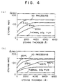
- Figs. 4(a), (b) and Figs. 5(a), (b) show the results of experiments of plasma processing performed by the present inventor using oxygen plasma gas.
- Figs. 6(a), (b), Fig. 7(c), Figs. 8(a), (b) and Figs. 9(c), (d) show the results of experiments performed by the present inventor using ammonia plasma gas.
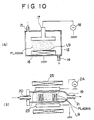
- Fig. 10(a) shows a structure of a plasma processing system used in experiments performed by the present inventor.
- a CVD SiO2 film 11 having a film thickness of 6,000 to 8,000 ⁇ is formed on a SiO2 film 10 formed by thermal oxidation on a Si substrate (wafer) 9 (Fig. 3(a)) by a CVD system as shown in Fig. 11 under such conditions that:
- a plane parallel plate type plasma processing system such as shown in Fig. 10(a)
- the wafer is heated with a heater and the wafer temperature is maintained at a constant temperature.
- an electric power having a frequency of 13.56 MHz is applied to this gas by means of an RF power supply 18 so as to activate the processing gas and to convert it into plasma, thus maintaining it for a predetermined period of time.
- Figs. 4(a) and (b) show the results of investigation on the denseness of a film by etching rate, in which Fig. 4(a) shows the result of investigating the change of the etching rate with respect to the etching thickness with plasma processing time as a parameter under the condition that the wafer temperature is maintained constant at 350°C, and Fig. 4(b) shows the result of investigating the change of the etching rate with respect to the etching thickness with the wafer temperature as a parameter under the condition that the plasma processing time is maintained constant at 5 minutes.
- Figs. 5(a) and (b) show the result of investigating the film composition by infrared absorption spectrum, wherein Fig. 5(a) shows the result of investigating existence of a bond such as Si-OH with respect to a sample processed with plasma processing time as a parameter under the condition that the wafer temperature is maintained constant at 350°C, and Fig. 5(b) shows the result of investigating existence of H2O with respect to the same sample, which show the change of absorbance to the wave number (nm ⁇ 1) with the applied electric power as a parameter. Besides, the absorbance shown along the axis of ordinates is assigned arbitrarily with respect to respective lines corresponding to respective parameters.
- H2O and the bond such as Si-OH becomes to disappear and the CVD SiO2 film 11a becomes denser as the plasma processing time gets longer or as the wafer temperature gets higher.
- This fact is considered to be caused in such a manner that H2O, Si-OH and the like are discharged outside the CVD SiO2 film 11 by that active radical particles in the plasma collide with the surface of the CVD SiO2 film 11 and the surface and the inside of the CVD SiO2 film 11 are irradiated by ultraviolet light generated by discharge.
- Fig. 6(a) shows the change of the moisture content (wt %) in a film against an applied electric power under the conditions that the wafer temperature is at 400°C and the plasma processing time is maintained constant at one minute, and also shows that the moisture content is reduced about half as compared with a sample applied with no plasma processing.
- Fig. 6(b) shows the chance of the moisture content (wt %) against the plasma processing time under the conditions that the wafer temperature is at 400°C and the applied electric power is at 200W, and also shows that the moisture content is reduced about half as compared with a sample applied with no plasma processing.
- Fig. 7(c) shows the change of the moisture content (wt %) in a film against the wafer temperature under the conditions that the applied electric power is at 200W and the plasma processing time is maintained constant at one minute, and also shows that the moisture content is reduced about half as compared with a sample applied with no plasma processing.
- Fig. 8(a) shows the result of investigating the existence of H2O with respect to the processed sample under the conditions that the plasma processing time is for one minute and the wafer temperature is maintained constant at 400°C, and shows the change of absorbance with respect to the wave number (nm ⁇ 1) with the applied electric power as a parameter.
- the absorbance shown along the axis of ordinates is assigned arbitrarily with respect to respective lines corresponding to respective parameters.
- Fig. 8(b) shows the result of investigating the existence of H2O with respect to a sample processed with the plasma processing time as a parameter under the conditions that the applied electric power is at 200W and the wafer temperature is maintained constant at 400°C. As a result, in that which has been applied with plasma processing, the peak showing the existence of H2O has disappeared irrespective of the plasma processing time.
- Fig 9(c) shows the result of investigating the existence of H2O with respect to a sample processed with the wafer temperature as a parameter under the conditions that the applied electric power is at 200W and the plasma processing time is maintained constant at one minute. As a result, the peak showing the existence of H2O becomes smaller gradually and disappears finally as the wafer temperature goes higher.
- H2O disappears by applying plasma processing, and the CVD SiO2 film 11a becomes denser. This is considered to be caused by a fact that H2O and the like are discharged outside the CVD SiO2 film 11 by that active radical particles in the plasma collide with the surface of the CVD SiO2 film 11 or the surface and the inside of the CVD SiO2 film 11 are irradiated with ultraviolet light generated by discharge.
- moisture (H2O) and the bond such as Si-OH is made to disappear so as to increase the density of the CVD SiO2 film 11a formed at a low temperature.
- moisture (H2O) and the bond such as Si-OH is made to disappear so as to increase the density of the CVD SiO2 film 11a formed at a low temperature.
- Figs. 1 (a) to (d) are sectional views for explaining a method for forming an interlevel insulating film in the first and the second embodiments of the present invention.
- Fig. 11 is a schematic diagram of a CVD system used for forming an interlevel insulating film
- Figs. 10(a) and (b) are structural diagrams of a plasma processing system used for plasma processing of an interlevel insulating film formed by the CVD system shown in Fig. 11 according to an embodiment of the present invention.
- Fig. 11 shows a CVD system for forming a SiO2 film by a thermal CVD method using mixed gas of TEOS/O3.
- a reference numeral 26 represents a chamber
- 27 represents a reaction gas inlet port for introducing reaction gas into the chamber
- 28 represents an outlet port for reducing pressure in the chamber 26 and/or exhausting processed gas and the like out of the chamber
- 30 represents a wafer placing table on which a wafer 1 as a body to be formed is placed and containing inside a heater for heating the wafer 1
- 31 represents a gas shower for having the reaction gas pour on the wafer 1.
- 32a represents a gas piping for feeding the reaction was to the chamber 26, and gas pipings 32b, 32c, 32e and 32g for feeding ozone (O3) gas, nitrogen gas containing a TEOS solution and others are connected thereto.
- 32b represents a gas piping for feeding oxygen (O2) gas or ozone gas generated by an ozonizer 33
- 32c represents a gas piping for feeding nitrogen (N2) gas containing a TEOS solution
- 32e represents a gas piping for feeding nitrogen gas containing a TMPO or TMOP (Tri Methyl Phosphate: PO (OCH3)3; hereinafter referred to as TMOP) solution
- 32g represents a gas piping for feeding nitrogen gas containing TEB (Tri Ethyl Borote) solution.
- valves 35a to 35c, 35e and 35g for regulating conduction/suspension are provided on respective gas pipings 32b, 32c, 32e and 32g.
- 32d, 32f and 32h represent gas pipings for feeding nitrogen gas to the TEOS solution, the TMOP solution and the TEB solution, respectively, and valves 35d, 35f and 35h for regulating conduction/suspension are provided on respective gas pipings 32d, 32f and 32h.
- 33 represents an ozonizer connected to the gas piping 32b
- 34a to 34c represents heaters for heating and heat insulating the TEOS solution, and TMOP solution and the TEB solution, respectively
- 36a to 36d represent mass flow controllers for regulating flow rate of oxygen gas and nitrogen gas as carrier gas.
- the TMOP solution is used for forming a PSG (phosphorous glass) film
- the TEB solution is used for forming a BSG (baron glass) film
- both of these solutions are used for forming a BPSG (boronphosphorous glass) film.
- FIG. 10(a) shows a plane parallel plate type plasma processing system.
- a reference numeral 12 in the figure represents a chamber
- 13 represents a gas inlet port for introducing processing gas into the chamber 12
- 14 represents an exhaust port for reducing pressure in the chamber 12 and/or exhausting processed gas and the like
- 16 represents a wafer placing table containing inside a heater for heating the wafer 1
- 17 represents one electrode for converting the gas into plasma. Alternating voltage is applied between this electrode 17 and the wafer placing table 16 connected to ground by means of an RF power supply 18 connected to the electrode 17 so that the processing gas introduced into the chamber 12 is converted into plasma.
- FIG. 10(b) shows another hot-wall type plasma processing system capable of batch processing.
- a reference numeral 19 in the figure represents a chamber composed of a quarts tube
- 20 represents a gas inlet port for introducing processing gas into the chamber 19
- 21 represents an exhaust port for reducing pressure in the chamber 19 and/or exhausting processed gas and the like
- 23 represents a pair of discharge electrodes for converting the processing gas into plasma. Alternating voltage is applied between one electrode and the other electrode connected to ground by means of an RF power supply 24 connected to one electrode so that the processing gas introduced into the chamber 19 is converted into plasma.
- a SiO2 film 2 is formed on a Si substrate (wafer: semiconductor substrate) 1 by the thermal oxidization, and Al interconnections 3a to 3d are formed on the SiO2 film 2 thereafter.
- valves 35a and 35b are opened so as to conduct oxygen gas into the ozonizer 33, thereby to introduce the oxygen gas into a gas piping 32 so as to obtain the ozone gas concentration in oxygen gas at approximately 1% while regulating a mass flow controller 36a.
- valves 35c and 35d are opened at the same time, and nitrogen gas of a predetermined flow rate including the TEOS solution is introduced to the gas piping 32 while regulating a mass flow controller 36b.
- the mixed gas of TEOS/O3 introduced into the gas piping 32 as described above passes through the gas inlet port 27 of the chamber 26 and is introduced into the chamber 26.
- reaction occurs on the wafer 1, and a CVD SiO2 film 4 is started to be formed.
- This state is maintained for a predetermined period of time, and Al interconnections 3a to 3c on the wafer 1 are covered so as to form the CVD SiO2 film 4 having a film thickness of approximately 8,000 ⁇ (Fig. 1(b)).
- the wafer 1 is taken out of the chamber 26 of the CVD system, and placed on the wafer placing table 16 in the chamber 12 of the plane parallel plate type plasma processing system shown in Fig. 10(a) for the purpose of reforming the CVD SiO2 film 4.
- the wafer temperature is maintained at approximately 350°C by the heater, and oxygen gas is introduced through a gas inlet port 13 while exhausting the inside of the chamber 12 through a gas exhaust port 14 and the inside of the chamber 12 is maintained at a predetermined pressure.
- high frequency voltage of the frequency at 13.56 MHz is applied between the electrode 17 and the wafer placing table 16 by the RF power supply 18 so as to convert the oxygen gas into plasma.
- the CVD SiO2 film 4 is held for 60 minutes while keeping it exposed to oxygen plasma gas, thus completing reforming of the CVD SiO2 film 4 (Figs. 1(c) and (d)).
- the CVD SiO2 film 4 is formed at a low temperature. Thus, it is possible to prevent hillocks and the like of Al interconnections 3a to 3c from being generated.
- a CVD SiO2 film 4 formed under the conditions that the mixed gas of TEOS-O3 is used at the temperature of 400°C is used in the first embodiment, but it may be formed within the range of 350°C to 450°C as the temperature condition. Further, a CVD SiO2 film formed under the conditions that the reaction gas is a mixed gas of silane (SiH4)/oxygen (O2) and the temperature is from 350°C to 450°C may also be used.
- oxygen gas is used as the gas to be converted into plasma, but it is also possible to use inert gas such as nitrogen gas and argon ga.
- a SiO2 film 2 on a Si substrate (wafer: semiconductor substrate) 1 similarly to the first embodiment Al interconnections 3a to 3c are formed on the SiO2 film 2.
- a body to be formed is constructed.
- a CVD SiO2 film (insulating film) 4 having a film thickness of approximately 8,000 ⁇ is formed on the body to be formed using the CVD system shown in Fig. 11 similarly to the first embodiment.
- the wafer 1 is taken out of the chamber 26 of the CVD system, and placed on the wafer placing table 16 in the chamber 12 of the plane parallel plate type plasma processing system shown in Fig. 10(a) for the purpose of reforming the CVD SiO2 film 4.
- the wafer 1 is heated by the heater contained inside the wafer placing table 16 so as to maintain the wafer temperature at approximately 400°C, inside of the chamber 12 is exhausted through the exhaust port 14, and ammonia gas is introduced through the gas inlet port 13 when a predetermined pressure is reached so as to maintain the pressure inside the chamber 12 at approximately 1 Torr.
- the CVD SiO2 film 4 is formed at a low temperature. Hence, it is possible to prevent hillocks and the like of Al interconnections 3a to 3c from generating.
- the wafer temperature is set at 400°C in plasma processing, but it may be set within the range of 200°C to 400°C. Further, high frequency electric power for plasma conversion is set at 200W, but the order of 100 to 300W may be adopted.
- Figs. 2(a) to (d) are sectional views for explaining a method for forming an interlevel insulating film in the third embodiment of a manufacturing method of the present invention. Plasma processing using oxygen gas is performed.
- a predetermined film thickness of 8,000 ⁇ is formed finally by applying the manufacturing method of the present invention to every film thickness of 2,000 ⁇ instead of forming the predetermined film thickness of 8,000 ⁇ at a time.
- a first CVD SiO2 film 5 having a film thickness of approximately 2,000 ⁇ is formed similarly to the first embodiment by mixed gas of TEOS/O3 using the CVD system shown in Fig. 1.
- the first CVD SiO2 film 5 is exposed to oxygen gas converted into plasma for about 30 minutes under the condition that the wafer temperature is at approximately 400°C using the plasma processing system shown in Fig. 10(a).
- the film thickness of the first CVD SiO2 film 5 is sufficiently thin as shown in Figs. 4(a), (b) and Figs. 5(a), (b) (hereinafter referred to as Fig. 4(a) and others), the film quality is improved extending over the entire film thickness.
- a second CVD SiO2 film 6 having film thickness of approximately 2,000 ⁇ is formed similarly to the process shown in Fig. 2(a), and plasma processing is applied by oxygen gas converted into plasma (Fig. 2(b)).
- the film thickness of the second CVD SiO2 film 6 is also sufficiently thin, the film quality is improved extending over the entire film thickness as shown in Fig. 4(a) and others.
- a third CVD SiO2 film 7 having a film thickness of approximately 2,000 ⁇ is formed and applied with plasma processing similarly to the above (Fig. 2(c)).
- a fourth CVD SiO2 film 8 is formed and applied with plasma processing (Fig. 2(d)).
- Fig. 2(d) plasma processing
- respective film thicknesses of the third and the fourth CVD SiO2 films 7 and 8 are also sufficiently thin, the film quality is improved extending over the entire film thickness as shown in Fig. 4(a) and others.
- a predetermined film thickness of 8,000 ⁇ is formed finally by applying the manufacturing method of the present invention to every sufficiently thin film thickness of 2,000 ⁇ . Therefore, it is possible to further improve the film quality of the CVD SiO2 films 5 to 8 as compared with the first embodiment.
- Figs. 2(a) to (d) are sectional views for explaining a method for forming an interlevel insulating film in the fourth embodiment of a manufacturing method of the present invention. Plasma processing using ammonia gas is performed therein.
- a predetermined film thickness of 8,000 ⁇ is formed finally by applying the manufacturing method of the present invention to every film thickness of 2,000 ⁇ instead of forming the predetermined film thickness of 8,000 ⁇ at a time.
- a SiO2 film 2 on a Si substrate (wafer: semiconductor substrate) 1 by thermal oxidation Al interconnections 3a to 3c are formed similarly to the second embodiment.
- a body to be formed is structured with the above.
- a first CVD SiO2 film (insulating film) 5 having a film thickness of approximately 2,000 ⁇ is formed similarly to the second embodiment by mixed gas of TEOS/O3 using the CVD system shown in Fig. 11.
- the first CVD SiO2 film 5 is exposed to ammonia gag converted into plasma for about one minute under the condition that the wafer temperature is at approximately 400°C using the plasma processing system shown in Fig. 10(a).
- the film thickness of the first CVD SiO2 film 5 is sufficiently thin, the film quality is improved extending over the entire film thickness as shown in Figs. 6(a), (b), Fig. 7(c), Figs. 8(c), (b) and Fig. 9(c) (hereinafter referred to as Fig. 6(a) and others).
- a second CVD SiO2 film (insulating film) 6 having a film thickness of approximately 2,000 ⁇ is formed similarly to the process shown in Fig. 2(a), and exposed to ammonia gas converted into plasma so as to be applied with plasma processing (Fig. 2(b)).
- the film quality is improved extending over the entire film thickness since the film thickness of the second CVD SiO2 film 6 is also sufficiently thin.
- a third CVD SiO2 film (insulating film) 7 having a film thickness of approximately 2,000 ⁇ is formed and applied with plasma processing (Fig. 2(c)) similarly to the above.
- a fourth CVD SiO2 film (insulating film) 8 is formed and applied with plasma processing (Fig. 2(d)).
- the film quality is improved extending over the entire film thickness since the film thicknesses of both the third and the fourth CVD SiO2 films 7 and 8 are sufficiently thin.
- a predetermined film thickness of 8,000 ⁇ is formed finally by applying the manufacturing method of the present invention to every sufficiently thin film thickness of 2,000 ⁇ .
- the film quality of the CVD SiO2 films 5 to 8 can be further improved as a whole as compared with the first embodiment.
Landscapes
- Formation Of Insulating Films (AREA)
Priority Applications (4)
| Application Number | Priority Date | Filing Date | Title |
|---|---|---|---|
| DE1992630934 DE69230934T2 (de) | 1992-06-05 | 1992-06-05 | Verfahren zur Herstellung einer Halbleiteranordnung mittels eines Verfahren zur Reformierung einer Isolationsschicht die bei niederiger Temperatur durch CVD hergestellt ist |
| AT92109549T ATE191991T1 (de) | 1992-06-05 | 1992-06-05 | Verfahren zur herstellung einer halbleiteranordnung mittels eines verfahren zur reformierung einer isolationsschicht die bei niederiger temperatur durch cvd hergestellt ist |
| EP92109549A EP0572704B1 (fr) | 1992-06-05 | 1992-06-05 | Procédé de fabrication d'un dispositif semi-conducteur comportant une méthode de réforme d'une couche isolante obtenue par CVD à basse température |
| US07/895,472 US5376591A (en) | 1992-06-05 | 1992-06-08 | Method for manufacturing semiconductor device |
Applications Claiming Priority (2)
| Application Number | Priority Date | Filing Date | Title |
|---|---|---|---|
| EP92109549A EP0572704B1 (fr) | 1992-06-05 | 1992-06-05 | Procédé de fabrication d'un dispositif semi-conducteur comportant une méthode de réforme d'une couche isolante obtenue par CVD à basse température |
| US07/895,472 US5376591A (en) | 1992-06-05 | 1992-06-08 | Method for manufacturing semiconductor device |
Publications (2)
| Publication Number | Publication Date |
|---|---|
| EP0572704A1 true EP0572704A1 (fr) | 1993-12-08 |
| EP0572704B1 EP0572704B1 (fr) | 2000-04-19 |
Family
ID=26130947
Family Applications (1)
| Application Number | Title | Priority Date | Filing Date |
|---|---|---|---|
| EP92109549A Expired - Lifetime EP0572704B1 (fr) | 1992-06-05 | 1992-06-05 | Procédé de fabrication d'un dispositif semi-conducteur comportant une méthode de réforme d'une couche isolante obtenue par CVD à basse température |
Country Status (2)
| Country | Link |
|---|---|
| US (1) | US5376591A (fr) |
| EP (1) | EP0572704B1 (fr) |
Cited By (4)
| Publication number | Priority date | Publication date | Assignee | Title |
|---|---|---|---|---|
| EP0653782A3 (fr) * | 1993-11-10 | 1996-04-24 | Canon Sales Co Inc | Procédé de reformage d'un film isolant. |
| EP0761841A1 (fr) * | 1995-08-18 | 1997-03-12 | Canon Sales Co., Inc. | Procédé de formation d'une couche |
| WO1999039383A1 (fr) * | 1998-01-28 | 1999-08-05 | Trikon Equipments Limited | Procede pour traiter des couches de polymere a base de silicium |
| EP1038307A4 (fr) * | 1997-12-08 | 2005-01-05 | Quester Technology Inc | Modification de surface des semiconducteurs par rayonnement electromagnetique |
Families Citing this family (27)
| Publication number | Priority date | Publication date | Assignee | Title |
|---|---|---|---|---|
| US5652187A (en) * | 1991-10-30 | 1997-07-29 | Samsung Electronics Co., Ltd. | Method for fabricating doped interlayer-dielectric film of semiconductor device using a plasma treatment |
| JP3262334B2 (ja) * | 1992-07-04 | 2002-03-04 | トリコン ホルディングズ リミテッド | 半導体ウエハーを処理する方法 |
| JPH0817173B2 (ja) * | 1993-11-10 | 1996-02-21 | キヤノン販売株式会社 | 成膜方法 |
| EP0703611B1 (fr) * | 1994-08-31 | 2007-05-02 | Texas Instruments Incorporated | Méthode d'isolation de conducteurs métalliques, utilisant un matériau à faible constante diélectrique, et structures ainsi formées |
| KR100381828B1 (ko) * | 1996-06-06 | 2003-08-25 | 세이코 엡슨 가부시키가이샤 | 박막트랜지스터제조방법,그것을사용한액정표시장치및전자기기 |
| US5656556A (en) * | 1996-07-22 | 1997-08-12 | Vanguard International Semiconductor | Method for fabricating planarized borophosphosilicate glass films having low anneal temperatures |
| US5716890A (en) * | 1996-10-18 | 1998-02-10 | Vanguard International Semiconductor Corporation | Structure and method for fabricating an interlayer insulating film |
| US6054769A (en) * | 1997-01-17 | 2000-04-25 | Texas Instruments Incorporated | Low capacitance interconnect structures in integrated circuits having an adhesion and protective overlayer for low dielectric materials |
| US5818111A (en) * | 1997-03-21 | 1998-10-06 | Texas Instruments Incorporated | Low capacitance interconnect structures in integrated circuits using a stack of low dielectric materials |
| JPH1126449A (ja) * | 1997-06-30 | 1999-01-29 | Sony Corp | 絶縁膜の成膜方法 |
| US5976900A (en) * | 1997-12-08 | 1999-11-02 | Cypress Semiconductor Corp. | Method of reducing impurity contamination in semiconductor process chambers |
| JP2975917B2 (ja) | 1998-02-06 | 1999-11-10 | 株式会社半導体プロセス研究所 | 半導体装置の製造方法及び半導体装置の製造装置 |
| JP2994616B2 (ja) * | 1998-02-12 | 1999-12-27 | キヤノン販売株式会社 | 下地表面改質方法及び半導体装置の製造方法 |
| US6274292B1 (en) | 1998-02-25 | 2001-08-14 | Micron Technology, Inc. | Semiconductor processing methods |
| US7804115B2 (en) | 1998-02-25 | 2010-09-28 | Micron Technology, Inc. | Semiconductor constructions having antireflective portions |
| US6846739B1 (en) * | 1998-02-27 | 2005-01-25 | Micron Technology, Inc. | MOCVD process using ozone as a reactant to deposit a metal oxide barrier layer |
| US6281100B1 (en) | 1998-09-03 | 2001-08-28 | Micron Technology, Inc. | Semiconductor processing methods |
| US6268282B1 (en) | 1998-09-03 | 2001-07-31 | Micron Technology, Inc. | Semiconductor processing methods of forming and utilizing antireflective material layers, and methods of forming transistor gate stacks |
| US6383951B1 (en) * | 1998-09-03 | 2002-05-07 | Micron Technology, Inc. | Low dielectric constant material for integrated circuit fabrication |
| US6828683B2 (en) | 1998-12-23 | 2004-12-07 | Micron Technology, Inc. | Semiconductor devices, and semiconductor processing methods |
| US7235499B1 (en) | 1999-01-20 | 2007-06-26 | Micron Technology, Inc. | Semiconductor processing methods |
| US7067414B1 (en) | 1999-09-01 | 2006-06-27 | Micron Technology, Inc. | Low k interlevel dielectric layer fabrication methods |
| US6440860B1 (en) | 2000-01-18 | 2002-08-27 | Micron Technology, Inc. | Semiconductor processing methods of transferring patterns from patterned photoresists to materials, and structures comprising silicon nitride |
| US6511923B1 (en) * | 2000-05-19 | 2003-01-28 | Applied Materials, Inc. | Deposition of stable dielectric films |
| KR100418569B1 (ko) * | 2001-12-10 | 2004-02-14 | 주식회사 하이닉스반도체 | 단원자층증착을 이용한 고유전체 박막 형성방법 |
| US8993459B2 (en) * | 2012-08-31 | 2015-03-31 | Globalfoundries Inc. | Method of forming a material layer in a semiconductor structure |
| GB2593491A (en) | 2020-03-24 | 2021-09-29 | Res & Innovation Uk | Electron microscopy support |
Citations (2)
| Publication number | Priority date | Publication date | Assignee | Title |
|---|---|---|---|---|
| FR2068673A1 (en) * | 1969-11-26 | 1971-08-27 | Hitachi Ltd | Semiconductor devices with low temp insulators of reduced porosity |
| DE2324719A1 (de) * | 1972-08-01 | 1974-02-07 | Elektromat Veb | Verfahren zur nachbehandlung dielektrischer anorganischer filme auf unterlagen |
Family Cites Families (17)
| Publication number | Priority date | Publication date | Assignee | Title |
|---|---|---|---|---|
| US3850687A (en) * | 1971-05-26 | 1974-11-26 | Rca Corp | Method of densifying silicate glasses |
| JPS5522862A (en) * | 1978-08-07 | 1980-02-18 | Nec Corp | Manufacturing method for silicon oxidized film |
| JPS55113335A (en) * | 1979-02-23 | 1980-09-01 | Fujitsu Ltd | Manufacture of semiconductor device |
| JPS5772318A (en) * | 1980-10-24 | 1982-05-06 | Seiko Epson Corp | Vapor growth method |
| US4361461A (en) * | 1981-03-13 | 1982-11-30 | Bell Telephone Laboratories, Incorporated | Hydrogen etching of semiconductors and oxides |
| JPS6046036A (ja) * | 1983-08-23 | 1985-03-12 | Nec Corp | 半導体装置の製造方法 |
| US4708884A (en) * | 1984-07-11 | 1987-11-24 | American Telephone And Telegraph Company, At&T Bell Laboratories | Low temperature deposition of silicon oxides for device fabrication |
| US4590091A (en) * | 1984-12-17 | 1986-05-20 | Hughes Aircraft Company | Photochemical process for substrate surface preparation |
| US4845054A (en) * | 1985-06-14 | 1989-07-04 | Focus Semiconductor Systems, Inc. | Low temperature chemical vapor deposition of silicon dioxide films |
| US4872947A (en) * | 1986-12-19 | 1989-10-10 | Applied Materials, Inc. | CVD of silicon oxide using TEOS decomposition and in-situ planarization process |
| JPS6425543A (en) * | 1987-07-22 | 1989-01-27 | Hitachi Ltd | Manufacture of film including silicon oxide |
| JPH0825550B2 (ja) * | 1988-06-24 | 1996-03-13 | 株式会社東京自働機械製作所 | カートン搬送装置のサイズ変更機構 |
| US4985372A (en) * | 1989-02-17 | 1991-01-15 | Tokyo Electron Limited | Method of forming conductive layer including removal of native oxide |
| US5013691A (en) * | 1989-07-31 | 1991-05-07 | At&T Bell Laboratories | Anisotropic deposition of silicon dioxide |
| EP0421203B1 (fr) * | 1989-09-28 | 1996-01-03 | Applied Materials, Inc. | Structure de circuit intégré comportant une couche de verre boro-phosphor-silicaté sur substrat semi-conducteur et son procédé de fabrication |
| US5166101A (en) * | 1989-09-28 | 1992-11-24 | Applied Materials, Inc. | Method for forming a boron phosphorus silicate glass composite layer on a semiconductor wafer |
| JPH03198338A (ja) * | 1989-12-27 | 1991-08-29 | Handotai Process Kenkyusho:Kk | 気相成長膜の形成方法および半導体装置 |
-
1992
- 1992-06-05 EP EP92109549A patent/EP0572704B1/fr not_active Expired - Lifetime
- 1992-06-08 US US07/895,472 patent/US5376591A/en not_active Expired - Fee Related
Patent Citations (2)
| Publication number | Priority date | Publication date | Assignee | Title |
|---|---|---|---|---|
| FR2068673A1 (en) * | 1969-11-26 | 1971-08-27 | Hitachi Ltd | Semiconductor devices with low temp insulators of reduced porosity |
| DE2324719A1 (de) * | 1972-08-01 | 1974-02-07 | Elektromat Veb | Verfahren zur nachbehandlung dielektrischer anorganischer filme auf unterlagen |
Non-Patent Citations (2)
| Title |
|---|
| AITE K., RAGAY F. W., MIDDELHOEK J.: "NOVEL LOW TEMPERATURE RF PLASMA ANNEALING USING NH3-N2 GAS MIXTURE.", ELECTRONICS LETTERS, IEE STEVENAGE., GB, vol. 26., no. 11., 24 May 1990 (1990-05-24), GB, pages 733/734., XP000108687, ISSN: 0013-5194 * |
| RCA REVIEW vol. 37, no. 1, March 1976, PRINCETON US pages 55 - 77 W.KERN 'DENSIFICATION OF VAPOR-DEPOSITED PHOSPHOSILICATE GLASS FILMS.' * |
Cited By (6)
| Publication number | Priority date | Publication date | Assignee | Title |
|---|---|---|---|---|
| EP0653782A3 (fr) * | 1993-11-10 | 1996-04-24 | Canon Sales Co Inc | Procédé de reformage d'un film isolant. |
| EP0761841A1 (fr) * | 1995-08-18 | 1997-03-12 | Canon Sales Co., Inc. | Procédé de formation d'une couche |
| US5800877A (en) * | 1995-08-18 | 1998-09-01 | Canon Sales Co., Inc. | Method for forming a fluorine containing silicon oxide film |
| EP1038307A4 (fr) * | 1997-12-08 | 2005-01-05 | Quester Technology Inc | Modification de surface des semiconducteurs par rayonnement electromagnetique |
| WO1999039383A1 (fr) * | 1998-01-28 | 1999-08-05 | Trikon Equipments Limited | Procede pour traiter des couches de polymere a base de silicium |
| US6544858B1 (en) | 1998-01-28 | 2003-04-08 | Trikon Equipments Limited | Method for treating silicon-containing polymer layers with plasma or electromagnetic radiation |
Also Published As
| Publication number | Publication date |
|---|---|
| EP0572704B1 (fr) | 2000-04-19 |
| US5376591A (en) | 1994-12-27 |
Similar Documents
| Publication | Publication Date | Title |
|---|---|---|
| EP0572704A1 (fr) | Procédé de fabrication d'un dispositif semi-conducteur comportant une méthode de réforme d'une couche isolante obtenue par CVD à basse température | |
| EP0015694B1 (fr) | Procédé de fabrication d'un film isolant sur une surface d'un corps semiconducteur | |
| US6297175B1 (en) | Method for improving thickness uniformity of deposited ozone-TEOS silicate glass layers | |
| KR100841866B1 (ko) | 반도체 디바이스의 제조 방법 및 기판 처리 장치 | |
| EP0470632B1 (fr) | Procédé pour fabriquer un film d'oxyde de silicium et un film de verre contenant un oxyde pour des dispositifs semi-conducteurs | |
| US20030143410A1 (en) | Method for reduction of contaminants in amorphous-silicon film | |
| US20100184302A1 (en) | Method of Forming Conformal Dielectric Film Having Si-N Bonds by PECVD | |
| CN100390945C (zh) | 基底绝缘膜的形成方法 | |
| WO2012145148A2 (fr) | Conversion d'oxyde de silicium à basse température | |
| JPH0677150A (ja) | 表面感受性を低減したオゾン/teos酸化シリコン膜の堆積方法 | |
| US12354848B2 (en) | Substrate processing apparatus, substrate processing method, method of manufacturing semiconductor device and non-transitory computer-readable recording medium | |
| JPH11279773A (ja) | 成膜方法 | |
| TW454266B (en) | Method for producing silicon a series of nitride film | |
| CN116254518B (zh) | 氮化硅薄膜的制备方法 | |
| JPH0766186A (ja) | 誘電体の異方性堆積法 | |
| EP0481706A1 (fr) | Méthode de production d'un film CVD d'oxynitrure de silicium | |
| US5895259A (en) | Polysilicon diffusion doping method employing a deposited doped oxide layer with a highly uniform thickness | |
| US6090725A (en) | Method for preventing bubble defects in BPSG film | |
| KR20180122619A (ko) | 실리콘 질화막의 제조 방법 및 실리콘 질화막 | |
| JP2742381B2 (ja) | 絶縁膜の形成方法 | |
| JPH0810677B2 (ja) | 半導体装置の製造方法 | |
| JPS5913335A (ja) | 窒化膜形成方法 | |
| KR20170061793A (ko) | 반도체 디바이스의 박막 증착 방법 | |
| JPH09181176A (ja) | 半導体装置製造方法 | |
| JP2002329721A (ja) | 半導体装置の製造方法 |
Legal Events
| Date | Code | Title | Description |
|---|---|---|---|
| PUAI | Public reference made under article 153(3) epc to a published international application that has entered the european phase |
Free format text: ORIGINAL CODE: 0009012 |
|
| AK | Designated contracting states |
Kind code of ref document: A1 Designated state(s): AT BE CH DE DK ES FR GB GR IT LI LU MC NL PT SE |
|
| 17P | Request for examination filed |
Effective date: 19940201 |
|
| 17Q | First examination report despatched |
Effective date: 19940905 |
|
| GRAG | Despatch of communication of intention to grant |
Free format text: ORIGINAL CODE: EPIDOS AGRA |
|
| GRAG | Despatch of communication of intention to grant |
Free format text: ORIGINAL CODE: EPIDOS AGRA |
|
| GRAG | Despatch of communication of intention to grant |
Free format text: ORIGINAL CODE: EPIDOS AGRA |
|
| GRAH | Despatch of communication of intention to grant a patent |
Free format text: ORIGINAL CODE: EPIDOS IGRA |
|
| GRAG | Despatch of communication of intention to grant |
Free format text: ORIGINAL CODE: EPIDOS AGRA |
|
| GRAH | Despatch of communication of intention to grant a patent |
Free format text: ORIGINAL CODE: EPIDOS IGRA |
|
| GRAH | Despatch of communication of intention to grant a patent |
Free format text: ORIGINAL CODE: EPIDOS IGRA |
|
| GRAA | (expected) grant |
Free format text: ORIGINAL CODE: 0009210 |
|
| AK | Designated contracting states |
Kind code of ref document: B1 Designated state(s): AT BE CH DE DK ES FR GB GR IT LI LU MC NL PT SE |
|
| PG25 | Lapsed in a contracting state [announced via postgrant information from national office to epo] |
Ref country code: LI Free format text: LAPSE BECAUSE OF FAILURE TO SUBMIT A TRANSLATION OF THE DESCRIPTION OR TO PAY THE FEE WITHIN THE PRESCRIBED TIME-LIMIT Effective date: 20000419 Ref country code: GR Free format text: LAPSE BECAUSE OF NON-PAYMENT OF DUE FEES Effective date: 20000419 Ref country code: ES Free format text: THE PATENT HAS BEEN ANNULLED BY A DECISION OF A NATIONAL AUTHORITY Effective date: 20000419 Ref country code: CH Free format text: LAPSE BECAUSE OF FAILURE TO SUBMIT A TRANSLATION OF THE DESCRIPTION OR TO PAY THE FEE WITHIN THE PRESCRIBED TIME-LIMIT Effective date: 20000419 Ref country code: BE Free format text: LAPSE BECAUSE OF FAILURE TO SUBMIT A TRANSLATION OF THE DESCRIPTION OR TO PAY THE FEE WITHIN THE PRESCRIBED TIME-LIMIT Effective date: 20000419 Ref country code: AT Free format text: LAPSE BECAUSE OF FAILURE TO SUBMIT A TRANSLATION OF THE DESCRIPTION OR TO PAY THE FEE WITHIN THE PRESCRIBED TIME-LIMIT Effective date: 20000419 |
|
| REF | Corresponds to: |
Ref document number: 191991 Country of ref document: AT Date of ref document: 20000515 Kind code of ref document: T |
|
| REG | Reference to a national code |
Ref country code: CH Ref legal event code: EP |
|
| ITF | It: translation for a ep patent filed | ||
| REF | Corresponds to: |
Ref document number: 69230934 Country of ref document: DE Date of ref document: 20000525 |
|
| PG25 | Lapsed in a contracting state [announced via postgrant information from national office to epo] |
Ref country code: LU Free format text: LAPSE BECAUSE OF NON-PAYMENT OF DUE FEES Effective date: 20000605 |
|
| PG25 | Lapsed in a contracting state [announced via postgrant information from national office to epo] |
Ref country code: MC Free format text: THE PATENT HAS BEEN ANNULLED BY A DECISION OF A NATIONAL AUTHORITY Effective date: 20000630 |
|
| PG25 | Lapsed in a contracting state [announced via postgrant information from national office to epo] |
Ref country code: SE Free format text: LAPSE BECAUSE OF FAILURE TO SUBMIT A TRANSLATION OF THE DESCRIPTION OR TO PAY THE FEE WITHIN THE PRESCRIBED TIME-LIMIT Effective date: 20000719 Ref country code: PT Free format text: LAPSE BECAUSE OF FAILURE TO SUBMIT A TRANSLATION OF THE DESCRIPTION OR TO PAY THE FEE WITHIN THE PRESCRIBED TIME-LIMIT Effective date: 20000719 Ref country code: GB Free format text: LAPSE BECAUSE OF NON-PAYMENT OF DUE FEES Effective date: 20000719 Ref country code: DK Free format text: LAPSE BECAUSE OF FAILURE TO SUBMIT A TRANSLATION OF THE DESCRIPTION OR TO PAY THE FEE WITHIN THE PRESCRIBED TIME-LIMIT Effective date: 20000719 |
|
| ET | Fr: translation filed | ||
| REG | Reference to a national code |
Ref country code: CH Ref legal event code: PL |
|
| PLBE | No opposition filed within time limit |
Free format text: ORIGINAL CODE: 0009261 |
|
| STAA | Information on the status of an ep patent application or granted ep patent |
Free format text: STATUS: NO OPPOSITION FILED WITHIN TIME LIMIT |
|
| GBPC | Gb: european patent ceased through non-payment of renewal fee |
Effective date: 20000719 |
|
| 26N | No opposition filed | ||
| PGFP | Annual fee paid to national office [announced via postgrant information from national office to epo] |
Ref country code: NL Payment date: 20040530 Year of fee payment: 13 |
|
| PGFP | Annual fee paid to national office [announced via postgrant information from national office to epo] |
Ref country code: DE Payment date: 20040604 Year of fee payment: 13 |
|
| PGFP | Annual fee paid to national office [announced via postgrant information from national office to epo] |
Ref country code: FR Payment date: 20040609 Year of fee payment: 13 |
|
| PG25 | Lapsed in a contracting state [announced via postgrant information from national office to epo] |
Ref country code: IT Free format text: LAPSE BECAUSE OF NON-PAYMENT OF DUE FEES Effective date: 20050605 |
|
| PG25 | Lapsed in a contracting state [announced via postgrant information from national office to epo] |
Ref country code: NL Free format text: LAPSE BECAUSE OF NON-PAYMENT OF DUE FEES Effective date: 20060101 |
|
| PG25 | Lapsed in a contracting state [announced via postgrant information from national office to epo] |
Ref country code: DE Free format text: LAPSE BECAUSE OF NON-PAYMENT OF DUE FEES Effective date: 20060103 |
|
| PG25 | Lapsed in a contracting state [announced via postgrant information from national office to epo] |
Ref country code: FR Free format text: LAPSE BECAUSE OF NON-PAYMENT OF DUE FEES Effective date: 20060228 |
|
| NLV4 | Nl: lapsed or anulled due to non-payment of the annual fee |
Effective date: 20060101 |
|
| REG | Reference to a national code |
Ref country code: FR Ref legal event code: ST Effective date: 20060228 |