EP0589478A2 - Flüssigkristall-Anzeigevorrichtung - Google Patents
Flüssigkristall-Anzeigevorrichtung Download PDFInfo
- Publication number
- EP0589478A2 EP0589478A2 EP93115456A EP93115456A EP0589478A2 EP 0589478 A2 EP0589478 A2 EP 0589478A2 EP 93115456 A EP93115456 A EP 93115456A EP 93115456 A EP93115456 A EP 93115456A EP 0589478 A2 EP0589478 A2 EP 0589478A2
- Authority
- EP
- European Patent Office
- Prior art keywords
- thin film
- lightly doped
- film transistor
- liquid crystal
- region
- Prior art date
- Legal status (The legal status is an assumption and is not a legal conclusion. Google has not performed a legal analysis and makes no representation as to the accuracy of the status listed.)
- Granted
Links
Images









Classifications
-
- G—PHYSICS
- G02—OPTICS
- G02F—OPTICAL DEVICES OR ARRANGEMENTS FOR THE CONTROL OF LIGHT BY MODIFICATION OF THE OPTICAL PROPERTIES OF THE MEDIA OF THE ELEMENTS INVOLVED THEREIN; NON-LINEAR OPTICS; FREQUENCY-CHANGING OF LIGHT; OPTICAL LOGIC ELEMENTS; OPTICAL ANALOGUE/DIGITAL CONVERTERS
- G02F1/00—Devices or arrangements for the control of the intensity, colour, phase, polarisation or direction of light arriving from an independent light source, e.g. switching, gating or modulating; Non-linear optics
- G02F1/01—Devices or arrangements for the control of the intensity, colour, phase, polarisation or direction of light arriving from an independent light source, e.g. switching, gating or modulating; Non-linear optics for the control of the intensity, phase, polarisation or colour
- G02F1/13—Devices or arrangements for the control of the intensity, colour, phase, polarisation or direction of light arriving from an independent light source, e.g. switching, gating or modulating; Non-linear optics for the control of the intensity, phase, polarisation or colour based on liquid crystals, e.g. single liquid crystal display cells
- G02F1/133—Constructional arrangements; Operation of liquid crystal cells; Circuit arrangements
- G02F1/136—Liquid crystal cells structurally associated with a semi-conducting layer or substrate, e.g. cells forming part of an integrated circuit
- G02F1/1362—Active matrix addressed cells
- G02F1/1368—Active matrix addressed cells in which the switching element is a three-electrode device
-
- G—PHYSICS
- G02—OPTICS
- G02F—OPTICAL DEVICES OR ARRANGEMENTS FOR THE CONTROL OF LIGHT BY MODIFICATION OF THE OPTICAL PROPERTIES OF THE MEDIA OF THE ELEMENTS INVOLVED THEREIN; NON-LINEAR OPTICS; FREQUENCY-CHANGING OF LIGHT; OPTICAL LOGIC ELEMENTS; OPTICAL ANALOGUE/DIGITAL CONVERTERS
- G02F1/00—Devices or arrangements for the control of the intensity, colour, phase, polarisation or direction of light arriving from an independent light source, e.g. switching, gating or modulating; Non-linear optics
- G02F1/01—Devices or arrangements for the control of the intensity, colour, phase, polarisation or direction of light arriving from an independent light source, e.g. switching, gating or modulating; Non-linear optics for the control of the intensity, phase, polarisation or colour
- G02F1/13—Devices or arrangements for the control of the intensity, colour, phase, polarisation or direction of light arriving from an independent light source, e.g. switching, gating or modulating; Non-linear optics for the control of the intensity, phase, polarisation or colour based on liquid crystals, e.g. single liquid crystal display cells
- G02F1/133—Constructional arrangements; Operation of liquid crystal cells; Circuit arrangements
- G02F1/1333—Constructional arrangements; Manufacturing methods
- G02F1/1345—Conductors connecting electrodes to cell terminals
- G02F1/13454—Drivers integrated on the active matrix substrate
-
- G—PHYSICS
- G02—OPTICS
- G02F—OPTICAL DEVICES OR ARRANGEMENTS FOR THE CONTROL OF LIGHT BY MODIFICATION OF THE OPTICAL PROPERTIES OF THE MEDIA OF THE ELEMENTS INVOLVED THEREIN; NON-LINEAR OPTICS; FREQUENCY-CHANGING OF LIGHT; OPTICAL LOGIC ELEMENTS; OPTICAL ANALOGUE/DIGITAL CONVERTERS
- G02F1/00—Devices or arrangements for the control of the intensity, colour, phase, polarisation or direction of light arriving from an independent light source, e.g. switching, gating or modulating; Non-linear optics
- G02F1/01—Devices or arrangements for the control of the intensity, colour, phase, polarisation or direction of light arriving from an independent light source, e.g. switching, gating or modulating; Non-linear optics for the control of the intensity, phase, polarisation or colour
- G02F1/13—Devices or arrangements for the control of the intensity, colour, phase, polarisation or direction of light arriving from an independent light source, e.g. switching, gating or modulating; Non-linear optics for the control of the intensity, phase, polarisation or colour based on liquid crystals, e.g. single liquid crystal display cells
- G02F1/133—Constructional arrangements; Operation of liquid crystal cells; Circuit arrangements
- G02F1/136—Liquid crystal cells structurally associated with a semi-conducting layer or substrate, e.g. cells forming part of an integrated circuit
- G02F1/1362—Active matrix addressed cells
- G02F1/13624—Active matrix addressed cells having more than one switching element per pixel
-
- H—ELECTRICITY
- H10—SEMICONDUCTOR DEVICES; ELECTRIC SOLID-STATE DEVICES NOT OTHERWISE PROVIDED FOR
- H10D—INORGANIC ELECTRIC SEMICONDUCTOR DEVICES
- H10D30/00—Field-effect transistors [FET]
- H10D30/01—Manufacture or treatment
- H10D30/021—Manufacture or treatment of FETs having insulated gates [IGFET]
- H10D30/031—Manufacture or treatment of FETs having insulated gates [IGFET] of thin-film transistors [TFT]
- H10D30/0321—Manufacture or treatment of FETs having insulated gates [IGFET] of thin-film transistors [TFT] comprising silicon, e.g. amorphous silicon or polysilicon
-
- H—ELECTRICITY
- H10—SEMICONDUCTOR DEVICES; ELECTRIC SOLID-STATE DEVICES NOT OTHERWISE PROVIDED FOR
- H10D—INORGANIC ELECTRIC SEMICONDUCTOR DEVICES
- H10D30/00—Field-effect transistors [FET]
- H10D30/60—Insulated-gate field-effect transistors [IGFET]
- H10D30/67—Thin-film transistors [TFT]
- H10D30/6704—Thin-film transistors [TFT] having supplementary regions or layers in the thin films or in the insulated bulk substrates for controlling properties of the device
- H10D30/6713—Thin-film transistors [TFT] having supplementary regions or layers in the thin films or in the insulated bulk substrates for controlling properties of the device characterised by the properties of the source or drain regions, e.g. compositions or sectional shapes
- H10D30/6715—Thin-film transistors [TFT] having supplementary regions or layers in the thin films or in the insulated bulk substrates for controlling properties of the device characterised by the properties of the source or drain regions, e.g. compositions or sectional shapes characterised by the doping profiles, e.g. having lightly-doped source or drain extensions
-
- H—ELECTRICITY
- H10—SEMICONDUCTOR DEVICES; ELECTRIC SOLID-STATE DEVICES NOT OTHERWISE PROVIDED FOR
- H10D—INORGANIC ELECTRIC SEMICONDUCTOR DEVICES
- H10D30/00—Field-effect transistors [FET]
- H10D30/60—Insulated-gate field-effect transistors [IGFET]
- H10D30/67—Thin-film transistors [TFT]
- H10D30/6704—Thin-film transistors [TFT] having supplementary regions or layers in the thin films or in the insulated bulk substrates for controlling properties of the device
- H10D30/6713—Thin-film transistors [TFT] having supplementary regions or layers in the thin films or in the insulated bulk substrates for controlling properties of the device characterised by the properties of the source or drain regions, e.g. compositions or sectional shapes
- H10D30/6715—Thin-film transistors [TFT] having supplementary regions or layers in the thin films or in the insulated bulk substrates for controlling properties of the device characterised by the properties of the source or drain regions, e.g. compositions or sectional shapes characterised by the doping profiles, e.g. having lightly-doped source or drain extensions
- H10D30/6717—Thin-film transistors [TFT] having supplementary regions or layers in the thin films or in the insulated bulk substrates for controlling properties of the device characterised by the properties of the source or drain regions, e.g. compositions or sectional shapes characterised by the doping profiles, e.g. having lightly-doped source or drain extensions the source and the drain regions being asymmetrical
-
- H—ELECTRICITY
- H10—SEMICONDUCTOR DEVICES; ELECTRIC SOLID-STATE DEVICES NOT OTHERWISE PROVIDED FOR
- H10D—INORGANIC ELECTRIC SEMICONDUCTOR DEVICES
- H10D30/00—Field-effect transistors [FET]
- H10D30/60—Insulated-gate field-effect transistors [IGFET]
- H10D30/67—Thin-film transistors [TFT]
- H10D30/6729—Thin-film transistors [TFT] characterised by the electrodes
- H10D30/673—Thin-film transistors [TFT] characterised by the electrodes characterised by the shapes, relative sizes or dispositions of the gate electrodes
- H10D30/6733—Multi-gate TFTs
-
- H—ELECTRICITY
- H10—SEMICONDUCTOR DEVICES; ELECTRIC SOLID-STATE DEVICES NOT OTHERWISE PROVIDED FOR
- H10D—INORGANIC ELECTRIC SEMICONDUCTOR DEVICES
- H10D30/00—Field-effect transistors [FET]
- H10D30/60—Insulated-gate field-effect transistors [IGFET]
- H10D30/67—Thin-film transistors [TFT]
- H10D30/674—Thin-film transistors [TFT] characterised by the active materials
-
- H—ELECTRICITY
- H10—SEMICONDUCTOR DEVICES; ELECTRIC SOLID-STATE DEVICES NOT OTHERWISE PROVIDED FOR
- H10D—INORGANIC ELECTRIC SEMICONDUCTOR DEVICES
- H10D30/00—Field-effect transistors [FET]
- H10D30/60—Insulated-gate field-effect transistors [IGFET]
- H10D30/67—Thin-film transistors [TFT]
- H10D30/6757—Thin-film transistors [TFT] characterised by the structure of the channel, e.g. transverse or longitudinal shape or doping profile
-
- H—ELECTRICITY
- H10—SEMICONDUCTOR DEVICES; ELECTRIC SOLID-STATE DEVICES NOT OTHERWISE PROVIDED FOR
- H10D—INORGANIC ELECTRIC SEMICONDUCTOR DEVICES
- H10D86/00—Integrated devices formed in or on insulating or conducting substrates, e.g. formed in silicon-on-insulator [SOI] substrates or on stainless steel or glass substrates
- H10D86/40—Integrated devices formed in or on insulating or conducting substrates, e.g. formed in silicon-on-insulator [SOI] substrates or on stainless steel or glass substrates characterised by multiple TFTs
-
- H—ELECTRICITY
- H10—SEMICONDUCTOR DEVICES; ELECTRIC SOLID-STATE DEVICES NOT OTHERWISE PROVIDED FOR
- H10D—INORGANIC ELECTRIC SEMICONDUCTOR DEVICES
- H10D86/00—Integrated devices formed in or on insulating or conducting substrates, e.g. formed in silicon-on-insulator [SOI] substrates or on stainless steel or glass substrates
- H10D86/40—Integrated devices formed in or on insulating or conducting substrates, e.g. formed in silicon-on-insulator [SOI] substrates or on stainless steel or glass substrates characterised by multiple TFTs
- H10D86/60—Integrated devices formed in or on insulating or conducting substrates, e.g. formed in silicon-on-insulator [SOI] substrates or on stainless steel or glass substrates characterised by multiple TFTs wherein the TFTs are in active matrices
Definitions
- This invention relates to a liquid crystal display device of the active matrix type, and more particularly to the structure of a thin film transistor formed as an active element in an integrated circuit for use with a liquid crystal display device of the active matrix type.
- Thin film transistors haven been developed remarkably in recent years since they can be applied to liquid crystal display devices of the active matrix type, image sensors of the closely contacting type and various other applications. Attention is paid particularly to polycrystalline silicon as a thin film material since thin film transistors constituting a peripheral driver circuit can be formed on a same substrate of an integrated circuit in addition to thin film transistors constituting a display section and a sensor section.
- a thin film transistor of a lightly doped drain structure has been developed and is disclosed in Japanese Patent Publication Application No. Heisei 3-38755.
- the thin film transistor of the lightly doped drain structure has, between end portions of a channel region and a drain region, a low density impurity region thinner than the drain region.
- the lightly doped drain structure is applied to circuit elements of a liquid crystal display device of the active matrix type and like devices since it is advantageous in that the concentration of an electric field at the end portion of the drain region can be moderated and it has a leak current suppressing effect.
- a polycrystalline silicon film is formed in an island-like pattern on the surface of a quartz substrate 1.
- the polycrystalline silicon film has a channel region 2, a source region 3, and a drain region 5 formed on the opposite sides of the channel region 2.
- Such a low density impurity region or lightly doped drain region 6 as described above is formed at each of the opposite end portions of the channel region 2.
- a gate electrode 9 is formed in a pattern on the polycrystalline silicon film with a gate oxide film 7 and a gate nitride film 8 interposed therebetween, thereby constituting a thin film transistor.
- a first interlayer insulator film 10 is formed on the thin film transistor.
- a wiring electrode 11 is formed in a pattern on the first interlayer insulator film 10 and is electrically connected to the source region 3 by way of a contact hole.
- a picture element electrode 13 is formed in a pattern on the thin film transistor with a second interlayer insulator film 12 interposed therebetween and is electrically connected to the drain region 5 by way of a contact hole.
- a thin film transistor of a so-called multi-gate structure which includes two or more gate electrodes is conventionally known as another measure to minimize the leak current of a thin film transistor.
- Thin film transistors of the type mentioned are disclosed, for example, in Japanese Patent Laid-Open Application No. Showa 58-171860 and Japanese Patent Laid-Open Application No. Showa 58-180063.
- a thin film transistor of the multi-gate structure will be described briefly with reference to FIG. 13.
- a polycrystalline silicon film is formed in an island-like pattern on the surface of a quartz substrate 1.
- the polycrystalline silicon film has a pair of channel regions 2 formed in a mutually separated condition from each other therein.
- the channel regions 2 are connected to each other by way of a source/drain region 4.
- a source region 3 is formed at an end portion of one of the channel regions 2 remote from the source/drain region 4 while a drain region 5 is formed at an end portion of the other channel region 2 remote from the source/drain region 4.
- a pair of gate electrodes 9 are formed in a predetermined pattern in register with the channel regions 2 with a gate oxide film 7 interposed therebetween.
- a wiring electrode 11 is formed in a pattern on the polycrystalline silicon film with a first interlayer insulator film 10 interposed therebetween and is electrically connected to the source region 3 by way of a contact hole formed in the first interlayer insulator film 10.
- a picture electrode 13 is formed in a pattern on the polycrystalline silicon film with a second interlayer insulator film 12 interposed therebetween and is electrically connected to the drain region 5 by way of another contact hole.
- the multi-gate thin film transistor thus includes, represented in an equivalent circuit, a plurality of thin film transistors connected in series. Since the leak current depends upon that one of the thin film transistors which is lowest in off-current value, the leak current can be suppressed. Therefore, thin film transistors of the multi-gate structure are also applied to switching elements for picture elements of a liquid crystal display device of the active matrix type or a like device.
- FIG. 14 is an equivalent circuit diagram showing a portion for a picture element of a liquid crystal display device of the active matrix type which employs thin film transistors of the multi-gate structure.
- the liquid crystal display device includes switching elements TFT1 to TFTn connected in series.
- the gate electrodes of the switching elements TFT1 to TFTn are connected commonly to a gate line.
- An end portion of the source region of the thin thin film transistor TFT1 is connected to a signal line while an end portion of the drain region of the thin film transistor TFTn drives a liquid crystal display element by way of a picture element electrode.
- An auxiliary capacitor is connected in parallel to the liquid crystal display element.
- the doze amount of an impurity in the lightly doped drain region is approximately 1 x 10¹² to 1 x 10¹³ /cm2
- the specific resistance value of the polycrystalline silicon film is varied by a great amount by a small variation of the dose amount. Consequently, the resistance of the lightly doped drain region is liable to vary, which is a cause of dispersion in leak current of lightly doped drain thin film transistors.
- the leak current increases exponentially with respect to the temperature.
- the conventional thin film transistor of the multi-gate structure since the impurity doped in the source region and the drain region is diffused in a horizontal direction, there is a subject to be solved in that the length of the channel, for example, of an n-channel thin film transistor in which p+ ions are doped cannot be reduced smaller than 5 ⁇ m. If the channel length is reduced in this manner, then the effective channel length becomes excessively short due to the dispersion of the impurity in a horizontal direction, and consequently, the leak current increases remarkably. Therefore, miniaturization of thin film transistors is difficult with the conventional multi-gate structure, which is an obstacle to enhancement of the resolution of a liquid crystal display device of the active matrix type. In addition, a liquid crystal display device in which thin film transistors of the conventional multi-gate structure are employed suffers very frequently from high temperature bright point defects similarly to a liquid crystal display device in which thin film transistors of the lightly doped drain structure are employed.
- a liquid crystal display device which comprises a first substrate, a plurality of picture element electrodes arranged in a matrix on the first substrate, each picture element electrode being associated with a switching element which comprises a plurality of thin film transistors connected in series, gate electrodes of the plurality of thin film transistors being electrically connected to each other, the thin film transistors having lightly doped regions between a source/drain region and a channel region, the lightly doped region being of the same conductivity type to that of the source/drain region, a second substrate opposed to the first substrate and having an electrode on an inner surface thereof, and a liquid crystal layer disposed between the first and second substrates.
- the thin film transistors have a first lightly doped region between source and channel regions, and a second lightly doped region between channel and drain regions.
- the switching element comprises a pair of thin film transistors connected in series.
- one of the thin film transistors has a first lightly doped region only between source and channel regions, and the other thin film transistor has a second lightly doped region only between drain and channel regions.
- the pair of thin film transistors have two lightly doped regions at both ends of source/drain region.
- the pair of thin film transistors may have a first lightly doped region at end of drain region and a second lightly doped region at end of drain side of source/drain region.
- each thin film transistor has a channel length no longer than 5 ⁇ m.
- the plurality of thin film transistors have a plurality of lightly doped regions, at least one of which has a different length than that of another lightly doped region.
- the lightly doped region having a different length may be a region arranged the most closely to the picture element electrode, the region having a length longer than another regions.
- the plurality of thin film transistors have a plurality of lightly doped regions, at least one of which has a different doping characteristic than that of another lightly doped regions.
- the lightly doped region having a different doping characteristic may be a region arranged the most closely to the picture element electrode, the region having a lower doping characteristic than another lightly doped regions.
- the thin film transistors for a picture element switching element have a multi-gate structure and a lightly doped drain structure.
- individual advantages of them are made the most of, and besides, the remarkable synergetic effect that individual disadvantages of them are canceled is achieved.
- the leak current can be suppressed low and the dispersion in threshold voltage (Vth) and gate capacitance coupling can be reduced, and the channel length can be reduced. Consequently, a liquid crystal display device of the active matrix having a high resolution and a high open area rate can be realized.
- the thin film transistor for a picture element switching element having a combination of the multi-gate structure and the lightly doped drain structure, by making the length or the density of one of the lightly doped drain regions which is located adjacent the picture element electrode different from that of the remaining lightly doped drain regions, the concentration of an electric field in the channel region can be suppressed low during holding of the positive polarity of the potential of the picture element, and consequently, the leak current by way of a localized level can be suppressed. Further, since high driving current or on-current can be obtained while suppressing the leak current low, the present invention can contribute remarkably to enhancement of the performance of a liquid crystal display device of the active matrix type.
- the present invention contributes also to enhancement of the open area rate of a liquid crystal display device. In this manner, the present invention contributes remarkably to enhancement of the performance of a liquid crystal display device of the active matrix type.
- the thin film transistor is an n-channel transistor and constitutes a switching element for driving a picture element of the liquid crystal display device of the active matrix type.
- the thin film transistor includes an insulator substrate such as, for example, a quartz substrate 1, and a polycrystalline semiconductor layer such as, for example, a polycrystalline silicon layer, formed in a pattern on the quartz substrate 1.
- the polycrystalline silicon film has formed therein a source region 3, a source/drain region 4, a drain region 5, and a pair of channel regions 2 which are located between the source region 3 and the source/drain region 4 and between the source/drain region 4 and the drain region 5.
- a total of four low density impurity regions or lightly doped drain regions 6 of the same conductivity type as that of the source region 3 and the drain region 5 are between the source region 3 and source/drain region 4 and one of the channel regions 2 between the source region 3 and the source/drain region 4 and between the source/drain region 4 and drain region 5 and the other channel region 2 between the source/drain region 4 and the drain region 5.
- a gate electrode 9 is formed above each of the channel regions 2 with a gate insulator film interposed therebetween.
- the gate insulator film has a two-layer structure including a gate oxide film 7 and a gate nitride film 8.
- the quartz substrate 1 is covered with a first interlayer insulator film 10 made of a PSG or a like material.
- a wiring electrode 11 made of aluminum or some other suitable material is electrically connected to the source region 3 by way of a contact hole formed in the first interlayer insulator film 10.
- a picture element electrode 13 made of a transparent conductive material such as an ITO is electrically connected to the drain region 5 by way of another contact hole formed in the first interlayer insulator film 10.
- the picture element electrode 13 is formed on a second interlayer insulator film 12 made of a PSG or a like material.
- a liquid crystal display device of the active matrix type of the first embodiment described above was manufactured actually, and several investigations have been made for the liquid crystal display device. Subsequently, functional advantages of the thin film transistor structure employed in the liquid crystal display device will be described in detail below with reference to FIG. 1.
- a leak current suppressing function will be described.
- a polycrystalline silicon film which provides an active region of a thin film transistor exhibits high leak current since it is higher in defect density than single crystalline silicon. Therefore, hydrogen diffusion processing is normally performed for a polycrystalline silicone film to decrease the defect density to reduce the leak current of the thin film transistor. As the hydrogen diffusion proceeds, the defect level of the polycrystalline silicon decreases and the energy barrier of the grain boundary becomes low, and consequently, the resistance of the lightly doped drain region decreases.
- the resistance of the lightly doped drain region is influenced significantly by the degree of hydrogen diffusion, depending upon the condition of hydrogen diffusion, the resistance of the lightly doped drain region varies significantly among different thin film transistors in a same wafer. As a result, abnormal thin film transistors of high leak current conventionally appear at a certain static probability.
- the effective value of leak current depends upon that one of a plurality of thin film transistors connected in series in an equivalent circuit that exhibits the lowest off current. Consequently, the variation in leak current arising from a difference in degree of hydrogen diffusion decreased significantly.
- the degree of hydrogen diffusion has an influence not only upon the leak current but also upon the threshold voltage Vth of the thin film transistor. If the degree of hydrogen diffusion proceeds excessively, then the threshold voltage Vth of the thin film transistor drops so low that current may flow even when the gate is off. Therefore, a picture element defect called threshold voltage bright point is produced and makes a problem with a conventional thin film transistor.
- the value of the threshold voltage Vth depends upon that one of a plurality of thin film transistors connected in series in an equivalent circuit which exhibits the highest threshold voltage Vth. As a result, the variation in threshold voltage Vth was suppressed, and also the probability of a threshold voltage brightness point defect was reduced significantly.
- the lightly doped drain thin film transistor of the multi-gate structure was improved also in dispersion in gate capacitance coupling, which is one of the problems of conventional lightly doped drain thin film transistors of the single gate structure. Since the dispersion in gate capacitance among lightly doped drain thin film transistors of the multi-gate structure of the present embodiment is smaller than the dispersion in gate capacitance of lightly doped drain thin film transistors of the single gate structure, the degree in brightness line defect was reduced comparing with conventional lightly doped drain thin film transistors of the single gate structure.
- the conventional thin film transistor of the multi-gate structure which is not provided with a lightly doped drain region, since the impurity doped into the source region and the drain region is diffused by a great amount in a horizontal direction, where a polycrystalline silicon film is used for an active region, if the channel length is set to 5 ⁇ m, then the effective channel length is 3 ⁇ m or less. Consequently, the concentration of an electric field at the end portion of the drain region becomes high, resulting in increase of the leak current. Accordingly, the conventional thin film transistor of the multi-gate structure is disadvantageous for enhancement in resolution and open area rate of a liquid crystal display device of the active matrix type.
- the channel length can be set to 5 ⁇ m or less.
- enhancement of resolution and open area rate of a liquid crystal display device of the active matrix type can be achieved by the embodiment of the present invention.
- a gate voltage-drain current curve of the lightly doped drain thin field transistor of the multi-gate structure of the embodiment of the present invention is shown in FIG. 9.
- a gate voltage-drain current curve of a conventional thin film transistor of the multi-gate structure is shown in FIG. 10 for comparison.
- the total channel length of sample double-gate thin film transistor which was an object for measurement was 3 ⁇ m + 3 ⁇ m and the channel width was 3 ⁇ m.
- the source-drain voltage was set to 5 V, and the source-gate voltage was varied from -10 to +15 V.
- the leak current exhibits a level rate and the characteristic exhibits a curve of the depression type, but with the lightly doped drain thin film transistor of the multi-gate structure of the embodiment of the present invention, no such high level of the leak current can be observed.
- the lightly doped drain thin film transistor of the multi-gate structure shown in FIG. 1 will be described.
- the liquid crystal layer is driven by ac in order to minimize degradation of the life. Consequently, the source side and the drain side are exchanged alternately, and accordingly, it is preferable to locate lightly doped drain regions symmetrically with respect to an end of the source and an end of the drain.
- two thin film transistors are connected in series. Naturally, three or more thin film transistors may be provided instead.
- the lightly doped drain regions preferably have a symmetrical structural and positional relationship with respect to the source region and the drain region.
- the source region and the drain region are equivalent to each other and can be exchanged for each other.
- the four lightly doped drain regions are provided adjacent the end faces of the gate electrodes 9.
- the arrangement of the lightly doped drain regions 6 is not limited to that of the embodiment shown in FIG. 1.
- lightly doped drain regions 6 may be provided at only two locations including an end portion of the source region 3 and an end portion of the drain region 5 as shown in FIG. 2. Or else, lightly doped drain regions 6 may be provided only at two locations on the opposite ends of the source/drain region 4 between the source region 3 and the drain region 5 as shown in FIG. 3. It is to be noted that, in order to facilitate understanding, common elements to those of the embodiment shown in FIG. 1 are denoted by same reference numerals in FIGS. 2 and 3.
- a lightly doped drain thin film transistor of the multi-gate structure according to the present invention can be employed not only for a switching element for a picture element but also in various peripheral circuits formed on a same substrate such as, for example, a horizontal driver circuit or a vertical driver circuit.
- FIG. 4 An example of such application is shown in FIG. 4. It is to be noted that, in order to facilitate understanding, elements corresponding to those of the structure shown in FIG. 1 are denoted by corresponding reference numerals. Generally, when thin film transistors are incorporated in a peripheral circuit, the directions of the drains are determined in advance, different from switching elements. Therefore, as shown in FIG.
- lightly doped drain regions 6 are provided only at an end portion of the drain region 5 and an end portion of the source/drain region 4 adjacent the drain region 5 while no lightly doped drain region is formed at an end portion of the source region 3 or an end portion of the source/drain region 4 adjacent the source region 3.
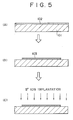
- a process of manufacturing a lightly doped drain thin film transistor of the multi-gate structure according to the present embodiment will be described in detail with reference to FIGS. 5(A) to 8(M).
- a polycrystalline silicon thin film 102 is formed with the thickness of about 75 nm on a quartz substrate 101 by the LPCVD method. If necessary, Si+ ions are implanted into the polycrystalline silicon thin film 102 to change it into an amorphous state, and then the polycrystalline silicon thin film 102 is annealed at the temperature of approximately 600 °C in a furnace to change the polycrystalline silicon into particles of large sizes.
- amorphous silicon may be formed into a film at the temperature of approximately 150 to 250 °C using the plasma chemical vapor deposition (PCVD) method.
- PCVD plasma chemical vapor deposition
- the polycrystalline silicon thin film 102 is etched into an island-like pattern.
- the polycrystalline silicon thin film 102 is oxidized to form a gate oxide film 103 with the thickness of about 60 nm on the surface thereof.
- B+ ions for adjustment of the threshold voltage for a thin film transistor are implanted.
- a nitride silicon film (Si3N4 film) 104 is formed with the thickness of about 10 to 20 nm on the gate oxide film 103 by the LPCVD method.
- the surface of the nitride silicon film 104 may be oxidized to form a SiO2 film with the thickness of about 1 to 2 nm.
- a composite gate insulator film is obtained in this manner and has a three-layer structure called ONO structure including layers of SiO2, Si3N4 and SiO2. Such structure is adopted in order to sufficiently assure a high gate voltage bearing property to enhance the reliability.
- a phosphor-doped low-resistance polycrystalline silicon film is formed with the film thickness of about 350 nm on the gate insulator film and then patterned into a predetermined pattern to form a pair of gate electrodes 105.
- the gate electrodes 105 may be formed by any of the following three methods.
- the first method involves formation of a non-doped polycrystalline silicon thin film and diffusion of phosphor from PClO3 gas into the polycrystalline silicon thin film.
- the second method involves diffusion of phosphor using a PSG film in place of PClO3 gas in the first method.
- the third method involves heat dissolution of a mixture gas of SiH4 gas and PH3 gas to form a doped polycrystalline silicon film by the LPCVD method.
- the first method was employed to manufacture the thin film transistor structure of the first embodiment described above. It is to be noted that, in the present embodiment, the gate electrodes were patterned to set the channel length L of each thin film transistor to 3 ⁇ m and the channel width W to 3 ⁇ m. Subsequently, lightly doped drain regions are formed at a step F illustrated in FIG. 6(F). In order to form lightly doped drain regions, when the thin film transistor to be formed is an n-channel thin film transistor, after the gate electrodes 105 are formed, As+ or P+ ions are implanted at a dose rate of 0.5 to 1.5 x 10¹³ /cm2.
- the thin film transistor to be formed is a p-channel thin film transistor
- B+ ions should be implanted at a doze rate of 0.1 to 2.0 x 10¹³ /dm2 similarly in place of As+ or P+ ions.
- the Si3N4 film 104 is cut along the peripheries of the gate electrodes 105 into predetermined shapes.
- a resist film 107 is formed so that the ranges of 1 ⁇ m from the opposite sides of the gate electrodes 105 may be left as lightly doped drain regions 106.
- ions of an impurity are implanted at a doze rate of 1 to 3 x 10¹⁵ /cm2 to form a source region and a drain region.
- As+ or P+ ions are implanted, but when the thin film transistor to be formed is a p-channel thin film transistor, B+ ions are implanted.
- the lengthwise dimension of the lightly doped drain regions 106 is not limited to 1 ⁇ m, it should be 0.5 ⁇ m or more with thin film transistors for switching elements for picture elements for which reduction of the leak current is required severely.
- a first interlayer insulator film 108 made of a PSG is formed with the thickness of about 600 nm by the LPCVD method, and then nitrogen atmosphere annealing is formed for 10 minutes at 1,000 °C to activate the source region, the drain region and the lightly doped drain regions.
- a contact hole 109 is formed at a predetermined location of the first interlayer insulator film 108.
- a step K illustrated in FIG. 8(K) metal aluminum to make a wiring electrode 110 is deposited with the thickness of about 600 nm and patterned.
- a second interlayer insulator film 111 made of a PSG is formed with the thickness of about 400 nm on the second interlayer insulator film 111.
- a nitride silicon film (P-SiNx film) 112 is formed with the thickness of about 100 nm by the PCVD method. Since the P-SiNx film 112 contains a large amount of water, hydrogen can be diffused into the thin film transistor effectively by performing annealing after formation of the P-SiNx film 112.
- the defect density of the polycrystalline silicon film 102 can be reduced to suppress the leak current of the thin film transistor arising from a defect.
- the P-SiNx film 112 is removed entirely by etching to open the contact hole 109, and then a transparent conductor film of an ITO or a like material is formed with the thickness of about 150 nm. Then, the ITO film is patterned into a predetermined shape to obtain a picture element electrode 113.
- the channel length of each thin film transistor was set to 3 ⁇ m; the channel width was set to 3 ⁇ m; and the length of the lightly doped drain regions was set to 1 ⁇ m
- the dimensions of the thin film transistors are not limited to those specific values.
- the gate electrode of the thin film transistor is made of polycrystalline silicon and the gate insulator film has a multi-layer structure while metal aluminum is used for the wiring electrode
- the present invention is not limited to the specific construction.
- the gate electrode may be made of such a metal as a silicide, polycide, Ta, Al, Cr, Mo or Ni or an alloy of those metals.
- the present invention can be applied to thin film transistors of any of the planar type, the regular stagger type and the reverse stagger type.
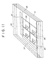
- the liquid crystal display device has a structure of an active matrix substrate 21 and an opposing substrate 22 adhered to each other with a spacer 23 interposed between them.
- a liquid crystal layer is filled between the substrates 21 and 22.
- a liquid crystal display section 26 and peripheral driver circuit sections 27 connected to the liquid crystal display section 26 are formed on the surface of the active matrix substrate 21.
- the liquid crystal display section 26 includes picture element electrodes 24 arranged in a matrix and switching elements 25 for driving the picture electrodes 24.
- the switching elements 25 are constituted from lightly doped drain thin film transistors of the multi-gate structure. Or in some cases, the thin film transistors constituting the peripheral driver circuits 27 may have such structure. Meanwhile, opposing electrodes are formed on the inner surface of the opposing substrate 22.
- liquid crystal display device of the active matrix type according to a second preferred embodiment of the present invention.
- the liquid crystal display device of the present embodiment is improved particularly in structure for suppressing the leak current of thin film transistors thereof which arises from ac driving.
- a current leaking phenomenon of a thin film transistor which relies upon the polarity upon ac driving will be described briefly with reference to FIG. 15.
- the potential at the picture element electrode relative to the potential VCOM at the opposing electrode repeats a cycle of charging and holding of the positive polarity and charging and holding of the negative polarity, and each of the picture element electrode side and the input signal line side of each thin film transistor alternately serves as the source and the drain. It has been found out that the leak current between the source and the drain is different whether the positive polarity or the negative polarity is held.
- the potential difference between the picture element electrode and the gate electrode of the thin film transistor since, during holding of the positive polarity, a high signal voltage V H is written into the picture element electrode, a large potential difference is produced from the gate voltage V GOFF in an off state through the holding time.
- the leak current flowing through the defect level in the polycrystalline silicon film is much higher during holding of the positive polarity than during holding of the negative polarity, and consequently, the picture element potential written cannot be held sufficiently, resulting in appearance as a brightness point defect.
- a thin film transistor is formed asymmetrically in structure in order to suppress the leak current of the picture element electrode side, there is a problem in that, since the degree of freedom in designing a picture element switching thin film transistor decreases, it cannot be avoided to sacrifice the open area rate of the liquid crystal picture element or that the on-current of the thin film transistor cannot be assured sufficiently, resulting in insufficient writing of the picture element potential. Accordingly, the second embodiment described below solves the problem just mentioned and achieves high on-current and low leak current simultaneously without sacrificing the degree of freedom in designing a thin film transistor.
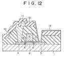
- FIG. 16 shows the liquid crystal display device of the active matrix type of such second embodiment and is a partial sectional view showing a thin film transistor and associated elements in an enlarged scale.
- the thin film transistor shown is an n-channel thin film transistor and constitutes a switching element for driving a picture element of the liquid crystal display device of the active matrix type.
- a polycrystalline silicon film is formed in a pattern on a quartz substrate 1.
- the polycrystalline silicon film has formed therein a source region 3, a source/drain region 4, a drain region 5, and a pair of channel regions 2 which are located between the source region 3 and the source/drain region 4 and between the source/drain region 4 and the drain region 5.
- a total of four low density impurity regions or lightly doped drain regions 61 to 64 of the same conductivity type as that of the source region 3 and the drain region 5 are formed between the source region 3 and source/drain region 4 and one of the channel regions 2 located between the source region 3 and the source/drain region 4 and between the source/drain region 4 and drain region 5 and the other channel region 2 located between the source/drain region 4 and the drain region 5.
- a gate electrode 9 is formed above each of the channel regions 2 with a gate insulator film interposed therebetween.
- the gate insulator films have a two-layer structure including a gate oxide film 7 and a gate nitride film 8.
- the quartz substrate 1 is covered with a first interlayer insulator film 10 made of a PSG or a like material.
- a wiring electrode 11 made of aluminum or a like material is electrically connected to the source region 3 through a contact hole formed in the first interlayer insulator film 10.
- a picture element electrode 13 made of an ITO or a like material is electrically connected to the drain region 5 through another contact hole formed similarly in the first interlayer insulator film 10.
- the picture element electrode 13 is formed on the second interlayer insulator film 12.
- the liquid crystal display device of the present embodiment is characterized in that at least one of a plurality of lightly doped drain regions formed on a plurality of thin film transistors has a length different from that of the other lightly doped drain regions.
- the length of the first and second lightly doped drain regions 61 and 62 is set to 1 ⁇ m; the length of the third lightly doped drain region 63 is set to 0.5 ⁇ m; and the length of the fourth lightly doped drain region 64 is set to 1.5 ⁇ m.
- the reason why the length of the fourth lightly doped drain region 64 is set to 1.5 ⁇ m is that it is intended to suppress the leak current on the picture element electrode side.
- the length of the third lightly doped drain region 63 is set to 0.5 ⁇ m is that it is intended to compensate for a drop of the on-current, which arises from the fact that the fourth lightly doped drain region 64 is set longer than the other lightly doped drain regions, to assure sufficiently high writing current. Even if the length of the third lightly doped drain region 63 is decreased to 0.5 ⁇ m, there is no possibility that the leak current may increase. It has been made clear by an analysis that, when the picture element electrode side holds a potential of the positive polarity, the highest electric field is applied to the fourth lightly doped drain region 64 as described hereinabove.
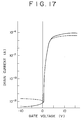
- FIG. 17 is a graph showing a gate voltage-drain current curve of an n-channel thin film transistor of the lightly doped drain type manufactured in accordance with the second embodiment described above.
- a solid line indicates a characteristic curve of the thin film transistor in the second embodiment while a broken line indicates a characteristic curve of a conventional thin film transistor.
- the conventional thin film transistor is a single gate thin film transistor of the lightly doped drain type wherein the channel length L is 5 ⁇ m; the channel width W is 3 ⁇ m; the lightly doped drain length is 1 ⁇ m; and the lightly doped drain density is 1 x 1013 cm ⁇ 2.
- a measurement was conducted with the picture element electrode caused to operate as the drain with both of the thin film transistors.
- the drain voltage was 10 V.
- the thin film transistor in the second embodiment has a very superior characteristic in that the leak current thereof is lower by one column and the on-current is higher by twice or more than the conventional thin film transistor.
- a polycrystalline silicon thin film 202 is formed with the thickness of about 75 nm on a quartz substrate 201 by the LPCVD method. If necessary, Si+ ions are implanted into the polycrystalline silicon thin film 202 to change it into an amorphous state, and then the polycrystalline silicon thin film 202 is annealed at the temperature of approximately 600 °C in a furnace to change the polycrystalline silicon into particles of large sizes. It is to be noted that, where amorphous silicon is formed from the beginning, it may be formed into a film at the temperature of approximately 150 to 250 °C using the PCVD method.
- the polycrystalline silicon thin film 202 is etched into a pattern in accordance with a thin film transistor to be formed. Then, the polycrystalline silicon thin film 202 is oxidized to form a gate oxide film 203 with the thickness of about 60 nm. Thereafter, a Si3N4 film 204 is formed with the thickness of about 10 to 20 nm on the gate oxide film 203 by the LPCVD method. In some cases, the surface of the Si3N4 film 204 may be oxidized to form a SiO2 film with the thickness of about 1 to 2 nm.
- a gate insulator film is obtained in this manner and has a three-layer structure called ONO structure including layers of SiO2, Si3N4 and SiO2.
- the structure is adopted in order to sufficiently assure a high gate voltage bearing property to enhance the reliability.
- B+ ions are implanted at a doze rate of about 1 to 8 x 1018 cm ⁇ 2 if necessary.
- a phosphor-doped low-resistance polycrystalline silicon film is formed with the film thickness of about 350 nm on the gate insulator film to form a gate electrode 205.
- the gate electrode 205 may be formed by any of the following three methods.
- the first method involves formation of a non-doped polycrystalline silicon thin film and diffusion of phosphor from PClO3 gas into the polycrystalline silicon thin film.
- the second method involves diffusion of phosphor using a PSG film in place of PClO3 gas in the first method.
- the third method involves heat dissolution of a mixture gas of SiH4 gas and PH3 gas to form a doped polycrystalline silicon film by the LPCVD method. While any one of the methods may be employed, the first method was employed to manufacture the thin film transistor structure of the second embodiment described above. It is to be noted that, in the present embodiment, the channel length L of the double-gate thin film transistor was set to 3 ⁇ m and the channel width W was set to to 3 ⁇ m. Subsequently, lightly doped drain regions 206 are formed.
- the thin film transistor to be formed is an n-channel thin film transistor
- As+ or P+ ions are implanted at a doze rate of 0.5 to 1.5 x 2013 /cm2.
- B+ ions should be implanted at a doze rate of 0.1 to 2.0 x 2013 /dm2 similarly in place of As+ or P+ ions.
- the Si3N4 film 204 is cut along the peripheries of the gate electrodes 205 into predetermined shapes.
- a resist film 207 is formed so that the ranges of a predetermined length from the opposite sides of the gate electrode 205 may be left. Subsequently, As+ or P+ ions are implanted at a doze rate of 1 to 3 x 2015 /cm2 to form a source region and a drain region in order to form an n-channel thin film transistor. It is to be noted that, when a p-channel thin film transistor is to be formed, B+ ions are implanted.
- the shape of a pattern for the resist film 207 is suitably set so as to leave lightly doped drain regions having a desired lengthwise dimension.
- the length of the first and second lightly doped drain regions 208 and 209 is 1 ⁇ m; the length of the third lightly doped drain region 210 is 0.5 ⁇ m; and the length of the fourth lightly doped drain region 211 is 1.5 ⁇ m.
- a first PSG film 212 is formed with the thickness of about 600 nm by the LPCVD method, and then N2 annealing is performed for 10 minutes at 1,000 °C to activate the source region, the drain region and the lightly doped drain regions. Then, a contact hole 213 is formed in the first PSG film 212.
- a wiring electrode 214 is formed with the thickness of about 600 nm and patterned.
- a second PSG film 215 is formed with the thickness of about 400 nm on the aluminum film.
- a nitride silicon film (P-SiNx film) 216 is formed with the thickness of about 100 nm by the PCVD method. Since the P-SiNx film 216 contains a large amount of water, hydrogen can be diffused into the thin film transistor effectively by performing annealing after formation of the P-SiNx film 216. By such hydrogen diffusion, the defect density of the polycrystalline silicon film 202 can be reduced to suppress the leak current of the thin film transistor arising from a defect.
- the P-SiNx film 216 is removed by etching to open the contact hole, and then an ITO thin film is formed with the thickness of about 150 nm. Then, the ITO film is patterned into a predetermined shape to form a picture element electrode 217.
- FIG. 21 is a schematic sectional view of a further liquid crystal display device of the active matrix type showing a third preferred embodiment of the present invention.
- the liquid crystal display device of the present embodiment basically has a same structure as the liquid crystal display device of the second embodiment described above, and corresponding elements are denoted by common reference numerals.
- the liquid crystal display device of the present embodiment is different from the liquid crystal display device of the second embodiment in that at least one of the first to fourth lightly doped drain regions 61, 62, 63 and 64 has a different density than the other lightly doped drain regions. In contrast, all of the lightly doped drain regions 61 to 64 are set to the same length of 1.0 ⁇ m.
- the fourth lightly doped drain region 64 which is located nearest to the picture element electrode 13 has a lower density than the other lightly doped drain regions 61, 62 and 63.
- As+ or P+ ions are implanted approximately at a doze ratio of 0.1 to 0.4 x 1013 cm ⁇ 2, and then only the fourth lightly doped drain region 64 is covered with resist, whereafter As+ or P+ ions are implanted again at a dose ratio of 0.6 to 1.2 x 1013 cm ⁇ 2. Since a thin film transistor wherein only the density is low only in the fourth lightly doped drain region 64 is produced in this manner, the leak current can be suppressed low.
- the first to fourth lightly doped drain regions have an equal length of 1 ⁇ m.
- the length of the third lightly doped drain region 63 may be reduced, for example, to 0.5 ⁇ m similarly as in the liquid crystal display device of the second embodiment so that high on-current may be assured while the leak current is suppressed.
- the lengths and densities of the lightly doped drain regions of the thin film transistors and the combination of them are not limited to those described above in connection with the liquid crystal display device of the second and third embodiments. This is because, if the specifications of the liquid crystal display device of the active matrix type in which thin film transistors are used are different, then the lengths and densities of the lightly doped drain regions of the thin film transistors and the combination of them should naturally be optimized accordingly. It is to be noted that, while, in the second and third embodiments described above, the channel length of the thin film transistor is set to 2.5 ⁇ m; the channel width is set to 3 ⁇ m; and the lightly doped drain length is set to 1 ⁇ m, the dimensions of the thin film transistor are not limited to the specific values.
- the degree of freedom in designing thin film transistors increases, also the degree of freedom in designing a picture element electrode pattern layout increases, and as a result, thin film transistors can be designed so that the picture element open area rate may be maximized.
- the present invention contributes also to enhancement of the open area rate of a liquid crystal display device.
- a single lightly doped drain thin film transistor having a single lightly doped drain region is employed as a picture element transistor
- most of picture element defects arising from defects of thin film transistors are thin film transistor defect modes in which the leak current in an off-state is high. It can be considered that this arises from the fact that, at a plasma step or a rubbing step in a process of manufacturing a liquid crystal display device, static electricity flows to the picture element electrode side by way of the picture element electrode to destroy the pn junction at an end of the drain of the thin film transistor.
- Such leak defects arise at the rate of 1 to several picture elements per 100,000 picture elements with a liquid crystal display device wherein picture element transistors are constituted from single lightly doped drain thin film transistors, and contrivances in manufacturing steps in the past have failed to control occurrence of static electricity and consequently failed to eliminate defects completely. Further, other than a damage caused by static electricity, also high leak current arising from crystalline defects of polycrystalline silicon used in thin film transistors is one of causes, and this cause cannot be controlled by improvement in manufacturing steps.
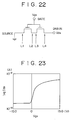
- FIG. 23 illustrates a gate voltage-drain current (V gs -I ds ) characteristic of a double lightly doped drain thin film transistor (TFT1) of a construction similar to that of the thin film transistor shown in FIG. 1.
- the double lightly doped drain thin film transistor has two lightly doped drain transistor portions of 50 ⁇ m wide and 2.5 ⁇ m long connected in series and a total of four lightly doped drain regions are provided between the source region and source/drain region and one of the two channel regions between the source region and the source/drain region and between the source/drain region and drain region and the other channel region between the source/drain region and the drain region.
- the length of the lightly doped drain regions was 1 ⁇ m. It is to be noted that, in order to facilitate a measurement of the leak current value, an experiment was conducted with the channel width increased to 16.7 times that of the actual picture element transistor.
- the positions of the lightly doped drain regions of the double lightly doped drain thin film transistor are numbered as L1, L2, L3 and L4 in order from the source side as shown in FIG. 22.
- FIG. 24 A result of the measurement is illustrated in FIG. 24. It is considered that the omission of the lightly doped drain region at the position L4 simulates damage to the thin film transistor. While the leak current in the same condition as in the case of FIG.
- TFT4 double lightly doped drain thin film transistor
- TFT4 with the lightly doped drain region at the position L2 omitted was manufactured, and a V gs -I ds characteristic of the double lightly doped drain thin film transistor was measured.
- the omission simulates damage to or a crystalline defect at the position L2 of the thin film transistor.
- the leak current in the same condition as in the case of FIG. 23 increases a little to 14.6 pA, but this is a sufficiently low value and does not make a picture element defect.
- TFT5 double lightly doped drain thin film transistor
- TFT5 with the lightly doped drain region at the position L3 omitted was manufactured, and while the polarity of the drain voltage of the thin film transistor was reversed, a V gs -I ds characteristic of the thin film transistor was measured.
- the omission is considered to simulate damage to or a crystalline defect at the position L3.
- the leak current in the same condition as in the case of FIG. 23 is 6.6 pA and equal to the leak current in the case of FIG. 23 within the range of a measurement error.
- the damage at the position L3 substantially has no influence upon the leak characteristic.
- a sixth double lightly doped drain thin film transistor (TFT6) with the two lightly doped drain regions at the positions L1 and L2 omitted and a seventh double lightly doped drain thin film transistor (TFT7) with the two lightly doped drain regions at the positions L3 and L4 omitted were manufactured, and a V gs -I ds characteristic of each of the sixth and seventh double lightly doped drain thin film transistors was measured while the polarity of the drain voltage to the seventh double lightly doped drain thin film transistor was reversed.
- the former exhibited a little increase of the leak current to 13.1 pA while this is a sufficiently low value, but the former exhibited a rather high increase to 25.5 pA while this is not sufficiently high to make a picture element defect but is sufficiently low.
- a single lightly doped drain thin film transistor (TFT8) having lightly doped drain regions of 1 ⁇ m long and having a width of 50 ⁇ m and a length of 2.5 ⁇ m was manufactured, and leak current of it was measured.
- the leak current was 24.6 pA, and a similar characteristic to that of FIG. 24 was obtained. From this fact, with a double lightly doped drain transistor, if it includes a defect at an end of the drain, the other thin film transistor portion on the source side suppresses the leak current.
- a double lightly doped drain thin film transistor (TFT9) with the lightly doped drain regions at the positions L2 and L3 omitted was manufactured, and a V gs -I ds characteristic was measured. While the leak current in the same condition as in FIG. 23 exhibits a little increase to 14.7 pA, it remains at a sufficiently low value and does not make a picture element defect. From this fact, it can be seen that, in a double lightly doped drain thin film transistor, the presence of a lightly doped drain region at an end of the drain is high in effect of suppressing the leak current and the lightly doped drain regions at the positions L2 and L3 play the role to provide some redundancy to the thin film transistor.
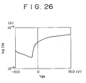
- a single lightly doped drain thin film transistor (TFT10) of the width of 50 ⁇ m and the length of 2.5 ⁇ m with the lightly doped drain region at the position 4 at an end of the drain removed was manufactured, and a V gs -I ds characteristic of it was measured and shown in FIG. 26.
- the leak current rises significantly, and in the same condition as in FIG. 23, the leak current is higher than 1 ⁇ A.
- the threshold voltage Vth is shifted to the depression side by a reduction in length of the channels, making a picture element defect. As seen from FIGS.
- the mark at the position of the lightly doped drain represents presence or absence of a lightly doped drain region at a corresponding one of the positions L1 to L4 in FIG. 22.
- the mark ⁇ represents presence of a lightly doped drain region at the position, but the mark x represents absence of a lightly doped drain region at the position, and the mark - represents absence of a thin film transistor at the position since the thin film transistor arrangement includes a single lightly doped drain thin film transistor.
- the position L2 makes a drain terminal of the thin film transistor arrangement.
- multi-gate thin film transistors having no lightly doped drain region such as a double gate thin film transistor such as, for example, the thin film transistor TFT11
- no redundancy in a thin film transistor defect can be obtained. This is because conventional multi-gate thin film transistors have been invented since a single thin film transistor cannot suppress leak current sufficiently and the requirement that "the leak current is sufficiently low using a single thin film transistor" is not satisfied.
- Redundancy constructions have conventionally been adopted in order to assure a high yield in manufacture.
- such means as provision of a plurality of thin film transistors for a single picture element or provision of an extra thin film transistor have been taken.
- those means are employed but reluctantly in order to assure an initial yield in manufacture to some degree and have, in compensation for the redundancy, several drawbacks including an increase in number of manufacturing steps, disconnection of a wiring line, an increase in number of connecting steps and complication in circuitry.
- the multi-gate lightly doped drain thin film transistor structure of the present invention has no such drawbacks at all.
- the number of manufacturing steps is not increased and there is no necessity of repairing a defect picture element or modifying a driver circuit.
- the advantages of redundancy achieved by the multi-gate lightly doped drain thin film transistor structure are very significant.
Landscapes
- Physics & Mathematics (AREA)
- Nonlinear Science (AREA)
- Mathematical Physics (AREA)
- Chemical & Material Sciences (AREA)
- Crystallography & Structural Chemistry (AREA)
- General Physics & Mathematics (AREA)
- Optics & Photonics (AREA)
- Engineering & Computer Science (AREA)
- Microelectronics & Electronic Packaging (AREA)
- Thin Film Transistor (AREA)
- Liquid Crystal (AREA)
Applications Claiming Priority (6)
| Application Number | Priority Date | Filing Date | Title |
|---|---|---|---|
| JP28046292 | 1992-09-25 | ||
| JP280462/92 | 1992-09-25 | ||
| JP28046292 | 1992-09-25 | ||
| JP2199693 | 1993-01-14 | ||
| JP21996/93 | 1993-01-14 | ||
| JP2199693 | 1993-01-14 |
Publications (3)
| Publication Number | Publication Date |
|---|---|
| EP0589478A2 true EP0589478A2 (de) | 1994-03-30 |
| EP0589478A3 EP0589478A3 (de) | 1994-11-17 |
| EP0589478B1 EP0589478B1 (de) | 1999-11-17 |
Family
ID=26359157
Family Applications (1)
| Application Number | Title | Priority Date | Filing Date |
|---|---|---|---|
| EP93115456A Expired - Lifetime EP0589478B1 (de) | 1992-09-25 | 1993-09-24 | Flüssigkristall-Anzeigevorrichtung |
Country Status (4)
| Country | Link |
|---|---|
| US (1) | US5412493A (de) |
| EP (1) | EP0589478B1 (de) |
| KR (1) | KR100292767B1 (de) |
| DE (1) | DE69327028T2 (de) |
Cited By (23)
| Publication number | Priority date | Publication date | Assignee | Title |
|---|---|---|---|---|
| FR2728390A1 (fr) * | 1994-12-19 | 1996-06-21 | Korea Electronics Telecomm | Procede de formation d'un transistor a film mince |
| EP0650197A3 (de) * | 1993-10-20 | 1997-07-09 | Semiconductor Energy Lab | Intergrierter Dünnfilm-Halbleiterschaltkreis und dessen Herstellungsverfahren. |
| EP0738012A3 (de) * | 1995-04-10 | 1997-08-13 | Canon Kk | Dünnfilmtransistor und Flüssigkristallanzeige, die diesen verwendet |
| EP0797246A1 (de) * | 1996-03-22 | 1997-09-24 | Koninklijke Philips Electronics N.V. | Herstellungsverfahren für elektronisches TFT-Bauelement |
| GB2316803A (en) * | 1996-08-24 | 1998-03-04 | Lg Electronics Inc | A thin film transistor for a liquid crystal display |
| US5729308A (en) * | 1995-02-15 | 1998-03-17 | Semiconductor Energy Laboratory Co., Ltd. | Active matrix display device |
| EP0721214A3 (de) * | 1995-01-03 | 1998-06-03 | Xerox Corporation | Schaltung mit Gitterzeilen, die an zwei oder mehr Kanalbereichen eine Halbleiterlinie kreuzt |
| GB2319889A (en) * | 1996-11-29 | 1998-06-03 | Lg Electronics Inc | Liquid crystal display and method of manufacturing the same |
| EP0871227A3 (de) * | 1997-04-08 | 1999-12-08 | Matsushita Electric Industrial Co., Ltd. | Dünnfilm-Transistor, dessen Herstellungsmethode und dessen Verwendung in einer Flüssigkeitskristallanzeige |
| EP1005093A3 (de) * | 1998-11-25 | 2001-01-31 | Sel Semiconductor Energy Laboratory Co., Ltd. | Halbleiterschaltung mit TFT |
| WO2001050514A1 (en) * | 2000-01-07 | 2001-07-12 | Seiko Epson Corporation | Thin film transistor |
| WO2001050512A1 (en) * | 2000-01-07 | 2001-07-12 | Seiko Epson Corporation | Thin-film transistor and its manufacturing method |
| US6372534B1 (en) | 1995-06-06 | 2002-04-16 | Lg. Philips Lcd Co., Ltd | Method of making a TFT array with photo-imageable insulating layer over address lines |
| EP1031873A3 (de) * | 1999-02-23 | 2005-02-23 | Sel Semiconductor Energy Laboratory Co., Ltd. | Halbleiterbauelement und Verfahren zu dessen Herstellung |
| US6909114B1 (en) | 1998-11-17 | 2005-06-21 | Semiconductor Energy Laboratory Co., Ltd. | Semiconductor device having LDD regions |
| US6979603B2 (en) | 2001-02-28 | 2005-12-27 | Semiconductor Energy Laboratory Co., Ltd. | Method of manufacturing a semiconductor device |
| US7259427B2 (en) | 1998-11-09 | 2007-08-21 | Semiconductor Energy Laboratory Co., Ltd. | Semiconductor device and method of manufacturing the same |
| US7605786B2 (en) | 1999-03-26 | 2009-10-20 | Semiconductor Energy Laboratory Co., Ltd. | Liquid crystal display device |
| US8203265B2 (en) | 1999-06-04 | 2012-06-19 | Semiconductor Energy Laboratory Co., Ltd. | Electro-optical device and electronic device |
| KR20170124523A (ko) * | 2016-04-01 | 2017-11-10 | 보에 테크놀로지 그룹 컴퍼니 리미티드 | Tft 어레이 기판, 그 제조 방법, 및 디스플레이 디바이스 |
| US10281788B2 (en) | 2007-05-17 | 2019-05-07 | Semiconductor Energy Laboratory Co., Ltd. | Liquid crystal display device |
| US10527903B2 (en) | 2002-05-17 | 2020-01-07 | Semiconductor Energy Laboratory Co., Ltd. | Display device |
| US10714622B2 (en) | 2009-10-21 | 2020-07-14 | Semiconductor Energy Laboratory Co., Ltd. | Liquid crystal display device and electronic device including the same |
Families Citing this family (99)
| Publication number | Priority date | Publication date | Assignee | Title |
|---|---|---|---|---|
| JP3437863B2 (ja) * | 1993-01-18 | 2003-08-18 | 株式会社半導体エネルギー研究所 | Mis型半導体装置の作製方法 |
| US5289030A (en) | 1991-03-06 | 1994-02-22 | Semiconductor Energy Laboratory Co., Ltd. | Semiconductor device with oxide layer |
| TW223178B (en) * | 1992-03-27 | 1994-05-01 | Semiconductor Energy Res Co Ltd | Semiconductor device and its production method |
| US6624450B1 (en) * | 1992-03-27 | 2003-09-23 | Semiconductor Energy Laboratory Co., Ltd. | Semiconductor device and method for forming the same |
| JP3587537B2 (ja) | 1992-12-09 | 2004-11-10 | 株式会社半導体エネルギー研究所 | 半導体装置 |
| US6808965B1 (en) * | 1993-07-26 | 2004-10-26 | Seiko Epson Corporation | Methodology for fabricating a thin film transistor, including an LDD region, from amorphous semiconductor film deposited at 530° C. or less using low pressure chemical vapor deposition |
| US5663077A (en) | 1993-07-27 | 1997-09-02 | Semiconductor Energy Laboratory Co., Ltd. | Method of manufacturing a thin film transistor in which the gate insulator comprises two oxide films |
| TW297142B (de) * | 1993-09-20 | 1997-02-01 | Handotai Energy Kenkyusho Kk | |
| JP3030368B2 (ja) * | 1993-10-01 | 2000-04-10 | 株式会社半導体エネルギー研究所 | 半導体装置およびその作製方法 |
| US6777763B1 (en) * | 1993-10-01 | 2004-08-17 | Semiconductor Energy Laboratory Co., Ltd. | Semiconductor device and method for fabricating the same |
| JPH07335904A (ja) | 1994-06-14 | 1995-12-22 | Semiconductor Energy Lab Co Ltd | 薄膜半導体集積回路 |
| US6897100B2 (en) | 1993-11-05 | 2005-05-24 | Semiconductor Energy Laboratory Co., Ltd. | Method for processing semiconductor device apparatus for processing a semiconductor and apparatus for processing semiconductor device |
| CN100367461C (zh) * | 1993-11-05 | 2008-02-06 | 株式会社半导体能源研究所 | 一种制造薄膜晶体管和电子器件的方法 |
| KR950021242A (ko) * | 1993-12-28 | 1995-07-26 | 김광호 | 다결정 실리콘 박막 트랜지스터 및 그 제조 방법 |
| JPH07294961A (ja) * | 1994-04-22 | 1995-11-10 | Semiconductor Energy Lab Co Ltd | アクティブマトリクス型表示装置の駆動回路および設計方法 |
| US6433361B1 (en) | 1994-04-29 | 2002-08-13 | Semiconductor Energy Laboratory Co., Ltd. | Semiconductor integrated circuit and method for forming the same |
| DE19500380C2 (de) * | 1994-05-20 | 2001-05-17 | Mitsubishi Electric Corp | Aktivmatrix-Flüssigkristallanzeige und Herstellungsverfahren dafür |
| US6133620A (en) * | 1995-05-26 | 2000-10-17 | Semiconductor Energy Laboratory Co., Ltd. | Semiconductor device and process for fabricating the same |
| CN1146056C (zh) * | 1994-06-02 | 2004-04-14 | 株式会社半导体能源研究所 | 有源矩阵显示器 |
| JP3312083B2 (ja) * | 1994-06-13 | 2002-08-05 | 株式会社半導体エネルギー研究所 | 表示装置 |
| JPH0864824A (ja) * | 1994-08-24 | 1996-03-08 | Toshiba Corp | 薄膜トランジスタおよびその製造方法 |
| US5548132A (en) * | 1994-10-24 | 1996-08-20 | Micron Technology, Inc. | Thin film transistor with large grain size DRW offset region and small grain size source and drain and channel regions |
| US5703382A (en) * | 1995-11-20 | 1997-12-30 | Xerox Corporation | Array having multiple channel structures with continuously doped interchannel regions |
| US5600155A (en) * | 1995-01-03 | 1997-02-04 | Xerox Corporation | Array with metal scan lines controlling semiconductor gate lines |
| US5557534A (en) * | 1995-01-03 | 1996-09-17 | Xerox Corporation | Forming array with metal scan lines to control semiconductor gate lines |
| US5929464A (en) * | 1995-01-20 | 1999-07-27 | Semiconductor Energy Laboratory Co., Ltd. | Active matrix electro-optical device |
| US5585292A (en) * | 1995-02-03 | 1996-12-17 | Sharp Kabushiki | Method of fabricating a thin film transistor |
| US5895766A (en) * | 1995-09-20 | 1999-04-20 | Micron Technology, Inc. | Method of forming a field effect transistor |
| JPH09146108A (ja) | 1995-11-17 | 1997-06-06 | Semiconductor Energy Lab Co Ltd | 液晶表示装置およびその駆動方法 |
| JP3963974B2 (ja) | 1995-12-20 | 2007-08-22 | 株式会社半導体エネルギー研究所 | 液晶電気光学装置 |
| KR100202231B1 (ko) * | 1996-04-08 | 1999-06-15 | 구자홍 | 액정표시장치의 제조방법 및 액정표시장치의 구조 |
| JPH09298305A (ja) * | 1996-05-08 | 1997-11-18 | Semiconductor Energy Lab Co Ltd | 薄膜トランジスタおよびかかる薄膜トランジスタを有する液晶表示装置 |
| JP3525316B2 (ja) * | 1996-11-12 | 2004-05-10 | 株式会社半導体エネルギー研究所 | アクティブマトリクス型表示装置 |
| JP3788649B2 (ja) * | 1996-11-22 | 2006-06-21 | 株式会社半導体エネルギー研究所 | 液晶表示装置 |
| KR100255591B1 (ko) * | 1997-03-06 | 2000-05-01 | 구본준 | 박막 트랜지스터 어레이의 배선 연결 구조 및 그 제조 방법 |
| TW408351B (en) | 1997-10-17 | 2000-10-11 | Semiconductor Energy Lab | Semiconductor device and method of manufacturing the same |
| US7202497B2 (en) | 1997-11-27 | 2007-04-10 | Semiconductor Energy Laboratory Co., Ltd. | Semiconductor device |
| JP4014710B2 (ja) * | 1997-11-28 | 2007-11-28 | 株式会社半導体エネルギー研究所 | 液晶表示装置 |
| US6191830B1 (en) * | 1998-03-19 | 2001-02-20 | Philips Electronics North America Corporation | Electro-optical display having split storage capacitor structure for series capacitance |
| US6140162A (en) * | 1998-06-19 | 2000-10-31 | Lg Electronics Inc. | Reduction of masking and doping steps in a method of fabricating a liquid crystal display |
| JP3421580B2 (ja) * | 1998-06-22 | 2003-06-30 | 株式会社東芝 | 撮像装置 |
| KR100336886B1 (ko) * | 1998-08-24 | 2003-06-09 | 주식회사 현대 디스플레이 테크놀로지 | 고개구율및고투과율을갖는반사형액정표시장치및그제조방법 |
| JP3141860B2 (ja) * | 1998-10-28 | 2001-03-07 | ソニー株式会社 | 液晶表示装置の製造方法 |
| US7317438B2 (en) * | 1998-10-30 | 2008-01-08 | Semiconductor Energy Laboratory Co., Ltd. | Field sequential liquid crystal display device and driving method thereof, and head mounted display |
| US7141821B1 (en) * | 1998-11-10 | 2006-11-28 | Semiconductor Energy Laboratory Co., Ltd. | Semiconductor device having an impurity gradient in the impurity regions and method of manufacture |
| US6277679B1 (en) | 1998-11-25 | 2001-08-21 | Semiconductor Energy Laboratory Co., Ltd. | Method of manufacturing thin film transistor |
| US6524895B2 (en) * | 1998-12-25 | 2003-02-25 | Semiconductor Energy Laboratory Co., Ltd. | Semiconductor device and method of fabricating the same |
| US6593592B1 (en) * | 1999-01-29 | 2003-07-15 | Semiconductor Energy Laboratory Co., Ltd. | Semiconductor device having thin film transistors |
| US6777716B1 (en) * | 1999-02-12 | 2004-08-17 | Semiconductor Energy Laboratory Co., Ltd. | Semiconductor display device and method of manufacturing therefor |
| US7821065B2 (en) | 1999-03-02 | 2010-10-26 | Semiconductor Energy Laboratory Co., Ltd. | Semiconductor device comprising a thin film transistor comprising a semiconductor thin film and method of manufacturing the same |
| KR100654927B1 (ko) * | 1999-03-04 | 2006-12-08 | 가부시키가이샤 한도오따이 에네루기 켄큐쇼 | 반도체 장치 및 그의 제작방법 |
| WO2000055681A2 (en) * | 1999-03-15 | 2000-09-21 | Sarnoff Corporation | Liquid crystal display pixel with decreased transistor voltage |
| KR100653298B1 (ko) * | 1999-03-16 | 2006-12-04 | 산요덴키가부시키가이샤 | 박막 트랜지스터의 제조 방법 |
| US7122835B1 (en) | 1999-04-07 | 2006-10-17 | Semiconductor Energy Laboratory Co., Ltd. | Electrooptical device and a method of manufacturing the same |
| US6630977B1 (en) * | 1999-05-20 | 2003-10-07 | Semiconductor Energy Laboratory Co., Ltd. | Semiconductor device with capacitor formed around contact hole |
| US6370502B1 (en) * | 1999-05-27 | 2002-04-09 | America Online, Inc. | Method and system for reduction of quantization-induced block-discontinuities and general purpose audio codec |
| KR100355713B1 (ko) * | 1999-05-28 | 2002-10-12 | 삼성전자 주식회사 | 탑 게이트 방식 티에프티 엘시디 및 제조방법 |
| US8853696B1 (en) | 1999-06-04 | 2014-10-07 | Semiconductor Energy Laboratory Co., Ltd. | Electro-optical device and electronic device |
| TW478169B (en) * | 1999-07-16 | 2002-03-01 | Seiko Epson Corp | Electro optical device and the projection display device using the same |
| TW480554B (en) | 1999-07-22 | 2002-03-21 | Semiconductor Energy Lab | Semiconductor device and manufacturing method thereof |
| JP2001175198A (ja) | 1999-12-14 | 2001-06-29 | Semiconductor Energy Lab Co Ltd | 半導体装置およびその作製方法 |
| TW525305B (en) | 2000-02-22 | 2003-03-21 | Semiconductor Energy Lab | Self-light-emitting device and method of manufacturing the same |
| US7525165B2 (en) * | 2000-04-17 | 2009-04-28 | Semiconductor Energy Laboratory Co., Ltd. | Light emitting device and manufacturing method thereof |
| JP4014831B2 (ja) * | 2000-09-04 | 2007-11-28 | 株式会社半導体エネルギー研究所 | El表示装置及びその駆動方法 |
| JP3522216B2 (ja) * | 2000-12-19 | 2004-04-26 | シャープ株式会社 | 薄膜トランジスタおよびその製造方法ならびに液晶表示装置 |
| JP4037117B2 (ja) * | 2001-02-06 | 2008-01-23 | 株式会社日立製作所 | 表示装置 |
| US7112844B2 (en) | 2001-04-19 | 2006-09-26 | Semiconductor Energy Laboratory Co., Ltd. | Semiconductor device and manufacturing method thereof |
| TW490858B (en) * | 2001-04-26 | 2002-06-11 | Samsung Electronics Co Ltd | Polycrystalline thin film transistor for liquid crystal device(LCD) and method of manufacturing the same |
| US6897477B2 (en) | 2001-06-01 | 2005-05-24 | Semiconductor Energy Laboratory Co., Ltd. | Semiconductor device, manufacturing method thereof, and display device |
| KR100469345B1 (ko) * | 2001-11-22 | 2005-02-02 | 엘지.필립스 엘시디 주식회사 | 액정 디스플레이 패널 제조방법 |
| JP2004095671A (ja) * | 2002-07-10 | 2004-03-25 | Seiko Epson Corp | 薄膜トランジスタ、スイッチング回路、アクティブ素子基板、電気光学装置、電子機器、サーマルヘッド、液滴吐出ヘッド、印刷装置、薄膜トランジスタ駆動発光表示装置 |
| US7150537B2 (en) * | 2002-08-16 | 2006-12-19 | Infocus Corporation | Projection television device and screen |
| US7233522B2 (en) * | 2002-12-31 | 2007-06-19 | Sandisk 3D Llc | NAND memory array incorporating capacitance boosting of channel regions in unselected memory cells and method for operation of same |
| US7505321B2 (en) * | 2002-12-31 | 2009-03-17 | Sandisk 3D Llc | Programmable memory array structure incorporating series-connected transistor strings and methods for fabrication and operation of same |
| US7592239B2 (en) * | 2003-04-30 | 2009-09-22 | Industry University Cooperation Foundation-Hanyang University | Flexible single-crystal film and method of manufacturing the same |
| US20040218133A1 (en) * | 2003-04-30 | 2004-11-04 | Park Jong-Wan | Flexible electro-optical apparatus and method for manufacturing the same |
| CN1300856C (zh) * | 2003-05-29 | 2007-02-14 | 友达光电股份有限公司 | 薄膜晶体管结构及其制作方法 |
| TW594653B (en) * | 2003-06-02 | 2004-06-21 | Toppoly Optoelectronics Corp | Low leakage thin film transistor circuit |
| US20050128807A1 (en) * | 2003-12-05 | 2005-06-16 | En-Hsing Chen | Nand memory array incorporating multiple series selection devices and method for operation of same |
| US7221588B2 (en) * | 2003-12-05 | 2007-05-22 | Sandisk 3D Llc | Memory array incorporating memory cells arranged in NAND strings |
| US7023739B2 (en) * | 2003-12-05 | 2006-04-04 | Matrix Semiconductor, Inc. | NAND memory array incorporating multiple write pulse programming of individual memory cells and method for operation of same |
| JP2005223047A (ja) | 2004-02-04 | 2005-08-18 | Casio Comput Co Ltd | アクティブマトリクスパネル |
| US7807516B2 (en) * | 2005-06-30 | 2010-10-05 | Semiconductor Energy Laboratory Co., Ltd. | Semiconductor device and manufacturing method of the same |
| TWI271868B (en) * | 2005-07-08 | 2007-01-21 | Au Optronics Corp | A pixel circuit of the display panel |
| TW200710471A (en) * | 2005-07-20 | 2007-03-16 | Samsung Electronics Co Ltd | Array substrate for display device |
| KR101404582B1 (ko) * | 2006-01-20 | 2014-06-09 | 가부시키가이샤 한도오따이 에네루기 켄큐쇼 | 표시장치의 구동방법 |
| US7696024B2 (en) * | 2006-03-31 | 2010-04-13 | Semiconductor Energy Laboratory Co., Ltd. | Semiconductor device and manufacturing method thereof |
| TW200805866A (en) * | 2006-07-04 | 2008-01-16 | Powertech Ind Ltd | Charger for current socket and power transmission method |
| JP4548408B2 (ja) * | 2006-11-29 | 2010-09-22 | セイコーエプソン株式会社 | 半導体装置の製造方法 |
| US20090072313A1 (en) * | 2007-09-19 | 2009-03-19 | International Business Machines Corporation | Hardened transistors in soi devices |
| WO2009096148A1 (ja) * | 2008-01-29 | 2009-08-06 | Sharp Kabushiki Kaisha | 半導体装置及びその製造方法 |
| TWI384628B (zh) * | 2008-06-27 | 2013-02-01 | 友達光電股份有限公司 | 薄膜電晶體 |
| KR20110081637A (ko) * | 2010-01-08 | 2011-07-14 | 삼성전자주식회사 | 능동형 표시 장치의 스위칭 소자 및 그 구동 방법 |
| JP2012243935A (ja) * | 2011-05-19 | 2012-12-10 | Sony Corp | デバイスおよび表示装置 |
| JP5958055B2 (ja) | 2011-07-29 | 2016-07-27 | セイコーエプソン株式会社 | 電気光学装置、電気光学装置の駆動方法および電子機器 |
| JP6436333B2 (ja) * | 2013-08-06 | 2018-12-12 | Tianma Japan株式会社 | 表示装置 |
| CN104882414B (zh) * | 2015-05-06 | 2018-07-10 | 深圳市华星光电技术有限公司 | Tft基板的制作方法及其结构 |
| CN105428370B (zh) * | 2015-11-10 | 2018-09-04 | 深圳市华星光电技术有限公司 | 液晶显示面板及液晶显示装置 |
| CN117476651B (zh) * | 2022-12-30 | 2025-09-16 | Tcl华星光电技术有限公司 | 阵列基板、显示面板及阵列基板的制备方法 |
Family Cites Families (14)
| Publication number | Priority date | Publication date | Assignee | Title |
|---|---|---|---|---|
| JPS58105574A (ja) * | 1981-12-17 | 1983-06-23 | Seiko Epson Corp | 液晶表示装置 |
| JPS58180063A (ja) * | 1982-04-15 | 1983-10-21 | Seiko Epson Corp | 薄膜トランジスタ |
| JPS58171860A (ja) * | 1982-04-01 | 1983-10-08 | Seiko Epson Corp | 薄膜トランジスタ |
| FR2524714B1 (fr) * | 1982-04-01 | 1986-05-02 | Suwa Seikosha Kk | Transistor a couche mince |
| JPS60213062A (ja) * | 1984-04-09 | 1985-10-25 | Hosiden Electronics Co Ltd | 薄膜トランジスタの製造方法 |
| US4945067A (en) * | 1988-09-16 | 1990-07-31 | Xerox Corporation | Intra-gate offset high voltage thin film transistor with misalignment immunity and method of its fabrication |
| US4907041A (en) * | 1988-09-16 | 1990-03-06 | Xerox Corporation | Intra-gate offset high voltage thin film transistor with misalignment immunity |
| JPH0338755A (ja) * | 1989-07-05 | 1991-02-19 | Nec Corp | ファイル転送システム |
| JPH03148636A (ja) * | 1989-11-06 | 1991-06-25 | Toshiba Corp | アクティブマトリクス型液晶表示素子の製造方法 |
| JP2502787B2 (ja) * | 1990-04-27 | 1996-05-29 | シャープ株式会社 | Mos型薄膜トランジスタの製造方法 |
| US5198379A (en) * | 1990-04-27 | 1993-03-30 | Sharp Kabushiki Kaisha | Method of making a MOS thin film transistor with self-aligned asymmetrical structure |
| JPH04241466A (ja) * | 1991-01-16 | 1992-08-28 | Casio Comput Co Ltd | 電界効果型トランジスタ |
| JP3072655B2 (ja) * | 1991-05-21 | 2000-07-31 | ソニー株式会社 | アクティブマトリクス表示装置 |
| JP2602132B2 (ja) * | 1991-08-09 | 1997-04-23 | 三菱電機株式会社 | 薄膜電界効果素子およびその製造方法 |
-
1993
- 1993-09-24 DE DE69327028T patent/DE69327028T2/de not_active Expired - Lifetime
- 1993-09-24 KR KR1019930019576A patent/KR100292767B1/ko not_active Expired - Lifetime
- 1993-09-24 US US08/125,802 patent/US5412493A/en not_active Expired - Lifetime
- 1993-09-24 EP EP93115456A patent/EP0589478B1/de not_active Expired - Lifetime
Cited By (75)
| Publication number | Priority date | Publication date | Assignee | Title |
|---|---|---|---|---|
| EP0650197A3 (de) * | 1993-10-20 | 1997-07-09 | Semiconductor Energy Lab | Intergrierter Dünnfilm-Halbleiterschaltkreis und dessen Herstellungsverfahren. |
| FR2728390A1 (fr) * | 1994-12-19 | 1996-06-21 | Korea Electronics Telecomm | Procede de formation d'un transistor a film mince |
| EP0721214A3 (de) * | 1995-01-03 | 1998-06-03 | Xerox Corporation | Schaltung mit Gitterzeilen, die an zwei oder mehr Kanalbereichen eine Halbleiterlinie kreuzt |
| US6417896B1 (en) * | 1995-02-15 | 2002-07-09 | Semiconductor Energy Laboratory Co., Ltd. | Active matrix display device |
| US6914642B2 (en) * | 1995-02-15 | 2005-07-05 | Semiconductor Energy Laboratory Co., Ltd. | Active matrix display device |
| US5729308A (en) * | 1995-02-15 | 1998-03-17 | Semiconductor Energy Laboratory Co., Ltd. | Active matrix display device |
| EP0738012A3 (de) * | 1995-04-10 | 1997-08-13 | Canon Kk | Dünnfilmtransistor und Flüssigkristallanzeige, die diesen verwendet |
| US5693959A (en) * | 1995-04-10 | 1997-12-02 | Canon Kabushiki Kaisha | Thin film transistor and liquid crystal display using the same |
| US6372534B1 (en) | 1995-06-06 | 2002-04-16 | Lg. Philips Lcd Co., Ltd | Method of making a TFT array with photo-imageable insulating layer over address lines |
| US6507045B2 (en) | 1995-06-06 | 2003-01-14 | Lg Philips Lcd Co., Ltd. | LCD with increased pixel opening sizes |
| US6515300B2 (en) | 1995-06-06 | 2003-02-04 | Lg. Philips Lcd Co., Ltd | Method of making a TFT array with photo-imageable insulating layer over address lines |
| US6376270B1 (en) | 1995-06-06 | 2002-04-23 | Lg. Philips Lcd Co., Ltd. | Method of making an array of TFTs having an insulation layer with a low dielectric constant |
| US6870188B2 (en) | 1995-06-06 | 2005-03-22 | Lg. Philips Lcd Co., Ltd. | LCD with increased pixel opening sizes |
| US7445948B2 (en) | 1995-06-06 | 2008-11-04 | Lg. Display Co., Ltd. | Method of making a TFT array with photo-imageable insulating layer over address lines |
| US8198110B2 (en) | 1995-06-06 | 2012-06-12 | Lg Display Co., Ltd. | Method of making a TFT array with photo-imageable insulating layer over address lines |
| US7745830B2 (en) | 1995-06-06 | 2010-06-29 | Lg Display Co., Ltd. | LCD with increased pixel opening sizes |
| US7531838B2 (en) | 1995-06-06 | 2009-05-12 | Lg Display Co., Ltd. | LCD with increased pixel opening sizes |
| EP0797246A1 (de) * | 1996-03-22 | 1997-09-24 | Koninklijke Philips Electronics N.V. | Herstellungsverfahren für elektronisches TFT-Bauelement |
| GB2316803B (en) * | 1996-08-24 | 1998-10-21 | Lg Electronics Inc | Thin film transistor liquid crystal display and method of manufacturing the same |
| US5835172A (en) * | 1996-08-24 | 1998-11-10 | Lg Electronics, Inc. | Thin film transistor liquid crystal display with main gate electrode contacting subsidiary gate electrodes and method of fabricating |
| GB2316803A (en) * | 1996-08-24 | 1998-03-04 | Lg Electronics Inc | A thin film transistor for a liquid crystal display |
| US6038008A (en) * | 1996-11-29 | 2000-03-14 | Lg Electronics Inc. | Method of making LCD having roughened steps of the protection layer |
| GB2319889B (en) * | 1996-11-29 | 1999-08-18 | Lg Electronics Inc | Liquid crystal display and method of manufacturing the same |
| GB2319889A (en) * | 1996-11-29 | 1998-06-03 | Lg Electronics Inc | Liquid crystal display and method of manufacturing the same |
| EP0871227A3 (de) * | 1997-04-08 | 1999-12-08 | Matsushita Electric Industrial Co., Ltd. | Dünnfilm-Transistor, dessen Herstellungsmethode und dessen Verwendung in einer Flüssigkeitskristallanzeige |
| US7279711B1 (en) | 1998-11-09 | 2007-10-09 | Semiconductor Energy Laboratory Co., Ltd. | Ferroelectric liquid crystal and goggle type display devices |
| US9214532B2 (en) | 1998-11-09 | 2015-12-15 | Semiconductor Energy Laboratory Co., Ltd. | Ferroelectric liquid crystal display device comprising gate-overlapped lightly doped drain structure |
| US8653595B2 (en) | 1998-11-09 | 2014-02-18 | Semiconductor Energy Laboratory Co., Ltd. | Semiconductor device and method of manufacturing the same |
| US7923779B2 (en) | 1998-11-09 | 2011-04-12 | Semiconductor Energy Laboratory Co., Ltd. | Semiconductor device and method of manufacturing the same |
| US7259427B2 (en) | 1998-11-09 | 2007-08-21 | Semiconductor Energy Laboratory Co., Ltd. | Semiconductor device and method of manufacturing the same |
| US9627460B2 (en) | 1998-11-17 | 2017-04-18 | Semiconductor Energy Laboratory Co., Ltd. | Method of fabricating a semiconductor device |
| US6909114B1 (en) | 1998-11-17 | 2005-06-21 | Semiconductor Energy Laboratory Co., Ltd. | Semiconductor device having LDD regions |
| US7172928B2 (en) | 1998-11-17 | 2007-02-06 | Semiconductor Energy Laboratory Co., Ltd. | Method of fabricating a semiconductor device by doping impurity element into a semiconductor layer through a gate electrode |
| US6365917B1 (en) | 1998-11-25 | 2002-04-02 | Semiconductor Energy Laboratory Co., Ltd. | Semiconductor device |
| US6949767B2 (en) | 1998-11-25 | 2005-09-27 | Semiconductor Energy Laboratory Co., Ltd. | Semiconductor device |
| EP1005093A3 (de) * | 1998-11-25 | 2001-01-31 | Sel Semiconductor Energy Laboratory Co., Ltd. | Halbleiterschaltung mit TFT |
| US7442991B2 (en) | 1999-02-23 | 2008-10-28 | Semiconductor Energy Laboratory Co., Ltd. | Display including casing and display unit |
| US7745829B2 (en) | 1999-02-23 | 2010-06-29 | Semiconductor Energy Laboratory Co., Ltd | Semiconductor device and fabrication method thereof |
| EP1031873A3 (de) * | 1999-02-23 | 2005-02-23 | Sel Semiconductor Energy Laboratory Co., Ltd. | Halbleiterbauelement und Verfahren zu dessen Herstellung |
| US6967129B2 (en) | 1999-02-23 | 2005-11-22 | Semiconductor Energy Laboratory Co., Ltd. | Semiconductor device and fabrication method thereof |
| US9910334B2 (en) | 1999-02-23 | 2018-03-06 | Semiconductor Energy Laboratory Co., Ltd. | Semiconductor device and fabrication method thereof |
| US8030659B2 (en) | 1999-02-23 | 2011-10-04 | Semiconductor Energy Laboratory Co., Ltd. | Semiconductor device and fabrication method thereof |
| US7365393B2 (en) | 1999-02-23 | 2008-04-29 | Semiconductor Energy Laboratory Co., Ltd. | Semiconductor device and fabrication method thereof |
| US8125429B2 (en) | 1999-03-26 | 2012-02-28 | Semiconductor Energy Laboratory Co., Ltd. | Liquid crystal display device |
| US7773066B2 (en) | 1999-03-26 | 2010-08-10 | Semiconductor Energy Laboratory Co., Ltd. | Liquid crystal display device |
| US7605786B2 (en) | 1999-03-26 | 2009-10-20 | Semiconductor Energy Laboratory Co., Ltd. | Liquid crystal display device |
| US9704444B2 (en) | 1999-03-26 | 2017-07-11 | Semiconductor Energy Laboratory Co., Ltd. | Liquid crystal display device |
| US8144278B2 (en) | 1999-03-26 | 2012-03-27 | Semiconductor Energy Laboratory Co., Ltd. | Optically compensated birefringence mode liquid crystal display device |
| US8149198B2 (en) | 1999-03-26 | 2012-04-03 | Semiconductor Energy Laboratory Co., Ltd. | Liquid crystal display device |
| US8896639B2 (en) | 1999-03-26 | 2014-11-25 | Semiconductor Energy Laboratory Co., Ltd. | Liquid crystal display device |
| US8421350B2 (en) | 1999-06-04 | 2013-04-16 | Semiconductor Energy Laboratory Co., Ltd. | Electro-optical device and electronic device |
| US9178177B2 (en) | 1999-06-04 | 2015-11-03 | Semiconductor Energy Laboratory Co., Ltd. | Electro-optical device and electronic device |
| US8987988B2 (en) | 1999-06-04 | 2015-03-24 | Semiconductor Energy Laboratory Co., Ltd. | Display device |
| US8203265B2 (en) | 1999-06-04 | 2012-06-19 | Semiconductor Energy Laboratory Co., Ltd. | Electro-optical device and electronic device |
| US8674600B2 (en) | 1999-06-04 | 2014-03-18 | Semiconductor Energy Laboratory Co., Ltd. | Display device |
| US6548356B2 (en) | 2000-01-07 | 2003-04-15 | Seiko Epson Corporation | Thin film transistor |
| US6580129B2 (en) | 2000-01-07 | 2003-06-17 | Seiko Epson Corporation | Thin-film transistor and its manufacturing method |
| GB2358083B (en) * | 2000-01-07 | 2004-02-18 | Seiko Epson Corp | Thin-film transistor and its manufacturing method |
| WO2001050514A1 (en) * | 2000-01-07 | 2001-07-12 | Seiko Epson Corporation | Thin film transistor |
| GB2358082B (en) * | 2000-01-07 | 2003-11-12 | Seiko Epson Corp | Semiconductor transistor |
| WO2001050512A1 (en) * | 2000-01-07 | 2001-07-12 | Seiko Epson Corporation | Thin-film transistor and its manufacturing method |
| US6979603B2 (en) | 2001-02-28 | 2005-12-27 | Semiconductor Energy Laboratory Co., Ltd. | Method of manufacturing a semiconductor device |
| US7531839B2 (en) | 2001-02-28 | 2009-05-12 | Semiconductor Energy Laboratory Co., Ltd. | Display device having driver TFTs and pixel TFTs formed on the same substrate |
| US8017951B2 (en) | 2001-02-28 | 2011-09-13 | Semiconductor Energy Laboratory Co., Ltd. | Semiconductor device including a conductive film having a tapered shape |
| US8242508B2 (en) | 2001-02-28 | 2012-08-14 | Semiconductor Energy Laboratory Co., Ltd. | Method of manufacturing a semiconductor device |
| US11422423B2 (en) | 2002-05-17 | 2022-08-23 | Semiconductor Energy Laboratory Co., Ltd. | Display device |
| US10527903B2 (en) | 2002-05-17 | 2020-01-07 | Semiconductor Energy Laboratory Co., Ltd. | Display device |
| US10281788B2 (en) | 2007-05-17 | 2019-05-07 | Semiconductor Energy Laboratory Co., Ltd. | Liquid crystal display device |
| US10948794B2 (en) | 2007-05-17 | 2021-03-16 | Semiconductor Energy Laboratory Co., Ltd. | Liquid crystal display device |
| US10989974B2 (en) | 2007-05-17 | 2021-04-27 | Semiconductor Energy Laboratory Co., Ltd. | Liquid crystal display device |
| US11493816B2 (en) | 2007-05-17 | 2022-11-08 | Semiconductor Energy Laboratory Co., Ltd. | Liquid crystal display device |
| US11803092B2 (en) | 2007-05-17 | 2023-10-31 | Semiconductor Energy Laboratory Co., Ltd. | Liquid crystal display device |
| US12061400B2 (en) | 2007-05-17 | 2024-08-13 | Semiconductor Energy Laboratory Co., Ltd. | Liquid crystal display device |
| US10714622B2 (en) | 2009-10-21 | 2020-07-14 | Semiconductor Energy Laboratory Co., Ltd. | Liquid crystal display device and electronic device including the same |
| KR20170124523A (ko) * | 2016-04-01 | 2017-11-10 | 보에 테크놀로지 그룹 컴퍼니 리미티드 | Tft 어레이 기판, 그 제조 방법, 및 디스플레이 디바이스 |
Also Published As
| Publication number | Publication date |
|---|---|
| US5412493A (en) | 1995-05-02 |
| DE69327028T2 (de) | 2000-05-31 |
| KR940007591A (ko) | 1994-04-27 |
| KR100292767B1 (ko) | 2001-09-17 |
| EP0589478A3 (de) | 1994-11-17 |
| DE69327028D1 (de) | 1999-12-23 |
| EP0589478B1 (de) | 1999-11-17 |
Similar Documents
| Publication | Publication Date | Title |
|---|---|---|
| EP0589478B1 (de) | Flüssigkristall-Anzeigevorrichtung | |
| JP3343160B2 (ja) | 液晶表示装置 | |
| JP3338481B2 (ja) | 液晶表示装置 | |
| US7196746B2 (en) | Pixel structure and manufacturing method thereof | |
| US6828585B2 (en) | Thin-film transistor, method for fabricating the same, and liquid crystal display device | |
| US7968387B2 (en) | Thin film transistor and method of fabricating thin film transistor substrate | |
| EP2259135A2 (de) | Halbleiterbauelement und dessen Herstellungsverfahren | |
| US8174023B2 (en) | Method of fabricating memory cell | |
| US5703382A (en) | Array having multiple channel structures with continuously doped interchannel regions | |
| JPS58105574A (ja) | 液晶表示装置 | |
| US5677547A (en) | Thin film transistor and display device including same | |
| JPH0722627A (ja) | 薄膜半導体装置及びアクティブマトリクス液晶表示装置 | |
| JPH06317812A (ja) | アクティブマトリクス素子及びその製造方法 | |
| US20060118787A1 (en) | Electronic device with electrostatic discharge protection | |
| US6847414B2 (en) | Manufacturing method for liquid crystal display | |
| JPS625661A (ja) | 薄膜トランジスタ | |
| US8279389B2 (en) | Liquid crystal display device having storage lines overlapping active layers formed of polysilicon material | |
| US9035315B2 (en) | Semiconductor device, display device, and method for manufacturing semiconductor device | |
| JPH08220506A (ja) | 液晶表示装置 | |
| JPH0864830A (ja) | アクティブマトリクス基板およびその製造方法 | |
| JP2622661B2 (ja) | 液晶表示パネル | |
| US8816437B2 (en) | Semiconductor device and method for manufacturing same | |
| JP2001318623A (ja) | アクティブマトリクス基板とその製造方法、電気光学装置とその製造方法及び電子機器 | |
| JPH03293641A (ja) | アクティブマトリクス表示装置 | |
| JP3261785B2 (ja) | 薄膜トランジスタの製造方法 |
Legal Events
| Date | Code | Title | Description |
|---|---|---|---|
| PUAI | Public reference made under article 153(3) epc to a published international application that has entered the european phase |
Free format text: ORIGINAL CODE: 0009012 |
|
| AK | Designated contracting states |
Kind code of ref document: A2 Designated state(s): DE FR GB |
|
| PUAL | Search report despatched |
Free format text: ORIGINAL CODE: 0009013 |
|
| AK | Designated contracting states |
Kind code of ref document: A3 Designated state(s): DE FR GB |
|
| 17P | Request for examination filed |
Effective date: 19950413 |
|
| 17Q | First examination report despatched |
Effective date: 19961217 |
|
| GRAG | Despatch of communication of intention to grant |
Free format text: ORIGINAL CODE: EPIDOS AGRA |
|
| GRAG | Despatch of communication of intention to grant |
Free format text: ORIGINAL CODE: EPIDOS AGRA |
|
| GRAH | Despatch of communication of intention to grant a patent |
Free format text: ORIGINAL CODE: EPIDOS IGRA |
|
| RIC1 | Information provided on ipc code assigned before grant |
Free format text: 6G 02F 1/136 A, 6H 01L 29/78 B |
|
| GRAH | Despatch of communication of intention to grant a patent |
Free format text: ORIGINAL CODE: EPIDOS IGRA |
|
| GRAA | (expected) grant |
Free format text: ORIGINAL CODE: 0009210 |
|
| AK | Designated contracting states |
Kind code of ref document: B1 Designated state(s): DE FR GB |
|
| REF | Corresponds to: |
Ref document number: 69327028 Country of ref document: DE Date of ref document: 19991223 |
|
| ET | Fr: translation filed | ||
| PLBE | No opposition filed within time limit |
Free format text: ORIGINAL CODE: 0009261 |
|
| 26N | No opposition filed | ||
| REG | Reference to a national code |
Ref country code: GB Ref legal event code: IF02 |
|
| PGFP | Annual fee paid to national office [announced via postgrant information from national office to epo] |
Ref country code: GB Payment date: 20120920 Year of fee payment: 20 |
|
| PGFP | Annual fee paid to national office [announced via postgrant information from national office to epo] |
Ref country code: DE Payment date: 20120921 Year of fee payment: 20 |
|
| PGFP | Annual fee paid to national office [announced via postgrant information from national office to epo] |
Ref country code: FR Payment date: 20121010 Year of fee payment: 20 |
|
| REG | Reference to a national code |
Ref country code: DE Ref legal event code: R071 Ref document number: 69327028 Country of ref document: DE |
|
| REG | Reference to a national code |
Ref country code: GB Ref legal event code: PE20 Expiry date: 20130923 |
|
| PG25 | Lapsed in a contracting state [announced via postgrant information from national office to epo] |
Ref country code: DE Free format text: LAPSE BECAUSE OF EXPIRATION OF PROTECTION Effective date: 20130925 |
|
| PG25 | Lapsed in a contracting state [announced via postgrant information from national office to epo] |
Ref country code: GB Free format text: LAPSE BECAUSE OF EXPIRATION OF PROTECTION Effective date: 20130923 |