EP0590627B1 - Masque pour la fabrication de semi-conducteurs - Google Patents
Masque pour la fabrication de semi-conducteurs Download PDFInfo
- Publication number
- EP0590627B1 EP0590627B1 EP93115697A EP93115697A EP0590627B1 EP 0590627 B1 EP0590627 B1 EP 0590627B1 EP 93115697 A EP93115697 A EP 93115697A EP 93115697 A EP93115697 A EP 93115697A EP 0590627 B1 EP0590627 B1 EP 0590627B1
- Authority
- EP
- European Patent Office
- Prior art keywords
- phase shift
- mask
- opaque
- areas
- pattern
- Prior art date
- Legal status (The legal status is an assumption and is not a legal conclusion. Google has not performed a legal analysis and makes no representation as to the accuracy of the status listed.)
- Expired - Lifetime
Links
Images


Classifications
-
- G—PHYSICS
- G03—PHOTOGRAPHY; CINEMATOGRAPHY; ANALOGOUS TECHNIQUES USING WAVES OTHER THAN OPTICAL WAVES; ELECTROGRAPHY; HOLOGRAPHY
- G03F—PHOTOMECHANICAL PRODUCTION OF TEXTURED OR PATTERNED SURFACES, e.g. FOR PRINTING, FOR PROCESSING OF SEMICONDUCTOR DEVICES; MATERIALS THEREFOR; ORIGINALS THEREFOR; APPARATUS SPECIALLY ADAPTED THEREFOR
- G03F1/00—Originals for photomechanical production of textured or patterned surfaces, e.g., masks, photo-masks, reticles; Mask blanks or pellicles therefor; Containers specially adapted therefor; Preparation thereof
- G03F1/26—Phase shift masks [PSM]; PSM blanks; Preparation thereof
- G03F1/29—Rim PSM or outrigger PSM; Preparation thereof
Definitions
- This invention relates to semiconductor circuit fabrication, and more particularly to a method of making a mask for use in lithographic semiconductor fabrication, which provides phase shift boundaries of the mask features.
- Microcircuit fabrication requires that precisely controlled quantities of impurities be introduced into tiny regions of a silicon substrate, and subsequently interconnected.
- the patterns that define these regions are created by lithographic processes.
- the first basic step of the lithographic process is applying a photoresist material as a thin film to the substrate, i.e., an oxide layer on silicon.
- the photoresist layer is then exposed through a mask, which contains dear and opaque features that define the pattern to be created on the photoresist layer.
- the areas in the photoresist that are exposed to the light are made either soluble or insoluble in a specific solvent known as a developer.
- the regions of the substrate no longer covered by the resist are removed by etching, thereby replicating the mask pattern in the oxide layer.
- phase shift masks instead of using a single clear edge area to bound opaque regions, a series of two clear edge areas are used. The result is a double boundary, with a first boundary zone transmitting light of one phase, and an second boundary zone transmitting light of a phase that is 180 degrees different.
- the result is that the edges of opaque regions are defined with an intensity curve that is much steeper than would occur at a single boundary zone of a non phase shifting mask.
- the boundaries having these steep intensity curves are referred to as a "high contrast boundaries".
- This high contrast effect can be used to make resist edges with steeper walls.
- shapes, such as lines and spaces having much finer resolution than is possible with non phase shifting masks. For example, lines and spaces can be made much narrower and more dense.
- phase shift mask with self-aligned phase shift boundaries is known.
- a light shielding film is produced on the entire surface of a transparent substrate, and a photoresist pattern is produced thereon.
- the partially completed device is over-etched using that photoresist pattern as a mask to produce a light shielding film pattern having a desired width, and a transparent thin film pattern is produced at an aperture section of the light shielding film pattern, separated from the light shielding film pattern, by depositing a transparent thin film shifting the phase of the exposure light on the entire surface and carrying out lift-off.
- phase shifting masks with self-aligned phase shift boundaries are known, wherein side-etching of a light shielding pattern is carried out before deposition of the phase shifting material in order to achieve self-alignment of the phase shift boundaries.
- US-A-5 045 417 discloses a method of forming a phase shift mask, wherein a transparent phase shifting film is formed in such a manner that it covers a light shielding pattern along a pattern formed by magnifying or demagnifying the light shielding pattern or transmission pattern.
- EP-A-0 395 425 discloses a method of making a mask, which comprises the steps of forming an opaque pattern layer on a transparent layer which is transparent with respect to a light which is used for an exposure, forming a stopper layer on the opaque pattern layer, forming a phase shift layer which transmits the light on the opaque pattern layer to a predetermined thickness, so that a phase shift occurs between a phase of the light transmitted through the phase shift layer and a phase of the light transmitted through a portion of the mask having no phase shift layer, forming a resist pattern which is made of a resist material on the phase shift layer, and etching the phase shift layer using the stopper layer as an etching stopper and the resist pattern as an etching mask so that the phase shift layer remains on the stopper layer only in a vicinity of an edge portion of the opaque pattern layer in at least one part of the mask.
- phase shifting masks are useful only as positive tone masks. Also, some are difficult to repair, especially those having the opaque areas fabricated on top of phase shifting areas.
- Figure 1 is a top plan view of a portion of a mask 10, such as might be used for semiconductor lithography.
- Mask 10 has a pattern of shapes that are either opaque or clear. For purposes of example herein, these shapes are alternating opaque lines 12 and clear spaces 14.
- the spaces 14 have two zones 14a and 14b, which have different thicknesses.
- the geometries of the shapes on mask 10 are not important to the invention, expect insofar as any edge of an opaque shape is bounded first by a clear thin zone 14a and then by a clear thick zone 14b.
- the thin zone 14a is mask glass, covered by a clear etch stop layer (not shown).
- the thick zone 14b is mask glass, also covered by the etch stop layer, as well as by phase shifter material.
- the thin zone 14a forms a first boundary 15a with opaque area 12, and the thick zone 14b forms a second boundary 15b with the thin zone 14a. This second boundary 15b is where the phase shift of the transmitted light occurs.
- the opaque areas 12 of mask 10 may be any type of known light blocking material, known in the art of photomasking.
- An example of a suitable material is chrome.
- the mask glass may be any type of known mask glass.
- the phase shift glass may be the same type of material as the mask glass, but with a thickness that is calculated to provide the desired phase difference.
- a feature of mask 10 is that its clear zones 14a and 14b are self-aligned with respect to its opaque areas 12.
- the invention ensures that each distance, d, is the same, such that the phase shift boundary 15b occurs at the same distance from any two adjacent edges of opaque areas.
- each thick zone 14b is centered between opaque lines 12.
- Figures 2A - 2C illustrate the effect of the different areas of mask 10 on incident light. As shown in Figure 2A, opaque areas 12 do not transmit any light.
- the clear zones 14a and 14b which have two different thicknesses, transmit light to an imaging surface 20, such as a semiconductor wafer-in-process.
- the solid line of Figure 2C illustrates the intensity curve of the transmitted light as received at the imaging surface 20.
- the dotted line illustrates the intensity curve that would occur if a single, non phase shifting, clear boundary were used. As indicated, the phase shifted curve is steeper than would occur at boundary 15a if boundary 15b were not also present.
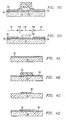
- Figures 3A - 3H illustrate the process of making a space 14 in a phase shift mask 10 in accordance with the invention.
- the steps illustrated in Figures 3A - 3C are like those of conventional mask fabrication. However, the steps shown in Figure 3D - 3H include the formation of an etch stop layer 34, thin zones 14a, and thick zones 14b that exhibit the self-alignment feature of the invention.
- Figure 3A illustrates a mask blank.
- the mask blank may be any conventional mask blank having two layers, a transparent layer 31 and an opaque layer 32.
- transparent layer 31 is glass and opaque layer 32 is chrome.
- Figure 3C illustrates the resist pattern transfer to the opaque layer 32. Typically, this is accomplished with wet etching.
- the opaque layer 32 now defines a pattern of opaque areas 12, such as those illustrated in Figures 1 and 2A.
- Figure 3E illustrates the deposition of a phase shifter layer 35 above etch stop layer 34.
- the material used for phase shift layer 35 is any light transmitting material.
- the material used for phase shift layer 35 does not have the etch resistant characteristic of etch stop layer 34.
- An example of a suitable material is silicon oxide.
- Phase shifter layer 35 may be the same material as mask glass 31, such that the controlling factor in determining the phase difference between phase shifter zones 14b and mask glass zones 14a is their relative thickness.
- Figure 3G illustrates the etching process, whereby the non exposed areas of photoresist layer 36 are removed, as well as areas of shifter layer 35 that are not covered by exposed areas of photoresist layer 36.
- the etching is a wet etch that is chosen so as to not affect etch stop layer 34.
- the etching tends to etch away phase shift layer 35 under the edges of the exposed areas of photoresist layer 36, such when etching is stopped, the remaining areas of phase shift layer 35 are narrower than the overlying exposed areas of resist layer 36. As a result, at every edge of an opaque area, the etching continues laterally outward for some predetermined distance, d. However, downward etching toward mask glass layer 31 is stopped at etch stop layer 34. Etch stop layer 34 remains intact.
- Figures 4A - 4H are similar to Figures 3A - 3H, except that they illustrate the formation of an opaque line 12 rather than a clear space 14. As in Figure 3H, after fabrication, the edges of the opaque areas 12 are defined by a phase shifting boundary 15b. A distance, d, defines a thin zone 14a on either side of the line 12, and d is the same on both sides.
- an advantage of the invention is that where the opaque areas are to define lines and spaces, or any other feature, the phase shift zones 14a and 14b are self-aligned with respect to the feature edges.
- the distance, d, that defines the width of the thin zone 14a, i.e., the distance to the phase shifting boundary 15b, is the same on each side of the opaque area 12 or clear space 14. This is an inherent result of the wet etching steps of Figures 3G and 4G.
- Another advantage of the invention is that repairs may be easily made during fabrication of any layer. Defects in the pattern of opaque layer 32 can be repaired before the etch stop layer 34 is deposited. There is no underlying layer that needs to remain undisturbed. The etch stop layer 34 can be repaired by using an etch that will not affect the mask glass 31. Similarly, defects in the phase shift layer 35 can be etched off by using an etch that will not disturb etch stop layer 34.
Landscapes
- Physics & Mathematics (AREA)
- General Physics & Mathematics (AREA)
- Preparing Plates And Mask In Photomechanical Process (AREA)
Claims (4)
- Procédé de fabrication d'un masque destiné à être utilisé lors d'une fabrication lithographique de semiconducteur, qui fournit des limites de déphasage des éléments du masque, comprenant les étapes de :fabrication d'une configuration de matériau opaque sur la surface d'un substrat (31) de masque en verre, la configuration étant constituée de zones (12) du matériau opaque (32) séparées par des zones claires (14) dans lesquelles le verre de masque (31) n'est pas recouvert par le matériau opaque (32) ;dépôt d'une couche (34) d'arrêt de gravure recouvrant le matériau opaque (32) et les zones claires (14), la couche (34) d'arrêt de gravure étant capable de transmettre la lumière ;fabrication d'une configuration de matériau de déphasage sur la surface de la couche (34) d'arrêt de gravure, dans des zones non recouvertes par le matériau opaque (32), le matériau (35) de déphasage étant espacé des bords des zones opaques (12) de telle sorte que chacun des bords est limité par une zone mince (14a) du verre de masque (31) recouverte par la couche (34) d'arrêt de gravure et ensuite par une zone épaisse (14b) du verre de masque (31) recouverte par la couche (34) d'arrêt de gravure et le matériau de déphasage (35) ; etdans lequel la fabrication de la configuration du matériau de déphasage comprend la fabrication par des procédés de photorésist et de gravure humide, la photogravure éliminant des zones du matériau (35) de déphasage non recouvertes par un matériau de photorésist exposé (36), et est commandée de telle sorte que la gravure peut se poursuivre vers le bas le long des bords des zones opaques (12), de manière à définir les zones minces (14a).
- Procédé selon la revendication 1, dans lequel la fabrication de la configuration de matériau opaque comprend la fabrication de la configuration par des procédés conventionnels de photorésist et de gravure.
- Procédé selon la revendication 1 ou la revendication 2, comprenant en outre le dépôt de la couche (34) d'arrêt de gravure avec un processus de dépôt chimique en phase vapeur.
- Procédé selon l'une quelconque des revendications 1 à 3, comprenant en outre le dépôt du matériau de déphasage (35) sur une épaisseur calculée pour conduire à une lumière transmise avec une différence de phase de 180 degrés par rapport à la lumière transmise par l'intermédiaire du verre de masque (31).
Applications Claiming Priority (2)
| Application Number | Priority Date | Filing Date | Title |
|---|---|---|---|
| US95419292A | 1992-09-29 | 1992-09-29 | |
| US954192 | 1992-09-29 |
Publications (3)
| Publication Number | Publication Date |
|---|---|
| EP0590627A2 EP0590627A2 (fr) | 1994-04-06 |
| EP0590627A3 EP0590627A3 (en) | 1996-08-07 |
| EP0590627B1 true EP0590627B1 (fr) | 2001-01-03 |
Family
ID=25495070
Family Applications (1)
| Application Number | Title | Priority Date | Filing Date |
|---|---|---|---|
| EP93115697A Expired - Lifetime EP0590627B1 (fr) | 1992-09-29 | 1993-09-29 | Masque pour la fabrication de semi-conducteurs |
Country Status (5)
| Country | Link |
|---|---|
| EP (1) | EP0590627B1 (fr) |
| JP (1) | JPH06266094A (fr) |
| KR (1) | KR940007984A (fr) |
| DE (1) | DE69329813T2 (fr) |
| TW (1) | TW302500B (fr) |
Families Citing this family (1)
| Publication number | Priority date | Publication date | Assignee | Title |
|---|---|---|---|---|
| JP2773718B2 (ja) * | 1995-11-29 | 1998-07-09 | 日本電気株式会社 | フォトマスクおよびパターン形成方法 |
Citations (1)
| Publication number | Priority date | Publication date | Assignee | Title |
|---|---|---|---|---|
| EP0395425A2 (fr) * | 1989-04-28 | 1990-10-31 | Fujitsu Limited | Masque, procédé de fabrication et procédé pour la fabrication d'un dessin utilisant ce masque |
Family Cites Families (3)
| Publication number | Priority date | Publication date | Assignee | Title |
|---|---|---|---|---|
| JP2710967B2 (ja) * | 1988-11-22 | 1998-02-10 | 株式会社日立製作所 | 集積回路装置の製造方法 |
| EP0437376B1 (fr) * | 1990-01-12 | 1997-03-19 | Sony Corporation | Masque à décalage de phase et méthode de fabrication |
| JPH0450943A (ja) * | 1990-06-15 | 1992-02-19 | Mitsubishi Electric Corp | マスクパターンとその製造方法 |
-
1993
- 1993-09-28 KR KR1019930020079A patent/KR940007984A/ko not_active Ceased
- 1993-09-28 JP JP24181593A patent/JPH06266094A/ja active Pending
- 1993-09-29 EP EP93115697A patent/EP0590627B1/fr not_active Expired - Lifetime
- 1993-09-29 DE DE69329813T patent/DE69329813T2/de not_active Expired - Fee Related
-
1994
- 1994-08-22 TW TW083107651A patent/TW302500B/zh active
Patent Citations (1)
| Publication number | Priority date | Publication date | Assignee | Title |
|---|---|---|---|---|
| EP0395425A2 (fr) * | 1989-04-28 | 1990-10-31 | Fujitsu Limited | Masque, procédé de fabrication et procédé pour la fabrication d'un dessin utilisant ce masque |
Also Published As
| Publication number | Publication date |
|---|---|
| EP0590627A2 (fr) | 1994-04-06 |
| KR940007984A (ko) | 1994-04-28 |
| JPH06266094A (ja) | 1994-09-22 |
| EP0590627A3 (en) | 1996-08-07 |
| TW302500B (fr) | 1997-04-11 |
| DE69329813D1 (de) | 2001-02-08 |
| DE69329813T2 (de) | 2001-05-23 |
Similar Documents
| Publication | Publication Date | Title |
|---|---|---|
| US5888674A (en) | Method of manufacturing a halftone phase shift mask | |
| JP2739065B2 (ja) | アパーチャ交番移相マスクを製造する方法 | |
| US5881125A (en) | Attenuated phase-shifted reticle using sub-resolution pattern | |
| KR100201040B1 (ko) | 위상 쉬프트 마스크 및 그 제조 방법 | |
| US5153083A (en) | Method of making phase-shifting lithographic masks | |
| EP0453310B1 (fr) | Masque pour photolithographie | |
| GB2291266A (en) | Submicroscopic pattern formation on semiconductors | |
| KR100271699B1 (ko) | 포토마스크 및 포토마스크를 사용하는 반도체장치의 제조방법 | |
| US5888678A (en) | Mask and simplified method of forming a mask integrating attenuating phase shifting mask patterns and binary mask patterns on the same mask substrate | |
| US5292623A (en) | Method for forming integrated circuit devices using a phase shifting mask | |
| KR100399533B1 (ko) | 광학리소그래픽마스크및그의제조방법 | |
| US5695896A (en) | Process for fabricating a phase shifting mask | |
| US5533634A (en) | Quantum chromeless lithography | |
| US5322748A (en) | Photomask and a method of manufacturing thereof comprising trapezoidal shaped light blockers covered by a transparent layer | |
| US5698349A (en) | Sub-resolution phase shift mask | |
| GB2302962A (en) | Phase shift mask | |
| US5556725A (en) | Method for fabricating a half-tone type phase shift mask | |
| JPH10123697A (ja) | 位相シフトマスク及びその製造方法 | |
| US5543254A (en) | Phase shift mask and method for fabricating the same | |
| EP0590627B1 (fr) | Masque pour la fabrication de semi-conducteurs | |
| EP0553543B1 (fr) | Masque à décalage de phase et méthode pour former un motif dans une photoréserve en utilisant ce masque | |
| JPH07219206A (ja) | フォトマスク | |
| US20040023129A1 (en) | Method of manufacturing phase shift mask and phase shift mask | |
| US6479194B1 (en) | Transparent phase shift mask for fabrication of small feature sizes | |
| EP0738925A2 (fr) | Masque pour l'ajustement de la largeur de ligne d'un motif de photoréserve |
Legal Events
| Date | Code | Title | Description |
|---|---|---|---|
| PUAI | Public reference made under article 153(3) epc to a published international application that has entered the european phase |
Free format text: ORIGINAL CODE: 0009012 |
|
| AK | Designated contracting states |
Kind code of ref document: A2 Designated state(s): DE FR GB IT NL |
|
| PUAL | Search report despatched |
Free format text: ORIGINAL CODE: 0009013 |
|
| AK | Designated contracting states |
Kind code of ref document: A3 Designated state(s): DE FR GB IT NL |
|
| 17P | Request for examination filed |
Effective date: 19970130 |
|
| 17Q | First examination report despatched |
Effective date: 19970305 |
|
| GRAG | Despatch of communication of intention to grant |
Free format text: ORIGINAL CODE: EPIDOS AGRA |
|
| GRAG | Despatch of communication of intention to grant |
Free format text: ORIGINAL CODE: EPIDOS AGRA |
|
| GRAH | Despatch of communication of intention to grant a patent |
Free format text: ORIGINAL CODE: EPIDOS IGRA |
|
| GRAH | Despatch of communication of intention to grant a patent |
Free format text: ORIGINAL CODE: EPIDOS IGRA |
|
| GRAA | (expected) grant |
Free format text: ORIGINAL CODE: 0009210 |
|
| AK | Designated contracting states |
Kind code of ref document: B1 Designated state(s): DE FR GB IT NL |
|
| PG25 | Lapsed in a contracting state [announced via postgrant information from national office to epo] |
Ref country code: IT Free format text: LAPSE BECAUSE OF FAILURE TO SUBMIT A TRANSLATION OF THE DESCRIPTION OR TO PAY THE FEE WITHIN THE PRE;WARNING: LAPSES OF ITALIAN PATENTS WITH EFFECTIVE DATE BEFORE 2007 MAY HAVE OCCURRED AT ANY TIME BEFORE 2007. THE CORRECT EFFECTIVE DATE MAY BE DIFFERENT FROM THE ONE RECORDED.SCRIBED TIME-LIMIT Effective date: 20010103 |
|
| REF | Corresponds to: |
Ref document number: 69329813 Country of ref document: DE Date of ref document: 20010208 |
|
| ET | Fr: translation filed | ||
| PLBE | No opposition filed within time limit |
Free format text: ORIGINAL CODE: 0009261 |
|
| STAA | Information on the status of an ep patent application or granted ep patent |
Free format text: STATUS: NO OPPOSITION FILED WITHIN TIME LIMIT |
|
| REG | Reference to a national code |
Ref country code: GB Ref legal event code: IF02 |
|
| 26N | No opposition filed | ||
| PGFP | Annual fee paid to national office [announced via postgrant information from national office to epo] |
Ref country code: NL Payment date: 20030812 Year of fee payment: 11 |
|
| PG25 | Lapsed in a contracting state [announced via postgrant information from national office to epo] |
Ref country code: NL Free format text: LAPSE BECAUSE OF NON-PAYMENT OF DUE FEES Effective date: 20050401 |
|
| NLV4 | Nl: lapsed or anulled due to non-payment of the annual fee |
Effective date: 20050401 |
|
| PGFP | Annual fee paid to national office [announced via postgrant information from national office to epo] |
Ref country code: FR Payment date: 20080904 Year of fee payment: 16 |
|
| PGFP | Annual fee paid to national office [announced via postgrant information from national office to epo] |
Ref country code: GB Payment date: 20080808 Year of fee payment: 16 |
|
| PGFP | Annual fee paid to national office [announced via postgrant information from national office to epo] |
Ref country code: DE Payment date: 20080930 Year of fee payment: 16 |
|
| GBPC | Gb: european patent ceased through non-payment of renewal fee |
Effective date: 20090929 |
|
| REG | Reference to a national code |
Ref country code: FR Ref legal event code: ST Effective date: 20100531 |
|
| PG25 | Lapsed in a contracting state [announced via postgrant information from national office to epo] |
Ref country code: FR Free format text: LAPSE BECAUSE OF NON-PAYMENT OF DUE FEES Effective date: 20090930 Ref country code: DE Free format text: LAPSE BECAUSE OF NON-PAYMENT OF DUE FEES Effective date: 20100401 |
|
| PG25 | Lapsed in a contracting state [announced via postgrant information from national office to epo] |
Ref country code: GB Free format text: LAPSE BECAUSE OF NON-PAYMENT OF DUE FEES Effective date: 20090929 |