EP0591608A2 - Méthode de fabrication d'une électrode de porte en forme de T dans un dispositif semi-conducteur - Google Patents
Méthode de fabrication d'une électrode de porte en forme de T dans un dispositif semi-conducteur Download PDFInfo
- Publication number
- EP0591608A2 EP0591608A2 EP93104467A EP93104467A EP0591608A2 EP 0591608 A2 EP0591608 A2 EP 0591608A2 EP 93104467 A EP93104467 A EP 93104467A EP 93104467 A EP93104467 A EP 93104467A EP 0591608 A2 EP0591608 A2 EP 0591608A2
- Authority
- EP
- European Patent Office
- Prior art keywords
- film
- photoresist
- gate electrode
- aperture
- shaped gate
- Prior art date
- Legal status (The legal status is an assumption and is not a legal conclusion. Google has not performed a legal analysis and makes no representation as to the accuracy of the status listed.)
- Withdrawn
Links
Images
Classifications
-
- H—ELECTRICITY
- H10—SEMICONDUCTOR DEVICES; ELECTRIC SOLID-STATE DEVICES NOT OTHERWISE PROVIDED FOR
- H10D—INORGANIC ELECTRIC SEMICONDUCTOR DEVICES
- H10D30/00—Field-effect transistors [FET]
- H10D30/01—Manufacture or treatment
- H10D30/061—Manufacture or treatment of FETs having Schottky gates
- H10D30/0612—Manufacture or treatment of FETs having Schottky gates of lateral single-gate Schottky FETs
-
- H—ELECTRICITY
- H10—SEMICONDUCTOR DEVICES; ELECTRIC SOLID-STATE DEVICES NOT OTHERWISE PROVIDED FOR
- H10D—INORGANIC ELECTRIC SEMICONDUCTOR DEVICES
- H10D64/00—Electrodes of devices having potential barriers
- H10D64/01—Manufacture or treatment
- H10D64/012—Manufacture or treatment of electrodes comprising a Schottky barrier to a semiconductor
- H10D64/0124—Manufacture or treatment of electrodes comprising a Schottky barrier to a semiconductor to Group III-V semiconductors
- H10D64/0125—Manufacture or treatment of electrodes comprising a Schottky barrier to a semiconductor to Group III-V semiconductors characterised by the sectional shape, e.g. T or inverted T
- H10D64/0126—Manufacture or treatment of electrodes comprising a Schottky barrier to a semiconductor to Group III-V semiconductors characterised by the sectional shape, e.g. T or inverted T the sectional shape being asymmetrical
-
- Y—GENERAL TAGGING OF NEW TECHNOLOGICAL DEVELOPMENTS; GENERAL TAGGING OF CROSS-SECTIONAL TECHNOLOGIES SPANNING OVER SEVERAL SECTIONS OF THE IPC; TECHNICAL SUBJECTS COVERED BY FORMER USPC CROSS-REFERENCE ART COLLECTIONS [XRACs] AND DIGESTS
- Y10—TECHNICAL SUBJECTS COVERED BY FORMER USPC
- Y10S—TECHNICAL SUBJECTS COVERED BY FORMER USPC CROSS-REFERENCE ART COLLECTIONS [XRACs] AND DIGESTS
- Y10S438/00—Semiconductor device manufacturing: process
- Y10S438/942—Masking
- Y10S438/948—Radiation resist
- Y10S438/95—Multilayer mask including nonradiation sensitive layer
-
- Y—GENERAL TAGGING OF NEW TECHNOLOGICAL DEVELOPMENTS; GENERAL TAGGING OF CROSS-SECTIONAL TECHNOLOGIES SPANNING OVER SEVERAL SECTIONS OF THE IPC; TECHNICAL SUBJECTS COVERED BY FORMER USPC CROSS-REFERENCE ART COLLECTIONS [XRACs] AND DIGESTS
- Y10—TECHNICAL SUBJECTS COVERED BY FORMER USPC
- Y10S—TECHNICAL SUBJECTS COVERED BY FORMER USPC CROSS-REFERENCE ART COLLECTIONS [XRACs] AND DIGESTS
- Y10S438/00—Semiconductor device manufacturing: process
- Y10S438/942—Masking
- Y10S438/948—Radiation resist
- Y10S438/951—Lift-off
Definitions
- the present invention relates to a production method of a T-shaped gate electrode in a semiconductor device of which gate length is shortened.
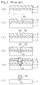
- Figures 2(a) to 2(f) are cross sections illustrating process steps in a method of a T-shaped gate electrode of a prior art semiconductor device.
- reference numeral 1 designates a compound semiconductor substrate
- numeral 1a designates a recess
- numeral 2 designates an insulating film
- numeral 6 designates a gate metal
- numeral 6a designates a T-shaped gate electrode
- numeral 7 designates a photoresist film for electron beam exposure
- numeral 8 designates a photoresist film for optical exposure
- numerals 7a and 8a designate apertures.
- a photoresist for electron beam exposure 7 is successively deposited on a photoresist for optical exposure 8.
- the photoresist for electron beam exposure and the photoresist for optical exposure must not be mixed with each other, namely, resin of the electron beam photoresist must not be dissolved by solvent of the optical photoresist. Therefore, photoresists comprising resin and solvent satisfying the above-described condition, are selected as the electron beam photoresist and the optical photoresist.
- a first aperture 8a of a relatively large width is formed in the optical photoresist film 8.
- a second aperture 7a of a relatively small width is formed.
- a recess 1a is formed by etching the compound semiconductor substrate 1.
- a gate metal 6 is deposited on the whole surface of the substrate and lift off is conducted to form a T-shaped gate electrode 6a as illustrated in Figure 2(f).
- the photoresist aperture pattern for prescribing lower part electrode width of the T-shape gate electrode is produced.
- this pattern exposure method employing electron beam irradiation in drawing patterns, it is difficult to enhance throughput in manufacturing semiconductor devices.
- the photoresist aperture pattern for prescribing an upper part electrode width of the T-shaped gate electrode is produced, namely, when the optical photoresist film 8 is developed, it is necessary that the electron beam photoresist film 7 below the photoresist film 8 is not developed by the developer of the film 8.
- the photoresist film 8 is deposited on the photoresist film 7, these films are required not to mix with each other. Therefore, the degree of freedom in selecting materials of photoresist is unfavorably restricted to a great extent.
- the resolution limit is at most 0.2 to 0.25 microns and the gate length is not shortened below such length.
- a gate length is controlled just by adjusting the thickness of the metal film in depositing the metal film, resulting in shortening the gate length easily and efficiently.
- the metal film is easily formed so that its thickness is below 0.2 microns, the gate length is shortened to below 0.2 microns.
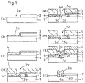
- Figures 1(a) to 1(h) are cross sections illustrating process steps in a method for producing a T-shaped gate electrode in accordance with an embodiment of the present invention.
- Figures 2(a) to 2(f) are cross sections illustrating process steps in a method for producing a prior art T-shaped gate electrode.
- Figures 1(a) to 1(h) are cross sections illustrating process steps in a method for producing a T-shaped gate electrode in accordance with an embodiment of the present invention.
- the same reference numerals as those of Figures 2(a) to 2(f) designate the same or corresponding parts.
- Reference numeral 2 designates an insulating film
- numeral 2a designates an aperture
- numeral 2b designates a sidewall of the insulating film
- numeral 3 designates a WSi (tungsten silicide) film
- numeral 3a designates an aperture
- numeral 3b a WSi film formed along the sidewall 2b of the insulating film
- numeral 3c designates a sidewall of the WSi film 3
- numeral 4 designates a photoresist film
- numeral 4a designates a sidewall of the photoresist film
- numeral 5 designates a photoresist aperture pattern
- numeral 5a designates an aperture.
- an insulating film 2 for example, comprising SiO2 about 5000 ⁇ thick is deposited on the compound semiconductor substrate 1 comprising GaAs or InP with plasma CVD method or the like. And, by etching a prescribed portion of the insulating film 2, an aperture 2a is produced so that its end is disposed in a region where the gate electrode would be produced.
- a WSi film 3 is deposited on the entire surface of the wafer by spattering or CVD method so that its thickness is a little under 0.2 microns.
- a photoresist aperture pattern 5 providing an aperture 5a of a thickness of approximately 1 micron is produced so that a central portion of the aperture 5a for prescribing an upper electrode width of the T-shaped gate electrode which would be formed in a later process, is disposed on a WSi film 3b formed on the sidewall of the aperture 2a, namely, a sidewall 2b of the insulating film 2.
- the recess 1a is formed.
- a gate metal 6 formed by laminating a gold layer on a titanium layer or the like, on the entire surface of the wafer, a T-shaped gate electrode 6a is formed on the bottom surface of the recess 1a. Then, the unnecessary gate metal 6, the photoresist aperture pattern 5 and the photoresist film 4 is removed by lift off.
- the width of the aperture 3a of a mask prescribing the gate length depends on the thickness of the WSi film 3 disposed along the sidewall 2a of the insulating film 2 on the compound semiconductor substrate 1, which becomes a sidewall of the aperture 3a of the mask. Therefore, when the WSi film 3 is deposited on the entire surface of the wafer, just controlling its thickness enables the gate length to be shortened easily. In addition, since the thickness of the WSi film 3 obtained by deposition is reduced to below 0.2 microns, the gate length is shortened to under 0.2 microns.
- the photoresist aperture pattern 5 is formed in a conventional photolithography technique, namely, a photolithography technique including pattern exposure process employing an optical exposure apparatus, and the photoresist film 4 is just employed for a mask in etching the WSi film 3, even if photoresists comprising materials which causes mixing with each other are employed as the photoresists constituting the photoresist film 4 and the photoresist aperture pattern 5, these photoresists do not give bad influences to controllability of forming the electrode. As a result, the degree of freedom in selecting materials of photoresist is enhanced and process steps of producing a gate electrode having little restriction of selection of materials are obtained.
- WSi film 3 is deposited as a metal film, a film comprising other refractory metal can be employed with the same effects as described above.
Landscapes
- Junction Field-Effect Transistors (AREA)
- Electrodes Of Semiconductors (AREA)
Applications Claiming Priority (2)
| Application Number | Priority Date | Filing Date | Title |
|---|---|---|---|
| JP285006/92 | 1992-09-29 | ||
| JP28500692 | 1992-09-29 |
Publications (2)
| Publication Number | Publication Date |
|---|---|
| EP0591608A2 true EP0591608A2 (fr) | 1994-04-13 |
| EP0591608A3 EP0591608A3 (fr) | 1995-01-25 |
Family
ID=17685932
Family Applications (1)
| Application Number | Title | Priority Date | Filing Date |
|---|---|---|---|
| EP93104467A Withdrawn EP0591608A3 (fr) | 1992-09-29 | 1993-03-18 | Méthode de fabrication d'une électrode de porte en forme de T dans un dispositif semi-conducteur. |
Country Status (2)
| Country | Link |
|---|---|
| US (1) | US5304511A (fr) |
| EP (1) | EP0591608A3 (fr) |
Cited By (3)
| Publication number | Priority date | Publication date | Assignee | Title |
|---|---|---|---|---|
| WO2002063671A3 (fr) * | 2001-01-17 | 2002-10-10 | United Monolithic Semiconduct | Procede pour fabriquer un composant semi-conducteur comportant une electrode de contact en forme de t |
| WO2003096399A1 (fr) * | 2002-05-11 | 2003-11-20 | United Monolithic Semiconductors Gmbh | Procede de production d'un composant semi-conducteur et composant semi-conducteur ainsi produit |
| RU2390875C1 (ru) * | 2009-04-13 | 2010-05-27 | Федеральное государственное унитарное предприятие "Научно-производственное предприятие "Исток" (ФГУП НПП "Исток") | Способ изготовления транзистора свч с управляющим электродом т-образной конфигурации субмикронной длины |
Families Citing this family (15)
| Publication number | Priority date | Publication date | Assignee | Title |
|---|---|---|---|---|
| JP2560993B2 (ja) * | 1993-09-07 | 1996-12-04 | 日本電気株式会社 | 化合物半導体装置の製造方法 |
| JP2565119B2 (ja) * | 1993-11-30 | 1996-12-18 | 日本電気株式会社 | パターン形成方法 |
| US5486483A (en) * | 1994-09-27 | 1996-01-23 | Trw Inc. | Method of forming closely spaced metal electrodes in a semiconductor device |
| EP0708481A3 (fr) * | 1994-10-20 | 1997-04-02 | Hughes Aircraft Co | Bosses thermiques améliorées pour circuits intégrés monolithiques de haute puissance du type flip chip et procédé de fabrication |
| DE19509231C2 (de) * | 1995-03-17 | 2000-02-17 | Ibm | Verfahren zum Aufbringen einer Metallisierung auf einem Isolator und zum Öffnen von Durchgangslöchern in diesem |
| KR100228385B1 (ko) * | 1996-12-21 | 1999-11-01 | 정선종 | 반도체 소자의 게이트 전극 제조 방법 |
| US6051454A (en) * | 1997-09-11 | 2000-04-18 | Matsushita Electric Industrial Co., Ltd. | Semiconductor device and method for fabricating the same |
| US5940697A (en) * | 1997-09-30 | 1999-08-17 | Samsung Electronics Co., Ltd. | T-gate MESFET process using dielectric film lift-off technique |
| KR100262940B1 (ko) * | 1998-05-29 | 2000-09-01 | 이계철 | 절연막 리프트 오프를 이용한 화합물 반도체 소자 제조 방법 |
| US6596598B1 (en) | 2000-02-23 | 2003-07-22 | Advanced Micro Devices, Inc. | T-shaped gate device and method for making |
| EP1990833A3 (fr) * | 2000-02-25 | 2010-09-29 | Ibiden Co., Ltd. | Carte de circuit imprimé multicouche et son procédé de fabrication |
| KR20030060898A (ko) * | 2000-09-25 | 2003-07-16 | 이비덴 가부시키가이샤 | 반도체소자,반도체소자의 제조방법,다층프린트배선판 및다층프린트배선판의 제조방법 |
| US20070134943A2 (en) * | 2006-04-02 | 2007-06-14 | Dunnrowicz Clarence J | Subtractive - Additive Edge Defined Lithography |
| US9728444B2 (en) * | 2015-12-31 | 2017-08-08 | International Business Machines Corporation | Reactive ion etching assisted lift-off processes for fabricating thick metallization patterns with tight pitch |
| CN109728086A (zh) * | 2017-10-31 | 2019-05-07 | 中国工程物理研究院电子工程研究所 | 侧墙栅高迁移率晶体管的制备方法 |
Family Cites Families (8)
| Publication number | Priority date | Publication date | Assignee | Title |
|---|---|---|---|---|
| JPS6182482A (ja) * | 1984-09-29 | 1986-04-26 | Toshiba Corp | GaAs電界効果トランジスタの製造方法 |
| JPH01243476A (ja) * | 1988-03-25 | 1989-09-28 | Nec Corp | 電極形成方法 |
| JPH02138750A (ja) * | 1988-08-24 | 1990-05-28 | Mitsubishi Electric Corp | 半導体装置の製造方法 |
| JPH0279437A (ja) * | 1988-09-14 | 1990-03-20 | Mitsubishi Electric Corp | 半導体装置の製造方法 |
| JPH0355852A (ja) * | 1989-07-25 | 1991-03-11 | Sony Corp | 半導体装置の製造方法 |
| JPH03278543A (ja) * | 1990-03-28 | 1991-12-10 | Nec Corp | 電界効果トランジスタの製造方法 |
| JPH03289142A (ja) * | 1990-04-06 | 1991-12-19 | Sumitomo Electric Ind Ltd | 化合物半導体装置の製造方法 |
| US5240878A (en) * | 1991-04-26 | 1993-08-31 | International Business Machines Corporation | Method for forming patterned films on a substrate |
-
1993
- 1993-03-09 US US08/028,115 patent/US5304511A/en not_active Expired - Fee Related
- 1993-03-18 EP EP93104467A patent/EP0591608A3/fr not_active Withdrawn
Cited By (6)
| Publication number | Priority date | Publication date | Assignee | Title |
|---|---|---|---|---|
| WO2002063671A3 (fr) * | 2001-01-17 | 2002-10-10 | United Monolithic Semiconduct | Procede pour fabriquer un composant semi-conducteur comportant une electrode de contact en forme de t |
| US6790717B2 (en) | 2001-01-17 | 2004-09-14 | United Monolithic Semiconductors Gmbh | Method for producing a semiconductor component comprising a t-shaped contact electrode |
| WO2003096399A1 (fr) * | 2002-05-11 | 2003-11-20 | United Monolithic Semiconductors Gmbh | Procede de production d'un composant semi-conducteur et composant semi-conducteur ainsi produit |
| US7041541B2 (en) | 2002-05-11 | 2006-05-09 | United Monolithic Semiconductors Gmbh | Method for producing a semiconductor component, and semiconductor component produced by the same |
| US7432563B2 (en) | 2002-05-11 | 2008-10-07 | United Monolithic Semiconductors Gmbh | Method for producing a semiconductor component and semiconductor component produced by the same |
| RU2390875C1 (ru) * | 2009-04-13 | 2010-05-27 | Федеральное государственное унитарное предприятие "Научно-производственное предприятие "Исток" (ФГУП НПП "Исток") | Способ изготовления транзистора свч с управляющим электродом т-образной конфигурации субмикронной длины |
Also Published As
| Publication number | Publication date |
|---|---|
| EP0591608A3 (fr) | 1995-01-25 |
| US5304511A (en) | 1994-04-19 |
Similar Documents
| Publication | Publication Date | Title |
|---|---|---|
| EP0591608A2 (fr) | Méthode de fabrication d'une électrode de porte en forme de T dans un dispositif semi-conducteur | |
| US5503962A (en) | Chemical-mechanical alignment mark and method of fabrication | |
| US5641610A (en) | Method for producing a multi-step structure in a substrate | |
| US5023203A (en) | Method of patterning fine line width semiconductor topology using a spacer | |
| US4776922A (en) | Formation of variable-width sidewall structures | |
| EP0238690B1 (fr) | Procédé pour la formation de flancs latéraux | |
| EP0470707B1 (fr) | Méthode pour structurer une couche | |
| US4871630A (en) | Mask using lithographic image size reduction | |
| US5670298A (en) | Method of forming a metal pattern in manufacturing a semiconductor device | |
| US6136723A (en) | Dry etching process and a fabrication process of a semiconductor device using such a dry etching process | |
| US5326727A (en) | Method for integrated circuit fabrication including linewidth control during etching | |
| US5041362A (en) | Dry developable resist etch chemistry | |
| US5366849A (en) | Photoresist pattern formation through etching where the imaging exposure changes in a given direction in the desired pattern and inclined vapor deposition is utilized to deposit a film | |
| US4973544A (en) | Method for reversing tone or polarity of pattern on integrated circuit substrate utilizing reverse casting by planarization | |
| EP0178654A2 (fr) | Procédé pour la fabrication d'un dispositif semi-conducteur comportant une méthode pour configurer un matériau organique | |
| WO1983003485A1 (fr) | Procede de formation d'un materiau de protection lithographique hybride a rayon electronique/optique | |
| US5736276A (en) | Method for fabricating phase inverted mask | |
| CA1260627A (fr) | Photomasque de reduction de la taille d'images lithographiques | |
| KR950004974B1 (ko) | 미세패턴 형성방법 | |
| KR910001193B1 (ko) | 반도체 장치의 제조방법 | |
| KR100278742B1 (ko) | 고반사 물질의 미세 패턴 형성 방법 | |
| Nagarajan et al. | Sub-Half Micrometer Gate Lift-Off By Three Layer Resist Process Via Electron Beam Lithography For Gallium Arsenide Monolithic Microwave Integrated Circuits (MIMICs) | |
| KR100248345B1 (ko) | 반도체 소자의 금속 배선 형성 방법 | |
| KR950009293B1 (ko) | 식각선택비가 향상된 단층레지스트 패턴 형성방법 | |
| KR0137573B1 (ko) | 전계효과 트랜지스터의 게이트 형성방법 |
Legal Events
| Date | Code | Title | Description |
|---|---|---|---|
| PUAI | Public reference made under article 153(3) epc to a published international application that has entered the european phase |
Free format text: ORIGINAL CODE: 0009012 |
|
| AK | Designated contracting states |
Kind code of ref document: A2 Designated state(s): DE FR GB |
|
| PUAL | Search report despatched |
Free format text: ORIGINAL CODE: 0009013 |
|
| AK | Designated contracting states |
Kind code of ref document: A3 Designated state(s): DE FR GB |
|
| 17P | Request for examination filed |
Effective date: 19950216 |
|
| 17Q | First examination report despatched |
Effective date: 19951219 |
|
| 18D | Application deemed to be withdrawn |
Effective date: 19960430 |