EP0612112A2 - Chalkopyrit-Halbleiterfilm und Herstellungsverfahren - Google Patents
Chalkopyrit-Halbleiterfilm und Herstellungsverfahren Download PDFInfo
- Publication number
- EP0612112A2 EP0612112A2 EP94102089A EP94102089A EP0612112A2 EP 0612112 A2 EP0612112 A2 EP 0612112A2 EP 94102089 A EP94102089 A EP 94102089A EP 94102089 A EP94102089 A EP 94102089A EP 0612112 A2 EP0612112 A2 EP 0612112A2
- Authority
- EP
- European Patent Office
- Prior art keywords
- film
- group
- chalcopyrite
- iii
- substrate
- Prior art date
- Legal status (The legal status is an assumption and is not a legal conclusion. Google has not performed a legal analysis and makes no representation as to the accuracy of the status listed.)
- Granted
Links
Images




Classifications
-
- H—ELECTRICITY
- H10—SEMICONDUCTOR DEVICES; ELECTRIC SOLID-STATE DEVICES NOT OTHERWISE PROVIDED FOR
- H10F—INORGANIC SEMICONDUCTOR DEVICES SENSITIVE TO INFRARED RADIATION, LIGHT, ELECTROMAGNETIC RADIATION OF SHORTER WAVELENGTH OR CORPUSCULAR RADIATION
- H10F77/00—Constructional details of devices covered by this subclass
- H10F77/10—Semiconductor bodies
- H10F77/12—Active materials
- H10F77/126—Active materials comprising only Group I-III-VI chalcopyrite materials, e.g. CuInSe2, CuGaSe2 or CuInGaSe2 [CIGS]
-
- Y—GENERAL TAGGING OF NEW TECHNOLOGICAL DEVELOPMENTS; GENERAL TAGGING OF CROSS-SECTIONAL TECHNOLOGIES SPANNING OVER SEVERAL SECTIONS OF THE IPC; TECHNICAL SUBJECTS COVERED BY FORMER USPC CROSS-REFERENCE ART COLLECTIONS [XRACs] AND DIGESTS
- Y02—TECHNOLOGIES OR APPLICATIONS FOR MITIGATION OR ADAPTATION AGAINST CLIMATE CHANGE
- Y02E—REDUCTION OF GREENHOUSE GAS [GHG] EMISSIONS, RELATED TO ENERGY GENERATION, TRANSMISSION OR DISTRIBUTION
- Y02E10/00—Energy generation through renewable energy sources
- Y02E10/50—Photovoltaic [PV] energy
- Y02E10/541—CuInSe2 material PV cells
-
- Y—GENERAL TAGGING OF NEW TECHNOLOGICAL DEVELOPMENTS; GENERAL TAGGING OF CROSS-SECTIONAL TECHNOLOGIES SPANNING OVER SEVERAL SECTIONS OF THE IPC; TECHNICAL SUBJECTS COVERED BY FORMER USPC CROSS-REFERENCE ART COLLECTIONS [XRACs] AND DIGESTS
- Y02—TECHNOLOGIES OR APPLICATIONS FOR MITIGATION OR ADAPTATION AGAINST CLIMATE CHANGE
- Y02P—CLIMATE CHANGE MITIGATION TECHNOLOGIES IN THE PRODUCTION OR PROCESSING OF GOODS
- Y02P70/00—Climate change mitigation technologies in the production process for final industrial or consumer products
- Y02P70/50—Manufacturing or production processes characterised by the final manufactured product
-
- Y—GENERAL TAGGING OF NEW TECHNOLOGICAL DEVELOPMENTS; GENERAL TAGGING OF CROSS-SECTIONAL TECHNOLOGIES SPANNING OVER SEVERAL SECTIONS OF THE IPC; TECHNICAL SUBJECTS COVERED BY FORMER USPC CROSS-REFERENCE ART COLLECTIONS [XRACs] AND DIGESTS
- Y10—TECHNICAL SUBJECTS COVERED BY FORMER USPC
- Y10S—TECHNICAL SUBJECTS COVERED BY FORMER USPC CROSS-REFERENCE ART COLLECTIONS [XRACs] AND DIGESTS
- Y10S148/00—Metal treatment
- Y10S148/153—Solar cells-implantations-laser beam
-
- Y—GENERAL TAGGING OF NEW TECHNOLOGICAL DEVELOPMENTS; GENERAL TAGGING OF CROSS-SECTIONAL TECHNOLOGIES SPANNING OVER SEVERAL SECTIONS OF THE IPC; TECHNICAL SUBJECTS COVERED BY FORMER USPC CROSS-REFERENCE ART COLLECTIONS [XRACs] AND DIGESTS
- Y10—TECHNICAL SUBJECTS COVERED BY FORMER USPC
- Y10S—TECHNICAL SUBJECTS COVERED BY FORMER USPC CROSS-REFERENCE ART COLLECTIONS [XRACs] AND DIGESTS
- Y10S438/00—Semiconductor device manufacturing: process
- Y10S438/93—Ternary or quaternary semiconductor comprised of elements from three different groups, e.g. I-III-V
Definitions
- the present invention relates to a chalcopyrite structure semiconductor thin film containing a specific dopant and a process of producing the same.
- the chalcopyrite structure semiconductor is a material useful for constituting light-emitting devices and solar cells, because its forbidden band can be wide from a visual region to an infrared ray region and it has a large optical absorption coefficient due to the constituent elements. It is indispensable to produce a p-n junction in manufacturing the solar cells or light-emitting devices.
- a method of changing the composition ratio between a Group I element and a Group III element or between a Group II element and a Group IV element which are the constituent elements of chalcopyrite compounds has been used conventionally.
- n-type is formed when the proportion of the Group III element Cu is less than that of the Group I element In, and in the opposite case p-type is formed.
- such problem is encountered that many lattice defects occur due to deviations in the composition ratio.
- R. Noufi et al. also report that, it is difficult to control a carrier concentration and resistivity by changing the composition ratio (Appl. Phys. Lett., 45 (1984) p.688).
- most of the chalcopyrite semiconductor thin film which takes the n-type by deviation in the composition ratio shows a high resistance, and thus a low resistance film is not obtainable.
- a depletion layer of the p-n junction must be broaden to convert incident light efficiently into electrical energy. Thus it is necessary to control the carrier concentration.
- the present invention provides a chalcopyrite structure semiconductor film comprising a Group I-III-VI 2 chalcopyrite compound containing a Group VII element as a dopant.
- the present invention further relates to a process of producing a chalcopyrite thin film, whereby conventionally problems are solved, constituent element composition is in a stoichiometric ratio and electrical characteristics such as p-n conduction types and carrier concentration are controlled.
- a first process of producing the chalcopyrite structure semiconductor film of the present invention comprises: depositing a I-III-VI 2 chalcopyrite compound film on a substrate while evaporating onto the substrate a Group VII element, to obtain a I-III-VI 2 chalcopyrite compound film containing the Group VII element therein as a dopant.
- a second process of producing the chalcopyrite structure semiconductor film of the present invention comprises the steps of: depositing a I-III-VI 2 chalcopyrite compound film on a substrate, and heat treating the deposited chalcopyrite compound film in an atmosphere containing a vapor of a Group VII element or its compound to obtain a I-III-VI 2 chalcopyrite compound film containing the Group VII element therein as a dopant.
- the process further comprises the step of heat treating the chalcopyrite compound film containing the Group VII element as a dopant, preferably in an atmosphere containing gas selected from the group consisting hydrogen, nitrogen, oxygen, helium and argon.
- the preferable temperature of the heat treating lies in the range of from 200°C to 400°C.
- the process further comprises the step of heat treating the chalcopyrite compound film containing the Group VII element as a dopant in an atmosphere containing a vapor of the Group VI element.
- the heat treating the deposited chalcopyrite compound film in the atmosphere containing the vapor of the Group VII element or its compound is carried out under a vacuum of 10 ⁇ 9 Torr to 10 ⁇ 2 Torr.
- a third process of producing the chalcopyrite structure semiconductor film of the present invention comprises the steps of: depositing a I-III-VI 2 chalcopyrite compound film on a substrate, and heat treating the deposited chalcopyrite compound film in an atmosphere containing a gaseous compound of a Group VII element to obtain a chalcopyrite compound film containing the Group VII element therein as a dopant.
- a fourth process of producing the chalcopyrite semiconductor film of the present invention comprises the steps of: depositing a film comprising a Group I element and a Group III element on a substrate, and heat treating the film in an atmosphere containing a vapor of a Group VI element or its gaseous compound and a gaseous compound of a Group VII element to obtain a I-III-VI 2 chalcopyrite compound containing the Group VII element as a dopant.
- the present invention further provides a solar cell whose absorber layer or heterojunction forming layer comprises a I-III-VI 2 chalcopyrite semiconductor film containing a Group VII element as a dopant.
- the present invention also provides a light-emitting device whose active layer or clad layer comprises a I-III-VI 2 chalcopyrite semiconductor film containing a Group VII element as a dopant.
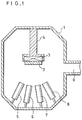
- FIG.1 is a longitudinal sectional view showing a schematic configuration of an apparatus for obtaining a I-III-VI 2 chalcopyrite structure semiconductor thin film doped with a Group VII element in one embodiment of the present invention.
- FIG.2 shows the relationship between a substrate temperature, a InCl3 crucible temperature and resistivity of a CIS:Cl film obtained in embodiment 1 of the present invention.
- FIG.3 shows the relationship between a substrate temperature, a InCl3 crucible temperature at the time of heat treating a CIS film and resistivity of a resultant CIS:Cl film in embodiment 2.
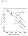
- FIG.4 shows the relationship between a HCl content in an atmosphere, a heat treatment temperature at the time of heat treating a CIS film and resistivity of a resultant CIS:Cl film in embodiment 3.
- FIG.5 shows distributions of Cl element in a CIS:Cl film obtained in embodiments 1 to 4.
- FIG.6 shows the relationship between a HCl content in an atmosphere at the time of obtaining the CIS:Cl film and resistivity of a resultant CIS:Cl film in embodiments 5 and 6.
- FIG.7 is a longitudinal sectional view showing an example of configuration of a solar cell device using a I-III-VI 2 film according to the present invention.
- FIG.8 shows a band configuration of the device.
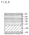
- FIG.9 is a longitudinal sectional view showing an example of configuration of a light-emitting device using a I-III-VI 2 film according to the present invention.
- the present invention is directed to a Group I-III-VI 2 chalcopyrite structure semiconductor film containing a Group VII element as a dopant, and to methods for producing the same.
- the I-III-VI 2 chalcopyrite structure semiconductor thin film of the present invention is that, by containing the Group VII element as a dopant, the composition of constituent elements is in a stoichiometric ratio, and electrical characteristics such as p-n conduction types and carrier concentration are controlled.
- the Group VI element in the deposited chalcopyrite structure is partly substituted by the Group VII element.
- the second or third production process of the present invention by heat treating the deposited I-III-VI 2 thin film in an atmosphere containing a vapor of the Group VII element or its compound, or an atmosphere containing a gaseous compound of the Group VII element under a vacuum or a gas atmosphere, the Group VI element in the I-III-VI 2 chalcopyrite is substituted by the Group VII element (hereinafter, the second and the third production processes are referred to as "diffusion process").
- the fourth production process of the present invention by heat treating a film comprising the Group I and Group III elements in an atmosphere containing a vapor of the Group VI element or its gaseous compound and a gaseous compound of the Group VII element, the Group VII element is taken into the resultant I-III-VI 2 chalcopyrite film, and the Group VI element in the film is partly substituted by the Group VII element.
- the I-III-VI 2 chalcopyrite structure semiconductor thin film obtained by the present invention becomes a semiconductor film showing an n-type conduction in the presence of excessive electrons caused by partial substitution of the Group VI element by the Group VII element.
- a ratio of the element (dopant) substituted partly as aforementioned against the main element is very small, usually 0.1 atomic % or less, and therefore, the composition ratio of the resultant chalcopyrite thin film can be kept in a stoichiometric ratio.
- the composition ratio of the resultant chalcopyrite thin film can be kept in a stoichiometric ratio.
- a carrier concentration or resistivity of the resultant film can be controlled.
- a degree of freedom on designing the solar cells or light-emitting devices increases, and the desired carrier concentrations or the like necessary for the devices can be obtained easily.
- the substitution takes place from the surface of the chalcopyrite thin film when substituting the dopant and the main element by using the diffusion process, the Group VII element tends to concentrate near the surface, and the concentration inside the film becomes gradually thinner as depth increases.
- an internal electric field is produced in the n-type semiconductor film, and minority carriers (in this case, positive holes) produced near the surface are accelerated inwardly or to the p-n junction interface from the film surface. Therefore, carrier recouplings in the n-type film decrease and a large amount of electric current can be obtained.
- the heat treatment of the n-type chalcopyrite thin film obtained by the aforementioned process an activation factor of the dopant being substituted (an amount of applied electron against an amount of dopant being substituted) can be improved. That is, a low resistance n-type film can be obtained with a little amount of dopant, and deterioration of crystalline quality such as disturbance of the chalcopyrite structure due to excessive impurities is eliminated.
- the n-type chalcopyrite film formed by the diffusion process can be used in a process of optimizing the efficiency of devices such as the solar cells, because a distribution form of the dopant can be controlled by the heat treatment temperature and time.
- the carrier recoupling center decreases, and thus it can realize solar cells having a high conversion efficiency and the light-emitting devices having a high luminous efficiency.
- the range of appropriate temperature for heat treatment in the third process or the fourth process of producing the chalcopyrite structure semiconductor film is between 300 °C and 600 °C.
- the temperature of heat treatment for the chalcopyrite structure films may differ depending on their constituent elements, a film of high quality is not expected to be obtained with heat treatment at a temperature lower than 300 °C.
- the film composition changes owing to desorption of a Group VI element, or Group III and VI elements from a film.
- the Group I element which is applicable to the present invention is, for instance, Cu or Ag.
- the Group III element which is applicable to the present invention is, for instance, Al, Ga or In.
- the Group VI element which is applicable to the present invention is, for instance, S, Se or Te. Further, as the gaseous compound of the Group VI element which is applicable to the present invention, for instance, H2S, CS2, H2Se, (CH3)2Se, (C2H5)2Se or the like may be exemplified.
- the Group VII element which is applicable to the present invention is, for instance, F, Cl or Br. Further, as the gaseous compound of the Group VII element, for instance, HCl, HF or the like may be exemplified.
- FIG.1 shows a schematic configuration of an apparatus for obtaining a chalcopyrite structure semiconductor thin film.
- a support 4 is disposed holding a substrate 2 for depositing a chalcopyrite thin film thereon and including heater 3 for heating the substrate 2.
- a source 5 of Cu, a source 6 of In and a source 7 of Se, which are main constituent elements of chalcopyrite compound CuInSe2, and a source 8 of a dopant including InCl3 are provided.
- An opening 9 is connected to an exhaust system.
- Source crucibles of Cu, In and Se were heated in vacuum of about 10 ⁇ 7 Torr respectively at 1140°C, 860°C and 200°C to evaporate the elements, and simultaneously, Cl was evaporated from the source of InCl3 to deposit a CuInSe2:Cl (CIS:Cl) film on the substrate.
- this production process is referred to as "simultaneous evaporating process”.
- InCl3 when InCl3 is heated, InCl3 is decomposed and only Cl is evaporated at the temperature of about 300°C or less.
- a glass plate partly covered by a ZnO film and an Au film was used as the substrate.
- FIG.2 shows the relationship between the substrate temperature during film forming, InCl3 crucible temperature and resistivity of the resultant CIS:Cl film.
- the resistivity of the resultant film was 104 ⁇ cm or more. Since the resistivity of a CuInSe2 (CIS) film of stoichiometric composition ratio without Cl is about 105 to 104 ⁇ cm, when forming the film at the substrate temperature of 500°C it is understood that Cl hardly goes into the film.
- the film resistivity drops to 103 ⁇ cm when the InCl3 crucible temperature is kept at 300°C. On the contrary, when forming the film at the substrate temperature of 300°C, the film resistivity drops abruptly as the InCl3 crucible temperature rises.
- the chalcopyrite structure is formed not only in the case of substrate temperature of 400°C or higher, but even in the case of substrate temperature of 300°C, when forming the film on a ZnO film.
- the preferable substrate is of a material having polycrystal structure, and amorphous materials or metals are not suitable.
- a semiconductor of a Group VI, e.g., Si, a Group III-VI compound, e.g., CdS or an oxide, e.g., ITO (indium tin oxide), SnO2 or Al2O3 is suitable for the substrate.
- Cu, In and Se are heated to the same temperature as the aforementioned embodiment to produce a CIS film at the substrate temperature of 500°C. Then, the substrate temperature is fixed within a range of 200 to 400°C while evaporating InCl3 from the source in vacuum about 10 ⁇ 7 Torr to heat the CIS film.
- FIG.3 shows the relationship between the substrate temperature, InCl3 crucible temperature and resistivity of the heat treated film.
- the heat treatment time is fixed at 30 minutes.
- Compositions of all of the heat treated films substantially satisfy the stoichiometric composition ratio, and show the n-type conduction.
- the substrate temperature is 200°C
- the change of film resistivity is little against changes in the InCl3 crucible temperatures, and at the InCl3 crucible temperature of 150°C it is not so much different from the resistivity of about 104 ⁇ cm of the CIS film without Cl.
- the resistivity drops abruptly as the InCl3 crucible temperature rises, and at the InCl3 crucible temperature of 300°C, the resistivity drops to about 10 ⁇ cm. This value is lower by three digits than the resistivity of the CIS film without Cl. From this fact, it is understood that the resistivity can be controlled by the InCl3 crucible temperature.
- the temperature range of the substrate for rendering favorable results is 300 °C to 500 °C.
- the CIS film produced at the substrate temperature of 500°C by the same process as the aforementioned embodiment was fed into a quartz tube, and heated while mixed gas of HCl and N2 was being introduced to the quartz tube.
- a flow rate of the mixed gas was 200ml/min., and the heat treatment time was one hour.
- FIG.4 shows the relationship between the HCl gas content in the mixed gas, heat treatment temperature and resistivity of the heat treated CIS film.
- all of the resultant films show n-type.
- the film resistivity drops as the heat treatment temperature rises. Particularly, when the HCl content is 10 vol.% and the heat treatment temperature is 400°C, the film resistivity drops to about 10 ⁇ 2 ⁇ cm.
- FIG.5 shows results of testing distributions of Cl elements in the CIS:Cl film produced in the aforementioned embodiments by a secondary ion mass analysis.
- a curve “a” shows the Cl distribution of the CIS:Cl film produced by the simultaneous evaporating process
- a curve "b” shows that by the vapor-phase diffusion process
- a curve "c” shows that by the gas heat treatment process.
- a curve "d” is to be described later.
- the film produced at the substrate temperature of 400°C or higher has no change in resistivity before and after the after heat treatment.
- the resistivity of the film produced at the substrate temperature of 300°C and InCl3 crucible temperature of 200°C or higher is lower than those before the after heat treatment by one digit. This reason is believed that, substitution takes place from dislocated Cl having entered between lattices to Se forming the crystal structure, and an amount of Cl supplying electrons has increased (increase in activation rate).
- the resistivity of the film heated at the substrate temperature of 200°C increased by the after heat treatment, and the resistivity of the film heated at 300°C or higher decreased by about one digit.
- the chalcopyrite compound film is deposited by three-source evaporation in the above-mentioned embodiments, another preferable deposition method, for example, sputtering or selenization of Cu/In layers in H2Se atmosphere may be employed in the present invention.
- the appropriate temperature for heat treatment is between 200 °C and 600 °C.
- the heat treating time even at the lowest temperature is shorter than 5 hours. As the temperature increases, the treating time becomes shorter. As stated above, such after heat treatment will render activation of the dopant or controlled distribution of the dopant.
- a production process will be described for the fifth embodiment wherein a laminated film of Group I element and Group III element, or a thin film containing the Group I element and Group III element is heated in an atmosphere, containing a gaseous compound of the Group VII element and a vapor of Group VI element.
- this process is referred to as "solid-phase selenization process”.
- a Cu film was deposited by sputtering on a glass substrate at the thickness of about 0.2 ⁇ m. Then, an In film was deposited on the Cu film by sputtering at the thickness of about 0.45 ⁇ m.
- the laminated film and Se powder are fed into a quartz tube, into which mixed gas of HCl gas and N2 gas is introduced to produce a CIS film by heating with a heater provided to produce a CIS film by heating with a heater provided around the quartz tube.
- the curve "d" in FIG.6 shows the relationship between the HCl gas content in the mixed gas and the resistivity of the resultant CIS film.
- the heat treatment temperature is 450°C and the time is 4 hours.
- the resistivity of the film decreases as the HCl gas content increases. This is believed that, as the heat treatment temperature rises, an amount of Cl taken into the film increases and the Cl in the film is activated. Thereby, it is understood that the resistivity can be controlled by the HCl gas content.
- a production process whereby a laminated film of the Group I element and Group III element or a thin film containing the Group I element and group III element is heated in an atmosphere containing a gaseous compound of the Group VI element and a gaseous compound of the Group VII element, is described.
- this process is referred to as "vapor-phase selenization process”.
- Cu and In are deposited simultaneously on a glass substrate to produce a mixed Cu-In film or Cu-In alloy film.
- Composition ratio of Cu and In of the film is about 1:1.
- the mixed film was fed into a quartz tube and heat treated in mixed gas of HCl gas, H2Se gas and N2 gas to obtain a CIS film.
- a broken line curve "f" in FIG.6 shows the relationship between the HCl gas content in the mixed gas and the resistivity of the resultant CIS film.
- the ratio of mixed gases except HCl gas is fixed at 10% H2Se and 90% N2.
- the heat treatment temperature is 450°C and the time is 4 hours.
- the film resistivity decreases as the HCl gas content increases.
- a mixed Cu-In film was fed into a quartz tube, into which mixed gas of H2S, HCl and N2 was introduced to produce CuInS2 by heat treatment.
- the heat treatment is performed at 500°C for 4 hours in the mixed gas having a fixed ratio of 10% H2S and 90% N2 except HCl gas.
- the resistivity of the film can be controlled by changing the HCl gas content. In this case, it is confirmed that, a chalcopyrite structure is formed till the HCl gas content reaches 10%.
- Evaporating source crucibles containing Cu, Al, Se and CuCl were respectively heated at 1140°C, 1200°C, 200°C and 400°C; and a CuAlSe2:Cl film was deposited on GaAs crystals having (100) face at the substrate temperature of 600°C.
- the resultant film was n-type and its resistivity was 1 ⁇ cm. Since the CuAlSe2 film obtained without evaporating CuCl was p-type, it is understood that, the conduction type can be controlled by doping Cl. Meanwhile, when this film was heat treated in an Ar atmosphere at 500°C for 3 hours, the film resistivity dropped to 10 ⁇ 2 ⁇ cm.
- FIG.7 shows one embodiment of the solar cell manufactured by using the present invention.
- a p-type CuInSe2 (CIS) thin film 12 is formed in a predetermined area on a Mo thin film 11 deposited on a glass substrate 10.
- a process of producing the p-type CIS film 12 a process of depositing the 2-layer CIS film having different composition ratios of Cu and In or a process of depositing the CIS film while irradiating a nitrogen ion are suitable.
- vacuum of about 10 ⁇ 7 Torr fixing the substrate temperature of the p-type CIS film at about 300°C, evaporation is carried out for InCl3 and substituting Se by Cl in the CIS film surface to form an n-type CIS:Cl film 13.
- heat treatment is performed in an Ar or N2 atmosphere at 300°C for about 30 minutes.
- Optimum condition of the heat treatment is dependent on an evaporation (, hence substitution) amount of InCl3 and a carrier concentration of the p-type CIS film. Therefore, the atmosphere gas, heat treatment temperature or time are to be selected suitably case by case.
- the heat treatment may sometimes not be necessary depending on the carrier concentration or thickness of the p-type CIS film.
- a ZnO (ZnO:Al) film mixed with 1 wt.% Al is formed as a transparent electrode 14.
- FIG.8 shows a band structure of the device.
- the surface is in an n-type low resistance structure, or a structure wherein a Fermi level is present near a conduction band of the CIS film and gradually approaches to a valence electron band.
- a Fermi level is present near a conduction band of the CIS film and gradually approaches to a valence electron band.
- minority carriers in this case, positive holes
- the resultant current amount increases. Therefore, a high efficiency can be realized.
- an n-type CdS film was deposited by an evaporation method on a high resistance n-type CIS:Cl film formed near the p-type CIS film surface having a reduced Cl doping amount, and a ZnO:Al film was deposited thereon to manufacture the solar cell.
- the internal electric field is produced gently in the whole high-resistance n-type CIS:Cl film disposed between the n-type CdS film and the p-type CIS film. Therefore, the carriers produced in the n-type CIS:Cl layer will be accelerated and taken out from the electrode.
- the carrier recouplings can be reduced, and accordingly the carriers produced by luminous irradiation can be taken out efficiently.
- a higher efficiency of the solar cell is achievable.
- FIG.9 shows one embodiment of a visual range light-emitting device manufactured by using the present invention.
- a low resistance p-type CuAlSe2 film 21 is formed on a GaAs substrate 20, and a high-resistance p-type CuAlSe2 film 22 is formed thereon.
- Cu, Al, Se and CuCl are evaporated simultaneously on the high-resistance p-type CuAlSe2 film 22 to form a high-resistance n-type CuAlSe2:Cl film 23.
- an evaporation amount of CuCl is increased to form a low-resistance n-type CuAlSe2 film 24.
- electrodes 25, 26 consisting of Al or Au are disposed.
- a blue light emission is obtained by injecting the carriers into the p-n junction. At this time, since the carriers are injected from the low- resistance CuAlSe2:Cl film 24, they can be injected efficiently. Thus, a luminous efficiency can be
Landscapes
- Photovoltaic Devices (AREA)
- Physical Deposition Of Substances That Are Components Of Semiconductor Devices (AREA)
- Semiconductor Lasers (AREA)
- Led Devices (AREA)
Priority Applications (1)
| Application Number | Priority Date | Filing Date | Title |
|---|---|---|---|
| EP97113690A EP0817279B1 (de) | 1993-02-15 | 1994-02-10 | Verfahren zur Herstellung von einer Chalcopyrit-Halbleiterdünnschichtstruktur mit einem spezifischen Dotiermaterial |
Applications Claiming Priority (2)
| Application Number | Priority Date | Filing Date | Title |
|---|---|---|---|
| JP2528793A JP3337255B2 (ja) | 1993-02-15 | 1993-02-15 | カルコパイライト構造半導体薄膜とその製造方法、薄膜太陽電池の製造方法、および発光装置の製造方法 |
| JP25287/93 | 1993-02-15 |
Related Child Applications (1)
| Application Number | Title | Priority Date | Filing Date |
|---|---|---|---|
| EP97113690A Division EP0817279B1 (de) | 1993-02-15 | 1994-02-10 | Verfahren zur Herstellung von einer Chalcopyrit-Halbleiterdünnschichtstruktur mit einem spezifischen Dotiermaterial |
Publications (3)
| Publication Number | Publication Date |
|---|---|
| EP0612112A2 true EP0612112A2 (de) | 1994-08-24 |
| EP0612112A3 EP0612112A3 (de) | 1994-12-21 |
| EP0612112B1 EP0612112B1 (de) | 1998-05-13 |
Family
ID=12161808
Family Applications (2)
| Application Number | Title | Priority Date | Filing Date |
|---|---|---|---|
| EP97113690A Expired - Lifetime EP0817279B1 (de) | 1993-02-15 | 1994-02-10 | Verfahren zur Herstellung von einer Chalcopyrit-Halbleiterdünnschichtstruktur mit einem spezifischen Dotiermaterial |
| EP94102089A Expired - Lifetime EP0612112B1 (de) | 1993-02-15 | 1994-02-10 | Verfahren zur Herstellung einer chalkopyrit-Halbleiterschicht |
Family Applications Before (1)
| Application Number | Title | Priority Date | Filing Date |
|---|---|---|---|
| EP97113690A Expired - Lifetime EP0817279B1 (de) | 1993-02-15 | 1994-02-10 | Verfahren zur Herstellung von einer Chalcopyrit-Halbleiterdünnschichtstruktur mit einem spezifischen Dotiermaterial |
Country Status (4)
| Country | Link |
|---|---|
| US (2) | US5389572A (de) |
| EP (2) | EP0817279B1 (de) |
| JP (1) | JP3337255B2 (de) |
| DE (2) | DE69410137T2 (de) |
Families Citing this family (18)
| Publication number | Priority date | Publication date | Assignee | Title |
|---|---|---|---|---|
| DE4442824C1 (de) * | 1994-12-01 | 1996-01-25 | Siemens Ag | Solarzelle mit Chalkopyrit-Absorberschicht |
| EP0743686A3 (de) * | 1995-05-15 | 1998-12-02 | Matsushita Electric Industrial Co., Ltd | Vorprodukt für Halbleiterdünnschichten und Verfahren zur Herstellung von Halbleiterdünnschichten |
| JPH10270733A (ja) * | 1997-01-24 | 1998-10-09 | Asahi Chem Ind Co Ltd | p型半導体、p型半導体の製造方法、光起電力素子、発光素子 |
| DE19723387C2 (de) * | 1997-06-04 | 1999-05-12 | Inst Oberflaechenmodifizierung | Selektives Wasserstoff-Ionenstrahlätzen von binären Fremdphasen in Chalkopyrithalbleiter-Dünnschichten |
| US20100108118A1 (en) * | 2008-06-02 | 2010-05-06 | Daniel Luch | Photovoltaic power farm structure and installation |
| US9865758B2 (en) | 2006-04-13 | 2018-01-09 | Daniel Luch | Collector grid and interconnect structures for photovoltaic arrays and modules |
| US8729385B2 (en) | 2006-04-13 | 2014-05-20 | Daniel Luch | Collector grid and interconnect structures for photovoltaic arrays and modules |
| US9236512B2 (en) | 2006-04-13 | 2016-01-12 | Daniel Luch | Collector grid and interconnect structures for photovoltaic arrays and modules |
| US8884155B2 (en) | 2006-04-13 | 2014-11-11 | Daniel Luch | Collector grid and interconnect structures for photovoltaic arrays and modules |
| EP3327170B1 (de) * | 2007-09-12 | 2020-11-04 | Flisom AG | Vorrichtung zum herstellen eines verbindungsfilms |
| WO2009046178A1 (en) * | 2007-10-02 | 2009-04-09 | University Of Delaware | I-iii-vi2 photovoltaic absorber layers |
| KR101271753B1 (ko) * | 2009-11-20 | 2013-06-05 | 한국전자통신연구원 | 박막형 광 흡수층의 제조 방법, 이를 이용한 박막 태양전지 제조 방법 및 박막 태양전지 |
| WO2011112765A2 (en) | 2010-03-10 | 2011-09-15 | Dow Global Technologies Llc | Flexible solar cell interconnection systems and methods |
| CN102024870B (zh) * | 2010-04-19 | 2013-07-24 | 福建欧德生光电科技有限公司 | 半导体薄膜太阳能电池的制造系统和方法 |
| US8802479B2 (en) | 2010-06-03 | 2014-08-12 | NuvoSun, Inc. | Solar cell interconnection method using a flat metallic mesh |
| BR112014013918A2 (pt) | 2011-12-07 | 2017-06-13 | Nuvosun Inc | método para formar um módulo fotovoltaico, método para formar células fotovoltaicas e célula fotovoltaica |
| RU2567191C1 (ru) * | 2014-07-10 | 2015-11-10 | Федеральное государственное бюджетное учреждение науки Институт проблем химической физики Российской академии наук (ИПХФ РАН) | Способ изготовления фоточувствительных халькопиритных пленок |
| CN111341664B (zh) * | 2020-03-11 | 2022-09-20 | 鄂尔多斯应用技术学院 | 过渡金属元素掺杂CuGaS2的中间带薄膜及其制备方法 |
Family Cites Families (9)
| Publication number | Priority date | Publication date | Assignee | Title |
|---|---|---|---|---|
| US4004342A (en) * | 1976-02-23 | 1977-01-25 | The United States Of America As Represented By The Secretary Of The Air Force | Fabrication of ion implanted P-N junction devices |
| US4311728A (en) * | 1980-10-24 | 1982-01-19 | Exxon Research & Engineering Co. | Method for depositing photoconductive zinc tin phosphide |
| US4915745A (en) * | 1988-09-22 | 1990-04-10 | Atlantic Richfield Company | Thin film solar cell and method of making |
| JPH02270381A (ja) * | 1989-04-11 | 1990-11-05 | Matsushita Electric Ind Co Ltd | 半導体発光素子の製造方法 |
| US5078804A (en) * | 1989-06-27 | 1992-01-07 | The Boeing Company | I-III-VI2 based solar cell utilizing the structure CuInGaSe2 CdZnS/ZnO |
| JPH04324647A (ja) * | 1991-04-24 | 1992-11-13 | Dowa Mining Co Ltd | CuInSe2薄膜の製法 |
| JPH05262504A (ja) * | 1991-09-27 | 1993-10-12 | Matsushita Electric Ind Co Ltd | 化合物半導体、その薄膜製造方法及びそれを用いた半導体装置 |
| EP0534459B1 (de) * | 1991-09-27 | 2000-07-26 | Matsushita Electric Industrial Co., Ltd. | Verfahren zur Herstellung einer Verbindungshalbleiter-Dünnschicht |
| US5286306A (en) * | 1992-02-07 | 1994-02-15 | Shalini Menezes | Thin film photovoltaic cells from I-III-VI-VII compounds |
-
1993
- 1993-02-15 JP JP2528793A patent/JP3337255B2/ja not_active Expired - Lifetime
-
1994
- 1994-02-10 DE DE69410137T patent/DE69410137T2/de not_active Expired - Fee Related
- 1994-02-10 EP EP97113690A patent/EP0817279B1/de not_active Expired - Lifetime
- 1994-02-10 DE DE69431535T patent/DE69431535T2/de not_active Expired - Lifetime
- 1994-02-10 EP EP94102089A patent/EP0612112B1/de not_active Expired - Lifetime
- 1994-02-14 US US08/195,948 patent/US5389572A/en not_active Expired - Fee Related
- 1994-09-30 US US08/316,271 patent/US5474622A/en not_active Expired - Fee Related
Also Published As
| Publication number | Publication date |
|---|---|
| EP0817279A1 (de) | 1998-01-07 |
| DE69431535D1 (de) | 2002-11-14 |
| EP0612112A3 (de) | 1994-12-21 |
| JPH06244442A (ja) | 1994-09-02 |
| US5474622A (en) | 1995-12-12 |
| DE69431535T2 (de) | 2003-06-26 |
| US5389572A (en) | 1995-02-14 |
| DE69410137T2 (de) | 1998-09-03 |
| DE69410137D1 (de) | 1998-06-18 |
| EP0612112B1 (de) | 1998-05-13 |
| EP0817279B1 (de) | 2002-10-09 |
| JP3337255B2 (ja) | 2002-10-21 |
Similar Documents
| Publication | Publication Date | Title |
|---|---|---|
| US5389572A (en) | Process of making chalcopyrite structure semiconductor film | |
| US4523051A (en) | Thin films of mixed metal compounds | |
| EP0853345B1 (de) | Verfahren zur herstellung einer cdte-schicht | |
| EP0206585B1 (de) | Photovoltaische Dünnfilmvorrichtung | |
| US5728231A (en) | Precursor for semiconductor thin films and method for producing semiconductor thin films | |
| KR860001163B1 (ko) | 박막 태양전지 | |
| US8431430B2 (en) | Method for forming a compound semi-conductor thin-film | |
| JP2922466B2 (ja) | 薄膜太陽電池 | |
| US4342879A (en) | Thin film photovoltaic device | |
| JP2922465B2 (ja) | 薄膜太陽電池の製造方法 | |
| JP3311873B2 (ja) | 半導体薄膜の製造方法 | |
| JP3519543B2 (ja) | 半導体薄膜形成用前駆体及び半導体薄膜の製造方法 | |
| JP3337494B2 (ja) | 太陽電池の製造方法及び薄膜太陽電池 | |
| JP3468328B2 (ja) | 半導体薄膜の製造方法 | |
| JPH10150212A (ja) | 半導体薄膜形成用前駆体及び半導体薄膜の製造方法 | |
| JPH05275331A (ja) | カルコパイライト薄膜の製造方法及び太陽電池 | |
| Bhat et al. | Highly uniform, large‐area HgCdTe layers on CdTe and CdTeSe substrates | |
| JPH1088320A (ja) | 半導体薄膜の製造方法 | |
| JP3181074B2 (ja) | Cu系カルコパイライト膜の製造方法 | |
| JP2003179237A (ja) | 半導体薄膜の製造方法および太陽電池 | |
| Bloss et al. | Polycrystalline II-IV-related thin film solar cells | |
| JPH04192373A (ja) | 光起電力素子 | |
| Hill | Cadmium-sulphide/copper-sulphide thin-film solar cells: review of methods of producing the CdS and Cu2S layers | |
| Dimmler et al. | Thin film solar modules based on CIS prepared by the co-evaporation method | |
| Anderson et al. | Cadmium Sulfide/Copper Sulfide Heterojunction Cell Research. Final Report, September 30, 1977-October 31, 1978 |
Legal Events
| Date | Code | Title | Description |
|---|---|---|---|
| PUAI | Public reference made under article 153(3) epc to a published international application that has entered the european phase |
Free format text: ORIGINAL CODE: 0009012 |
|
| 17P | Request for examination filed |
Effective date: 19940210 |
|
| AK | Designated contracting states |
Kind code of ref document: A2 Designated state(s): DE FR GB |
|
| PUAL | Search report despatched |
Free format text: ORIGINAL CODE: 0009013 |
|
| AK | Designated contracting states |
Kind code of ref document: A3 Designated state(s): DE FR GB |
|
| 17Q | First examination report despatched |
Effective date: 19960221 |
|
| GRAG | Despatch of communication of intention to grant |
Free format text: ORIGINAL CODE: EPIDOS AGRA |
|
| GRAG | Despatch of communication of intention to grant |
Free format text: ORIGINAL CODE: EPIDOS AGRA |
|
| GRAH | Despatch of communication of intention to grant a patent |
Free format text: ORIGINAL CODE: EPIDOS IGRA |
|
| GRAH | Despatch of communication of intention to grant a patent |
Free format text: ORIGINAL CODE: EPIDOS IGRA |
|
| GRAA | (expected) grant |
Free format text: ORIGINAL CODE: 0009210 |
|
| DX | Miscellaneous (deleted) | ||
| AK | Designated contracting states |
Kind code of ref document: B1 Designated state(s): DE FR GB |
|
| REF | Corresponds to: |
Ref document number: 69410137 Country of ref document: DE Date of ref document: 19980618 |
|
| ET | Fr: translation filed | ||
| PLBE | No opposition filed within time limit |
Free format text: ORIGINAL CODE: 0009261 |
|
| STAA | Information on the status of an ep patent application or granted ep patent |
Free format text: STATUS: NO OPPOSITION FILED WITHIN TIME LIMIT |
|
| 26N | No opposition filed | ||
| REG | Reference to a national code |
Ref country code: GB Ref legal event code: IF02 |
|
| REG | Reference to a national code |
Ref country code: GB Ref legal event code: 732E |
|
| REG | Reference to a national code |
Ref country code: FR Ref legal event code: TP |
|
| PGFP | Annual fee paid to national office [announced via postgrant information from national office to epo] |
Ref country code: DE Payment date: 20060202 Year of fee payment: 13 |
|
| PGFP | Annual fee paid to national office [announced via postgrant information from national office to epo] |
Ref country code: GB Payment date: 20060208 Year of fee payment: 13 |
|
| PGFP | Annual fee paid to national office [announced via postgrant information from national office to epo] |
Ref country code: FR Payment date: 20060220 Year of fee payment: 13 |
|
| GBPC | Gb: european patent ceased through non-payment of renewal fee |
Effective date: 20070210 |
|
| REG | Reference to a national code |
Ref country code: FR Ref legal event code: ST Effective date: 20071030 |
|
| PG25 | Lapsed in a contracting state [announced via postgrant information from national office to epo] |
Ref country code: DE Free format text: LAPSE BECAUSE OF NON-PAYMENT OF DUE FEES Effective date: 20070901 |
|
| PG25 | Lapsed in a contracting state [announced via postgrant information from national office to epo] |
Ref country code: GB Free format text: LAPSE BECAUSE OF NON-PAYMENT OF DUE FEES Effective date: 20070210 Ref country code: FR Free format text: LAPSE BECAUSE OF NON-PAYMENT OF DUE FEES Effective date: 20070228 |