EP0617457A2 - Verfahren zum Herstellen von Halbleiterscheiben - Google Patents
Verfahren zum Herstellen von Halbleiterscheiben Download PDFInfo
- Publication number
- EP0617457A2 EP0617457A2 EP94302115A EP94302115A EP0617457A2 EP 0617457 A2 EP0617457 A2 EP 0617457A2 EP 94302115 A EP94302115 A EP 94302115A EP 94302115 A EP94302115 A EP 94302115A EP 0617457 A2 EP0617457 A2 EP 0617457A2
- Authority
- EP
- European Patent Office
- Prior art keywords
- wafer
- reverse surface
- polishing
- reverse
- etching
- Prior art date
- Legal status (The legal status is an assumption and is not a legal conclusion. Google has not performed a legal analysis and makes no representation as to the accuracy of the status listed.)
- Granted
Links
Images




Classifications
-
- H—ELECTRICITY
- H10—SEMICONDUCTOR DEVICES; ELECTRIC SOLID-STATE DEVICES NOT OTHERWISE PROVIDED FOR
- H10P—GENERIC PROCESSES OR APPARATUS FOR THE MANUFACTURE OR TREATMENT OF DEVICES COVERED BY CLASS H10
- H10P90/00—Preparation of wafers not covered by a single main group of this subclass, e.g. wafer reinforcement
- H10P90/12—Preparing bulk and homogeneous wafers
-
- Y—GENERAL TAGGING OF NEW TECHNOLOGICAL DEVELOPMENTS; GENERAL TAGGING OF CROSS-SECTIONAL TECHNOLOGIES SPANNING OVER SEVERAL SECTIONS OF THE IPC; TECHNICAL SUBJECTS COVERED BY FORMER USPC CROSS-REFERENCE ART COLLECTIONS [XRACs] AND DIGESTS
- Y10—TECHNICAL SUBJECTS COVERED BY FORMER USPC
- Y10S—TECHNICAL SUBJECTS COVERED BY FORMER USPC CROSS-REFERENCE ART COLLECTIONS [XRACs] AND DIGESTS
- Y10S148/00—Metal treatment
- Y10S148/138—Roughened surface
-
- Y—GENERAL TAGGING OF NEW TECHNOLOGICAL DEVELOPMENTS; GENERAL TAGGING OF CROSS-SECTIONAL TECHNOLOGIES SPANNING OVER SEVERAL SECTIONS OF THE IPC; TECHNICAL SUBJECTS COVERED BY FORMER USPC CROSS-REFERENCE ART COLLECTIONS [XRACs] AND DIGESTS
- Y10—TECHNICAL SUBJECTS COVERED BY FORMER USPC
- Y10S—TECHNICAL SUBJECTS COVERED BY FORMER USPC CROSS-REFERENCE ART COLLECTIONS [XRACs] AND DIGESTS
- Y10S438/00—Semiconductor device manufacturing: process
- Y10S438/974—Substrate surface preparation
Definitions
- This invention relates to a method for the production of a semiconductor wafer, particularly a single crystal silicon wafer (hereinafter referred to simply as "wafer” ).
- the method for the production of a wafer comprises a slicing step for slicing a single crystal ingot pulled up by a single crystal pulling device thereby obtaining wafers of the shape of a thin disc, a chamfering step for chamfering the peripheral edge part of the wafer obtained by the slicing step thereby preventing the wafer from cracking or chipping, a lapping step for lapping the chamfered wafer thereby flattening the surface thereof, an etching step for depriving the lapped wafer of residual mechanical strain, a surface-polishing step for polishing one surface of the etched wafer, and a cleaning step for cleaning the polished wafer thereby removing abrasive and foreign matter adhering thereto.
- a mixed acid is generally used as the etchant for the etching step mentioned above.
- a large undulation W1 having a period in the approximate range of 0.5 to 1 mm and a P-V (peak to valley) value in the approximate range of 0.1 to 0.5 ⁇ m, the magnitudes peculiar to the mixed acid, persists on the reverse side of a wafer W which has not undergone the surface polishing mentioned above as illustrated in Fig. 5 (a) (depicting the wafer W in a free state).
- the method of polishing both the obverse and the reverse sides of the wafer W as illustrated in Fig. 6 (a) may be conceived.
- the undulation W1 illustrated in Fig. 5 (a) is absent from the reverse side of the wafer W, the problem mentioned above does not arise even when the reverse side of the wafer W is fastened through aspiration to the chucking plate 10 as illustrated in Fig. 6 (b) at the step of photolithography.
- the wafer W is fastened through aspiration to the chucking plate 10
- This invention produced by an urge to eliminate the problem mentioned above, has for its object the provision of a method for the production of a wafer which permits detection by a sensor, avoids degrading the resolution of exposure at the step of photolithography during the process of manufacture of a device, and improves the yield of the device.
- this invention provides a method for the production of a wafer which comprises a slicing step for slicing a single crystal ingot thereby obtaining wafers of the shape of a thin disc, a chamfering step for chamfering the wafer obtained by the slicing step, a lapping step for imparting a flat surface to the chamfered wafer, an etching step for removing mechanical strain remaining in the lapped wafer, an obverse surface-polishing step for polishing one side of the etched wafer, and a cleaning step for cleaning the polished wafer, which method is characterized by interposing between the etching step and the surface-polishing step a reverse surface-preparing step for preparing the shape of the reverse side of the wafer.
- the combination of the reverse surface-polishing step with the step of etching treatment is employed as the reverse surface-preparing step in the method of this invention, for example, since the undulation formed on the reverse side of the wafer in consequence of the operation of the preceding etching step is removed by the reverse surface-polishing step, the transfer of the undulation on the reverse side of the wafer toward the obverse surface side entailed by the conventional method does not occur any longer when the wafer is fastened through aspiration to the suction disc at the step of photolithography in the manufacture of a device. As a result, the flatness of the obverse surface of the wafer is kept at a high level, the resolution of exposure is kept similarly at a high level, and the yield of device is prevented from decreasing.
- the reverse surface-polishing step in the reverse surface-preparing step polishes the reverse surface of the wafer to such an extent as to remove the undulation of the reverse surface of the wafer without impairing the flatness of the wafer produced by the etching of the preceding step.
- the wafer which has been deprived of the undulation of the reverse surface thereof at the reverse surface-polishing step has the roughness of the reverse surface thereof exalted at the subsequent step of etching treatment.
- the sensor now is capable of detecting the wafer owing to the exalted roughness. Further, since the reverse surface of the wafer absorbs extraneous particles in the valleys of the acquired surface roughness, the extraneous particles accidentally present produce no adverse effects on the obverse surface side of the wafer. For the same reason as given above, the otherwise possible impairment of the yield of device can be prevented.
- the step of etching treatment in the reverse surface-preparing step exalts exclusively the roughness of the reverse surface of the wafer to an extent enough to absorb the extraneous particles without impairing the flatness of the wafer.
- the combination of the aforementioned reverse surface-polishing step with a sandblasting step and a step of etching treatment or the combination of the reverse surface-polishing step with a BHF treatment step to be adopted as the reverse surface-preparing step can be expected to bring about the same effect as described above.
- Fig. 1 is a block diagram illustrating sequentially in the order of the component steps of the method for the production of a wafer as the first embodiment of this invention.
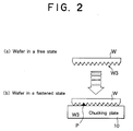
- Fig. 2 (a) is a diagram illustrating a wafer produced by the method of this invention as posed in a free state
- Fig. 2 (b) a diagram illustrating the same wafer in a state fastened through aspiration to a chucking plate.
- Fig. 3 is a block diagram illustrating a main part of the component steps (the part including an added reverse surface-preparing step and the immediately preceding and following steps) of the method for the production of a wafer according to the second embodiment of this invention.
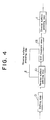
- Fig. 4 is a block diagram illustrating a main part of the component steps (the part including an added reverse surface-preparing step and the immediately preceding and following steps) of the method for the production of a wafer according to the third embodiment of this invention.
- Fig. 5 (a) is a diagram illustrating a wafer produced by the conventional method (the wafer having an undulation on the reverse side) as posed in a free state and Fig. 5 (b) a diagram illustrating the same wafer as fastened through aspiration to a suction disc.
- Fig. 6 (a) is a diagram illustrating a wafer produced by the conventional method (the wafer having polished surfaces on both sides) as posed in a free state and Fig. 6 (b) a diagram illustrating the same wafer as fastened through aspiration to a suction disc.
- Fig. 1 is a block diagram illustrating sequentially in the order of occurrence the component steps of the method for the production of a wafer according to the first embodiment of this invention.
- the method for the production of a wafer according to this invention is characterized by having a reverse surface-preparing step for preparing the shape of the reverse surface of the wafer incorporated in the conventional process between an etching step and an obverse surface-polishing step.
- the present embodiment adopts the combination of a reverse surface-polishing step with a step of etching treatment as the reverse surface-preparing step.
- Fig. 1 illustrates the component steps of the method sequentially in the order of occurrence.
- a single crystal ingot pulled up by a single crystal pulling device not shown is sliced at a right angle or at a certain angle relative to the axial direction of the ingot to obtain a plurality of wafers of the shape of a thin disc.
- the wafer obtained after the slicing step A mentioned above has the peripheral edge part thereof chamfered at a chamfering step B by way of protection against cracking and chipping.
- the chamfered wafer is then lapped with a lapping machine not shown at the next lapping step C.
- the lapped wafer is subjected to an etching treatment with a mixed acid at the subsequent etching step D and is deprived of mechanical strain accumulated throughout the entire obverse surface thereof.
- a large undulation having a period in the approximate range of 0.5 to 1 mm and a P-V value in the approximate range of 0.1 to 0.5 ⁇ m, the magnitudes inherent in the mixed acid, is formed on each of the opposite surfaces of the wafer [(Fig. 5 (a)].
- next obverse surface-polishing step F generally polishes only one surface of the wafer, the undulation formed on the obverse surface of the wafer by the operation of the etching step D remains forever and entails such objectionable effects as mentioned above.
- the present embodiment therefore, has the combination of a reverse surface-polishing step E1 with a step E2 of etching treatment as a reverse surface-preparing step E interposed between the aforementioned etching step D and an obverse surface-polishing step F as described above.
- the reverse surface-polishing step E1 is intended to remove the undulation formed on the reverse surface of the wafer by the operation of the preceding etching step D.
- This reverse surface-polishing step E1 therefore, is only required to polish the reverse surface of the wafer to an extent sufficient to remove the undulation on the reverse surface of the wafer without impairing the flatness of the wafer which has been etched at the preceding step D.
- This polishing removes a thickness of the surface in the range of 3 to 5 ⁇ m under a low load, for example.
- the wafer which has been deprived of the undulation by the operation of the reverse surface-preparing step E1 mentioned above has the roughness of the reverse surface thereof exalted at the next step E2 of etching treatment, with the result that a surface W3 vested with a roughness having an amply shorter period than the undulation W1 (in the approximate range of 1 to 10 ⁇ m, for example) and a P-V value in the approximate range of 0.1 to 0.5 ⁇ m is formed on the reverse surface of the wafer W.
- HF 30 to 50% by weight
- HNO3 5 to 20% by weight
- H20 > 40% by weight for example
- the wafer which has the shape of the reverse surface thereof prepared by the reverse surface-preparing step E mentioned above is subjected to the next obverse surface-polishing step F to have the obverse surface thereof polished and made to acquire a mirror finish and is subsequently cleaned at the next cleaning step G for removal of abradant and other foreign matter adhering to the polished surface.
- the series of steps of which the method for the production of a wafer according to the present embodiment is composed have been described above.
- the wafer W which had an undulation formed on the reverse side thereof at the preceding etching step D is deprived of the undulation at the reverse surface-polishing step E1 in the reverse surface-preparing step E and then the wafer W, as illustrated in Fig. 2 (b), is vested on the reverse side thereof with a surface W3 of a short-period roughness without a sacrifice of the flatness at the step E2 of etching treatment as described above.
- the present embodiment unlike the conventional method, perfectly precludes the probability of the extraneous particle P giving rise to a mound in the obverse surface of the wafer W [Fig. 6 (c)], keeps the flatness surface of the wafer W at a high level and the resolution of exposure at the step of photolithography in the manufacture of a device similarly at a high level, and allows the manufacture of the device to proceed at an exalted yield.
- Fig. 3 is a block diagram illustrating a main part of the component steps (the part including an added reverse surface-preparing step and the immediately preceding and following steps ) of the method for the production of a wafer according to the second embodiment. Since the present embodiment shares the same component steps with the conventional method except for the newly incorporated reverse surface-preparing step, the shared steps will be omitted from the following description.
- This embodiment adopts, as the reverse surface-preparing step, the combination of the same reverse surface-polishing step E1 as in the first embodiment described above with a sandblasting step E3 for promoting a preferential etching operation and a step E4 of etching treatment for exalting the roughness of the reverse surface of the wafer by the preferential etching.
- the reverse surface-polishing step E1 mentioned above is similar to that of the first embodiment described above and is intended to remove a long term undulation formed on the reverse surface of a wafer in consequence of the operation of the preceding etching step D.
- the wafer which was deprived of the undulation on the reverse surface thereof by the reverse surface-polishing step E1 described above is vested on the reverse surface thereof with uniform strain by the blasting of the reverse surface with minute solid particles at the next sandblasting step and is subsequently enabled by the preferential etching operation of the next step E4 of etching treatment to increase the roughness of the reverse surface thereof in the same manner as in the first embodiment described above.
- step E4 of etching treatment in the present embodiment since the step E4 of etching treatment in the present embodiment is intended for selectively etching the strain imparted to the reverse surface of the wafer, it performs the etching treatment with an etchant containing for example 0.5% by weight of NaOH (50 to 60 °C ) for a period of about three minutes.
- an etchant containing for example 0.5% by weight of NaOH (50 to 60 °C ) for a period of about three minutes.
- Fig. 4 is a block diagram illustrating a main part of the component steps (the part including the added reverse surface-adjusting step and the immediately preceding and following steps ) of the method for the production of a wafer according to the third embodiment.
- the present embodiment similarly shares the same steps with the conventional method except for the newly incorporated reverse surface-preparing step. The shared steps, therefore, will be omitted from the following description.
- This embodiment adopts as the reverse surface-preparing step the combination of the same reverse surface-polishing step E1 as in the first embodiment described above with a BHF treatment step E5.
- the reverse surface-polishing step E1 mentioned above is similar to that of the first embodiment described above and is intended to remove a long term undulation formed on the reverse side of the wafer by the preceding etching step D.
- the next BHF treatment step E5 performs an etching operation with a BHF liquid (mixture of NH4 OH with HF) for a period in the approximate range of 30 seconds to 10 minutes for example, to roughen the reverse surface of the wafer without a sacrifice of the flatness in the same manner as in the first and second embodiments described above.
- a BHF liquid mixture of NH4 OH with HF
- the same effect as that of the aforementioned first embodiment is attained because the wafer is deprived of the long term undulation of the reverse surface thereof by the reverse surface-adjusting step E and then is allowed to have the reverse surface thereof roughened to an extent enough to permit discernment of the presence of the wafer by means of a sensor and ensure absorption of an extraneous particle by a valley in the short term undulation.
- the method of this invention for the production of a wafer comprises a slicing step for slicing a single crystal ingot thereby obtaining wafers in the shape of a thin disc, a chamfering step for chamfering the wafer obtained by the slicing step, a lapping step for imparting a flat surface to the chamfered wafer, an etching step for depriving the lapped wafer of mechanical strain, an obverse surface-polishing step for polishing one surface of the etched wafer, and a cleaning step for cleaning the polished wafer and features interposition of a reverse surface-preparing step for preparing the shape of the reverse surface of the wafer between the etching step and the obverse surface-polishing step, it permits production of a wafer which allows manufacture of a device to proceed at an exalted yield by preventing the resolution of exposure at the step of photolithography during the manufacture of the device from being impaired.
Landscapes
- Mechanical Treatment Of Semiconductor (AREA)
Applications Claiming Priority (2)
| Application Number | Priority Date | Filing Date | Title |
|---|---|---|---|
| JP64896/93 | 1993-03-24 | ||
| JP5064896A JP2853506B2 (ja) | 1993-03-24 | 1993-03-24 | ウエーハの製造方法 |
Publications (3)
| Publication Number | Publication Date |
|---|---|
| EP0617457A2 true EP0617457A2 (de) | 1994-09-28 |
| EP0617457A3 EP0617457A3 (de) | 1995-01-11 |
| EP0617457B1 EP0617457B1 (de) | 1998-05-27 |
Family
ID=13271303
Family Applications (1)
| Application Number | Title | Priority Date | Filing Date |
|---|---|---|---|
| EP94302115A Expired - Lifetime EP0617457B1 (de) | 1993-03-24 | 1994-03-24 | Verfahren zum Herstellen von Halbleiterscheiben |
Country Status (4)
| Country | Link |
|---|---|
| US (1) | US5447890A (de) |
| EP (1) | EP0617457B1 (de) |
| JP (1) | JP2853506B2 (de) |
| DE (1) | DE69410514T2 (de) |
Cited By (10)
| Publication number | Priority date | Publication date | Assignee | Title |
|---|---|---|---|---|
| EP0764976A1 (de) * | 1995-08-24 | 1997-03-26 | Shin-Etsu Handotai Company Limited | Methode und Apparatur zur Behandlung von Halbleiter-Wafern |
| EP0798766A1 (de) * | 1996-03-28 | 1997-10-01 | Shin-Etsu Handotai Company Limited | Verfahren zu Herstellung eines monokristallinen Halbleiterwafers mit hochglanzpolierter Oberfläche, unter Benutzung eines Gasphasen-Ätz- und eines Aufwärm-Schrittes, und durch dieses Verfahren hergestellter Wafer |
| EP0791953A3 (de) * | 1996-01-31 | 1998-07-15 | Shin-Etsu Handotai Company Limited | Verfahren zur Herstellung von halbleitenden Scheiben |
| US6114245A (en) * | 1997-08-21 | 2000-09-05 | Memc Electronic Materials, Inc. | Method of processing semiconductor wafers |
| EP0928017A3 (de) * | 1997-12-09 | 2003-07-02 | Shin-Etsu Handotai Company Limited | Herstellungsverfahren für Halbleiterscheiben und danach hergestellte Halbleiterscheiben |
| US7331283B2 (en) | 2004-12-16 | 2008-02-19 | Asml Holding N.V. | Method and apparatus for imprint pattern replication |
| US7363854B2 (en) | 2004-12-16 | 2008-04-29 | Asml Holding N.V. | System and method for patterning both sides of a substrate utilizing imprint lithography |
| US7399422B2 (en) | 2005-11-29 | 2008-07-15 | Asml Holding N.V. | System and method for forming nanodisks used in imprint lithography and nanodisk and memory disk formed thereby |
| US7410591B2 (en) | 2004-12-16 | 2008-08-12 | Asml Holding N.V. | Method and system for making a nano-plate for imprint lithography |
| US7409759B2 (en) | 2004-12-16 | 2008-08-12 | Asml Holding N.V. | Method for making a computer hard drive platen using a nano-plate |
Families Citing this family (20)
| Publication number | Priority date | Publication date | Assignee | Title |
|---|---|---|---|---|
| EP0634658B1 (de) * | 1993-07-16 | 2002-10-16 | Fuji Photo Film Co., Ltd. | Biochemischer Analysator und Inkubator dafür |
| JP3534207B2 (ja) * | 1995-05-16 | 2004-06-07 | コマツ電子金属株式会社 | 半導体ウェーハの製造方法 |
| US6006736A (en) * | 1995-07-12 | 1999-12-28 | Memc Electronic Materials, Inc. | Method and apparatus for washing silicon ingot with water to remove particulate matter |
| JPH0936080A (ja) * | 1995-07-13 | 1997-02-07 | Toray Eng Co Ltd | 加工済シリコンインゴットの洗浄方法 |
| JPH0945643A (ja) * | 1995-07-31 | 1997-02-14 | Komatsu Electron Metals Co Ltd | 半導体ウェハ及びその製造方法 |
| JP3534213B2 (ja) * | 1995-09-30 | 2004-06-07 | コマツ電子金属株式会社 | 半導体ウェハの製造方法 |
| JP3317330B2 (ja) * | 1995-12-27 | 2002-08-26 | 信越半導体株式会社 | 半導体鏡面ウェーハの製造方法 |
| US5821166A (en) * | 1996-12-12 | 1998-10-13 | Komatsu Electronic Metals Co., Ltd. | Method of manufacturing semiconductor wafers |
| JP3620683B2 (ja) * | 1996-12-27 | 2005-02-16 | 信越半導体株式会社 | 半導体ウエーハの製造方法 |
| CN1114566C (zh) * | 1997-06-13 | 2003-07-16 | Cfmt公司 | 处理半导体晶片的方法 |
| JP3358549B2 (ja) | 1998-07-08 | 2002-12-24 | 信越半導体株式会社 | 半導体ウエーハの製造方法ならびにウエーハチャック |
| US6214704B1 (en) | 1998-12-16 | 2001-04-10 | Memc Electronic Materials, Inc. | Method of processing semiconductor wafers to build in back surface damage |
| JP2001096455A (ja) * | 1999-09-28 | 2001-04-10 | Ebara Corp | 研磨装置 |
| US6514423B1 (en) | 2000-02-22 | 2003-02-04 | Memc Electronic Materials, Inc. | Method for wafer processing |
| KR20020034475A (ko) * | 2000-11-02 | 2002-05-09 | 이 창 세 | 반도체급 웨이퍼 제조방법 |
| JP2005039155A (ja) * | 2003-07-18 | 2005-02-10 | Matsushita Electric Ind Co Ltd | 半導体装置の製造方法及びそれに用いる半導体基板の製造方法 |
| JP5368000B2 (ja) * | 2008-04-01 | 2013-12-11 | 信越化学工業株式会社 | Soi基板の製造方法 |
| JP6191154B2 (ja) * | 2013-02-19 | 2017-09-06 | 信越化学工業株式会社 | Soi基板の製造方法 |
| US9281251B2 (en) * | 2013-08-09 | 2016-03-08 | Tokyo Electron Limited | Substrate backside texturing |
| JP7814874B2 (ja) * | 2021-09-24 | 2026-02-17 | 株式会社Screenホールディングス | 研磨方法および基板処理装置 |
Family Cites Families (6)
| Publication number | Priority date | Publication date | Assignee | Title |
|---|---|---|---|---|
| JPS54110783A (en) * | 1978-02-20 | 1979-08-30 | Hitachi Ltd | Semiconductor substrate and its manufacture |
| JPS5958827A (ja) * | 1982-09-28 | 1984-04-04 | Toshiba Corp | 半導体ウエ−ハ、半導体ウエ−ハの製造方法及び半導体ウエ−ハの製造装置 |
| JPS63293813A (ja) * | 1987-05-27 | 1988-11-30 | Hitachi Ltd | 半導体基板 |
| JP2747516B2 (ja) * | 1987-05-31 | 1998-05-06 | 住友シチックス株式会社 | 半導体基板のバックサイドダメージ加工法 |
| JPH0637025B2 (ja) * | 1987-09-14 | 1994-05-18 | スピードファム株式会社 | ウエハの鏡面加工装置 |
| JPH06103678B2 (ja) * | 1987-11-28 | 1994-12-14 | 株式会社東芝 | 半導体基板の加工方法 |
-
1993
- 1993-03-24 JP JP5064896A patent/JP2853506B2/ja not_active Expired - Fee Related
-
1994
- 1994-03-21 US US08/210,437 patent/US5447890A/en not_active Expired - Fee Related
- 1994-03-24 EP EP94302115A patent/EP0617457B1/de not_active Expired - Lifetime
- 1994-03-24 DE DE69410514T patent/DE69410514T2/de not_active Expired - Fee Related
Cited By (15)
| Publication number | Priority date | Publication date | Assignee | Title |
|---|---|---|---|---|
| EP0764976A1 (de) * | 1995-08-24 | 1997-03-26 | Shin-Etsu Handotai Company Limited | Methode und Apparatur zur Behandlung von Halbleiter-Wafern |
| US5882539A (en) * | 1995-08-24 | 1999-03-16 | Shin-Etsu Handotai Co., Ltd. | Wafer processing method and equipment therefor |
| EP0791953A3 (de) * | 1996-01-31 | 1998-07-15 | Shin-Etsu Handotai Company Limited | Verfahren zur Herstellung von halbleitenden Scheiben |
| EP0798766A1 (de) * | 1996-03-28 | 1997-10-01 | Shin-Etsu Handotai Company Limited | Verfahren zu Herstellung eines monokristallinen Halbleiterwafers mit hochglanzpolierter Oberfläche, unter Benutzung eines Gasphasen-Ätz- und eines Aufwärm-Schrittes, und durch dieses Verfahren hergestellter Wafer |
| US5981392A (en) * | 1996-03-28 | 1999-11-09 | Shin-Etsu Handotai Co., Ltd. | Method of manufacturing semiconductor monocrystalline mirror-surface wafers which includes a gas phase etching process, and semiconductor monocrystalline mirror-surface wafers manufactured by the method |
| US6114245A (en) * | 1997-08-21 | 2000-09-05 | Memc Electronic Materials, Inc. | Method of processing semiconductor wafers |
| EP0928017A3 (de) * | 1997-12-09 | 2003-07-02 | Shin-Etsu Handotai Company Limited | Herstellungsverfahren für Halbleiterscheiben und danach hergestellte Halbleiterscheiben |
| EP1564796A1 (de) * | 1997-12-09 | 2005-08-17 | Shin-Etsu Handotai Company Limited | Herstellungsverfahren für Halbleiterscheiben und danach hergestellte Halbleiterscheiben |
| US7331283B2 (en) | 2004-12-16 | 2008-02-19 | Asml Holding N.V. | Method and apparatus for imprint pattern replication |
| US7363854B2 (en) | 2004-12-16 | 2008-04-29 | Asml Holding N.V. | System and method for patterning both sides of a substrate utilizing imprint lithography |
| US7410591B2 (en) | 2004-12-16 | 2008-08-12 | Asml Holding N.V. | Method and system for making a nano-plate for imprint lithography |
| US7409759B2 (en) | 2004-12-16 | 2008-08-12 | Asml Holding N.V. | Method for making a computer hard drive platen using a nano-plate |
| US7882780B2 (en) | 2004-12-16 | 2011-02-08 | Asml Holding N.V. | System and method for patterning both sides of a substrate utilizing imprint lithography |
| US7399422B2 (en) | 2005-11-29 | 2008-07-15 | Asml Holding N.V. | System and method for forming nanodisks used in imprint lithography and nanodisk and memory disk formed thereby |
| US7701668B2 (en) | 2005-11-29 | 2010-04-20 | Asml Holding Nv | System and method for forming nanodisks used in imprint lithography and nanodisk and memory disk formed thereby |
Also Published As
| Publication number | Publication date |
|---|---|
| US5447890A (en) | 1995-09-05 |
| EP0617457B1 (de) | 1998-05-27 |
| DE69410514T2 (de) | 1999-03-04 |
| DE69410514D1 (de) | 1998-07-02 |
| JPH06275480A (ja) | 1994-09-30 |
| JP2853506B2 (ja) | 1999-02-03 |
| EP0617457A3 (de) | 1995-01-11 |
Similar Documents
| Publication | Publication Date | Title |
|---|---|---|
| EP0617457B1 (de) | Verfahren zum Herstellen von Halbleiterscheiben | |
| TW308561B (de) | ||
| EP0774776B1 (de) | Verfahren zur Rückgewinnung von Substraten | |
| JPH06349795A (ja) | 半導体ウエーハの製造方法 | |
| EP1049145A1 (de) | Halbleiterscheibe und herstellungsmethode | |
| US20050148181A1 (en) | Method for producing a silicon wafer | |
| EP1005069A2 (de) | Halbleiterscheibe und Verfahren zu ihrer Herstellung | |
| EP0850724B1 (de) | Oberflächen-Schleifvorrichtung und Verfahren zum oberflächlichen Schleifen eines dünn-flächigen Werkstückes | |
| JP3658454B2 (ja) | 半導体ウェハの製造方法 | |
| US5851924A (en) | Method for fabricating semiconductor wafers | |
| JP2003282491A5 (de) | ||
| US6753256B2 (en) | Method of manufacturing semiconductor wafer | |
| JP2000031099A (ja) | 半導体ウエーハの製造方法 | |
| EP1145296B1 (de) | Herstellungsverfahren einer halbleiterscheibe | |
| US6599760B2 (en) | Epitaxial semiconductor wafer manufacturing method | |
| JP3134719B2 (ja) | 半導体ウェーハ研磨用研磨剤及び研磨方法 | |
| JP2001156030A (ja) | 半導体ウェーハ用研磨ローラおよびこれを用いた半導体ウェーハの研磨方法 | |
| JP2003177100A (ja) | 鏡面面取りウェーハの品質評価方法 | |
| JP3528166B2 (ja) | 高平坦度ウェーハの製造方法 | |
| JP3109419B2 (ja) | ウェーハの加工方法 | |
| JP3551300B2 (ja) | 高平坦度ウェーハの製造方法 | |
| JP2000340571A (ja) | 高平坦度ウェーハの製造方法 | |
| JP2002025950A (ja) | 半導体ウェーハの製造方法 | |
| JP3596405B2 (ja) | 半導体ウェーハの製造方法 | |
| JP3399179B2 (ja) | ウェーハの加工方法 |
Legal Events
| Date | Code | Title | Description |
|---|---|---|---|
| PUAI | Public reference made under article 153(3) epc to a published international application that has entered the european phase |
Free format text: ORIGINAL CODE: 0009012 |
|
| AK | Designated contracting states |
Kind code of ref document: A2 Designated state(s): DE FR GB |
|
| RIN1 | Information on inventor provided before grant (corrected) |
Inventor name: KUDO, HIDEO Inventor name: MASUMURA, HISASHI Inventor name: NAKANO, MASAMI Inventor name: SHIMA, SUNAO Inventor name: KATO, TADAHIRO |
|
| PUAL | Search report despatched |
Free format text: ORIGINAL CODE: 0009013 |
|
| AK | Designated contracting states |
Kind code of ref document: A3 Designated state(s): DE FR GB |
|
| 17P | Request for examination filed |
Effective date: 19941228 |
|
| 17Q | First examination report despatched |
Effective date: 19960711 |
|
| GRAG | Despatch of communication of intention to grant |
Free format text: ORIGINAL CODE: EPIDOS AGRA |
|
| GRAG | Despatch of communication of intention to grant |
Free format text: ORIGINAL CODE: EPIDOS AGRA |
|
| GRAH | Despatch of communication of intention to grant a patent |
Free format text: ORIGINAL CODE: EPIDOS IGRA |
|
| GRAH | Despatch of communication of intention to grant a patent |
Free format text: ORIGINAL CODE: EPIDOS IGRA |
|
| GRAA | (expected) grant |
Free format text: ORIGINAL CODE: 0009210 |
|
| AK | Designated contracting states |
Kind code of ref document: B1 Designated state(s): DE FR GB |
|
| REF | Corresponds to: |
Ref document number: 69410514 Country of ref document: DE Date of ref document: 19980702 |
|
| ET | Fr: translation filed | ||
| PLBE | No opposition filed within time limit |
Free format text: ORIGINAL CODE: 0009261 |
|
| STAA | Information on the status of an ep patent application or granted ep patent |
Free format text: STATUS: NO OPPOSITION FILED WITHIN TIME LIMIT |
|
| PGFP | Annual fee paid to national office [announced via postgrant information from national office to epo] |
Ref country code: GB Payment date: 19990421 Year of fee payment: 6 |
|
| PGFP | Annual fee paid to national office [announced via postgrant information from national office to epo] |
Ref country code: FR Payment date: 19990426 Year of fee payment: 6 |
|
| 26N | No opposition filed | ||
| PG25 | Lapsed in a contracting state [announced via postgrant information from national office to epo] |
Ref country code: GB Free format text: LAPSE BECAUSE OF NON-PAYMENT OF DUE FEES Effective date: 20000324 |
|
| GBPC | Gb: european patent ceased through non-payment of renewal fee |
Effective date: 20000324 |
|
| PG25 | Lapsed in a contracting state [announced via postgrant information from national office to epo] |
Ref country code: FR Free format text: LAPSE BECAUSE OF NON-PAYMENT OF DUE FEES Effective date: 20001130 |
|
| REG | Reference to a national code |
Ref country code: FR Ref legal event code: ST |
|
| PGFP | Annual fee paid to national office [announced via postgrant information from national office to epo] |
Ref country code: DE Payment date: 20030403 Year of fee payment: 10 |
|
| PG25 | Lapsed in a contracting state [announced via postgrant information from national office to epo] |
Ref country code: DE Free format text: LAPSE BECAUSE OF NON-PAYMENT OF DUE FEES Effective date: 20041001 |