EP0649159A1 - Panneau d'affichage à décharge dans un gaz du type courant continu - Google Patents
Panneau d'affichage à décharge dans un gaz du type courant continu Download PDFInfo
- Publication number
- EP0649159A1 EP0649159A1 EP94120109A EP94120109A EP0649159A1 EP 0649159 A1 EP0649159 A1 EP 0649159A1 EP 94120109 A EP94120109 A EP 94120109A EP 94120109 A EP94120109 A EP 94120109A EP 0649159 A1 EP0649159 A1 EP 0649159A1
- Authority
- EP
- European Patent Office
- Prior art keywords
- gas
- discharge
- display panel
- conductive lines
- dce
- Prior art date
- Legal status (The legal status is an assumption and is not a legal conclusion. Google has not performed a legal analysis and makes no representation as to the accuracy of the status listed.)
- Granted
Links
Images


Classifications
-
- H—ELECTRICITY
- H01—ELECTRIC ELEMENTS
- H01J—ELECTRIC DISCHARGE TUBES OR DISCHARGE LAMPS
- H01J17/00—Gas-filled discharge tubes with solid cathode
- H01J17/38—Cold-cathode tubes
- H01J17/48—Cold-cathode tubes with more than one cathode or anode, e.g. sequence-discharge tube, counting tube, dekatron
- H01J17/49—Display panels, e.g. with crossed electrodes, e.g. making use of direct current
- H01J17/492—Display panels, e.g. with crossed electrodes, e.g. making use of direct current with crossed electrodes
-
- H—ELECTRICITY
- H01—ELECTRIC ELEMENTS
- H01J—ELECTRIC DISCHARGE TUBES OR DISCHARGE LAMPS
- H01J17/00—Gas-filled discharge tubes with solid cathode
- H01J17/02—Details
- H01J17/20—Selection of substances for gas fillings; Specified operating pressures or temperatures
Definitions
- the present invention relates to a DC type gas-discharge display panel and a gas-discharge display apparatus using the DC type gas-discharge display panel.
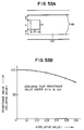
- a first conventional DC type gas-discharge panel has structure thereof as shown in Figs. 1A and 1B.
- Fig. 1A is a sectional view of this first conventional gas-discharge panel
- Fig. 1B is a plan view thereof, as viewed from a display side.
- symbol “FP” indicates a front plate (glass); symbol “BM”, shows a black grid (black matrix); symbol “BA” is a partition; symbol “A” shows an anode (indium tin oxide); symbol “Ph” denotes phosphor; symbol “Ct' shows a cathode (Ni); symbol “D” indicates a dielectric material; symbol “TN” denotes a third electrode; and symbol “RP” shows a rear plate (glass).
- a detailed explanation of this gas-display panel is described in above-mentioned publication (1).
- the display panel of the X-Y matrix is driven by the 1-line at-a-time drive method, and a relatively large current (about 490 ⁇ A) flows therethrough.
- the light-emission efficiency is 0.025 lm/W (white), which implies a low efficiency, and therefore this display panel is not utilized as a color television receiver panel except for a TV receiver panel for special purposes.
- He partial pressure ratio of 93%) - Kr (5%) - Xe (2%) gas is employed as the filling gas, and total pressure thereof is 53 kPa (400 Torr).
- a second conventional DC type gas-discharge display panel In Fig. 2, there is shown a second conventional DC type gas-discharge display panel. It should be noted that the same reference symbols shown in Figs. 1A and 1B are employed to denote the same constructive elements shown in Fig. 2. There are other reference symbols in which symbol “AA” indicates an auxiliary anode; symbol “R-Ph” shows red phosphor; symbol “G-Ph” indicates green phosphor; symbol “B-Ph” is blue-phosphor; symbol “PS” shows a priming slit; symbol “DC” is a display cell; symbol “W” represents a wall; and symbol “ACE” indicates an auxiliary cell.
- symbol “AA” indicates an auxiliary anode
- symbol “R-Ph” shows red phosphor
- symbol “G-Ph” indicates green phosphor
- symbol “B-Ph” is blue-phosphor
- symbol “PS” shows a priming slit
- symbol “DC” is a display cell
- a third conventional DC type gas-discharge panel In Fig. 3, there is shown a third conventional DC type gas-discharge panel. It should be noted that the same reference symbols shown in Figs. 1A, 1B and 2 are employed to denote the same constructive elements shown in Fig. 3. Of the other reference symbols, symbol “F” indicates a filter; symbol “CB” denotes a cathode bus line; symbol “WB” shows a white back; symbol “AAL” is an auxiliary anode line; and symbol “DAL” denotes a display anode line.
- a detailed description of this third conventional display panel is found in above-mentioned publication (3).
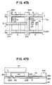
- Figs. 4A and 4B represent a fourth conventional DC type display panel.
- Fig. 4A is a plan view of this display panel, as viewed at a display side
- Fig. 4B is a sectional view thereof cut away along a cutting line X1 - X2 shown in Fig. 4A.
- the structure of this fourth display panel is most similar to that of a DC type gas-discharge display panel according to the present invention.
- the same reference symbols shown in Figs. 1A to 3 are employed to denote the same constructive elements shown in Figs. 4A and 4B.
- reference symbol “AC” denotes an auxiliary cathode
- symbol “DAB” shows a display anode bus line
- symbol “R” indicates a current limiting resistor
- the above-described second to fourth conventional display panels are driven by the pulse memory drive method, the cathodes "C" of which are made of such materials as Ni, Al and LaB6, and in which He-Xe (1.5 to 5%) gas is employed as the filling gas.
- the total pressure of the display panel is from 27 to 33 kPa (200 to 250 Torr).
- peak luminance of an image of the first conventional gas-discharge display panel is about 33 cd/m2, namely dark. Moreover, since the light-emission efficiency is not so high, this first display panel is not adequate to a display panel for a large-screen sized television receiver.
- the practical lifetimes may be predicted as 1,000 hours to 2,000 hours since luminance thereof is increased due to the memory function, and also peak luminance is from 50 to 100 cd/m2. Since when luminance is 100 cd/m2 10,000 hours are required for a practical display, the predicted lifetimes of the second and third conventional display panels constitute a big problem.
- the most important factor determining the lifetime of a display panel is that luminance of this display panel is reduced because sputtered cathode material adheres to the inside of the cells.
- the discharge current can be reduced so as to suppress the sputtering, so that the sustaining discharge currents of the second and third conventional display panels are suppressed to about 100 ⁇ A, but the lifetimes thereof are still short.
- a current limiting resistor is connected to the fourth conventional display tube, so that the sustaining current thereof is lowered and then the lifetime thereof becomes approximately 2 times longer than that of the second or third conventional display panel.
- this longer lifetime is not a practically sufficient lifetime.
- resistors for each of the discharge cells are employed in order to limit the discharge currents flowing through the respective discharge cells.
- This resistor functions to limit the discharge current of the discharge cell to the normal glow discharge region, to dissipate sputtering, and maintain the memory effect in the DC memory type discharge display panel.
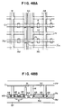
- Figs. 5A and 5B are schematic diagrams of a structure of this discharge display panel.
- Fig. 5A is a plan view of a portion of this discharge panel
- Fig. 5B is a sectional view thereof, taken along a cutting line X3 - X4.
- Fig. 5B is a cutting sectional plane X5 - X6 in Fig. 5B.
- Fig. 1A to 4B are employed to denote the same constructive elements in Figs. 5A and 5B.
- a cathode “C” is formed on a front plate "FP"
- an auxiliary anode “AA” are formed on a rear plate “RP” and positioned perpendicular to the cathode “C”
- a discharge cell “DCE” surrounded by walls “W” are formed on the respective cross points between the anode bus line “AB” and the cathode “C”.
- a resistive material "RM” having an L-shaped form is furthermore fabricated between the anode bus line "AB” and the anode "A”.
- the function of the white glass back "WB” is to electrically insulate the electrode and also to derive the emitted light at the high efficiency.
- a discharge is previously induced between the auxiliary anode “AA” and the cathode “C” so that the commencement of the discharge in the discharge cell is emphasized via the priming slit "PS".
- the L-shaped resistive materials to constitute the resistors have been separately formed with the respective cells.
- a large-sized display panel is manufactured by way of, for instance, the thick-film printing method and the like.
- the conventional panel manufacturing method has a drawback that large fluctuation occurs in the resistance values, depending upon the manufacturing precision, e.g., the dimension and thickness of the resistive materials. Also, the resistance values vary in accordance with the positions and dimensions of the electrodes for terminating this resistor. If the resistance value varies, there are problems that the discharge currents of the respective cells change, and therefore the light-emitting outputs vary, and the variable light appears as fixed pattern noise on a displayed image. In other words, there is a problem that a lack of luminous uniformity, or luminous fluctuation occurs in the respective discharge cells.
- An object of the present invention is to provide a DC type gas-discharge display panel, with low luminous variation in each of discharge cells.
- a DC type gas-discharge display panel comprises: a plurality of discharge cells arranged in a matrix form along a line (row) direction and a column direction; a plurality of resistors provided for each of said discharge cells, for limiting a discharge current of each of said discharge cells; a filling gas filled into each of said discharge cells; a plurality of first conductive lines elongated along the line direction to which one of a desirable discharge controlling potential is applied, each of said first conductive lines being commonly arranged in each of said discharge cells in the respective lines to constitute a first discharge electrode; a plurality of second conductive lines elongated along said column direction, to which the other desirable discharge controlling potential is applied, two adjoining lines of said second conductive lines being commonly arranged with the respective discharge cells; a plurality of second discharge electrodes provided at a substantially central position between each pair of adjoining second conductive lines, which corresponds to each of said discharge cells, for producing a discharge between said first discharge electrodes corresponding to said discharge cells; and a plurality of resistor
- a DC type gas-discharge display panel comprises a plurality of discharge cells arranged in a matrix form along a line (row) direction and a column direction; a plurality of resistors provided at each of said discharge cells, for limiting a discharge current of each of said discharge cells; a filling gas filled in each of said discharge cells; a plurality of first conductive lines elongated along the line direction, to which one of a desirable discharge controlling potential is applied, each of said first conductive lines being commonly arranged in each of said discharge cells in the respective lines to constitute a first discharge electrode; a plurality of second conductive lines elongated along said column direction, to which the other desirable discharge controlling potential is applied, each of said second conductive line being commonly arranged with the respective discharge cells positioned at the respective columns; plural pairs of branch conductive lines branched from each of said second conductive lines along said line direction in a comb shape, each of said pair of branch conductive lines being arranged at a position corresponding to each of said discharge
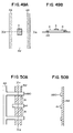
- Fig. 6A is a plan view of this DC type gas-discharge display panel
- Fig. 6B is a sectional view thereof, taken along a line X7 - X8 of Fig. 6A.
- the same reference numerals shown in Figs. 1A to 4B will be employed to denote the same elements in Figs. 6A and 6B.
- the cathode material of this panel Al, Ni, BaAl4 and the like were employed.
- the cathodes “C” were formed by directly utilizing a portion of a bus line “CB", or an adhesion of the cathode material on the bus line "CB".
- a white glass material was employed as the cell partition "BA” and a white over-glaze layer "WB” was provided.
- As a red phosphor (YGd)BO3:Eu was pasted and printed/burned.
- Zn2SiO4:Mn was pasted and printed/burned
- BaMg A114 023:Eu was pasted and printed/burned.
- the conditions of the present invention namely the conditions such as the compositions of the filling gas and total pressure thereof, were confirmed by performing various measurements, while changing the composition of the filling gases and the like in the DC type gas-discharge display panel shown in Figs. 6A and 6B, which has substantially the same construction as that of the fourth preferred embodiment.
- a He - Xe (10%) filling gas namely, a filling gas composed by a He gas with partial pressure of 90% and a Xe gas with partial pressure of 10%
- a lifetime of a display panel is considerably prolonged.
- the total pressure of 33 kPa (250 Torr) of the filling gas is increased only by 10%, the lifetime of the display panel is increased about two times and thus exceeds 10,000 hrs.
- the luminance of this panel was substantially constant at approximately 50 cd/m2.
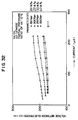
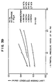
- a graphic representation as shown in Fig. 10 is obtained.
- This figure also includes measurement data for values of the current I of not only 60 ⁇ A, but also 100 ⁇ A, 150 ⁇ A, and 200 ⁇ A. It can be seen from the gradient of the curves shown in Fig. 10 that the lifetime of the panel is substantially proportional to between p5 and p6, ("p" indicates total pressure of filling gas).
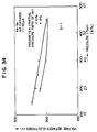
- Fig. 11 represents a lifetime-to-pressure characteristic of the display panel, as shown in Figs.
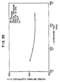
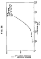
- Figs. 15 to 42 show further experimental data.
- the characteristics obtained under such conditions that the total pressure "p" of the filling gas is used as the parameter, and the total pressure "P" is selected to be 60 kPa (450 Torr), 40 kPa (300 Torr), and 27 kPa (200 Torr). It should be noted that the lifetimes of the display panel in Fig. 15 have been converted into the lifetimes under D 1/60.
- the characteristics obtained under such conditions that the total pressure "p" of the filling gas is used as the parameter, and the total pressure "P" is selected to be 20 kPa (150 Torr), 27 kPa (200 Torr), and 40 kPa (300 Torr). It should be noted that the lifetimes of the display panel in Fig. 18 have been converted into the lifetimes under D 1/60.
- Fig. 25 there are shown characteristics obtained when the partial pressure ratio of the Xe gas is used as the parameter, and this partial pressure ratio is selected to be 4%, 10%, 20% and 40%.
- Fig. 26 there are shown characteristic obtained when the partial pressure ratio of the kr gas is used as the parameter, and this partial pressure is selected to be 0%, 1%, 4% 10% and 45%.
- Fig. 29 there are shown characteristics obtained when the partial pressure ratio of the Xe gas is used as the parameter, and this partial pressure is selected to be 20%, 10% and 4%.
- Fig. 30 there are shown characteristics obtained when the partial pressure ratio of the Xe gas is used as the parameter, and this partial pressure is selected to be 40%, 20%, 10% and 4%.
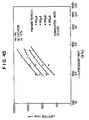
- the total pressure "p" of the filling gas is used as the parameter, and the total pressure "P" is selected to be 20, 27, 33, 40, 47 and 60 kPa (150, 200, 250, 300, 350 and 450 Torr).
- Fig. 33 there are shown characteristic obtained when the partial pressure ratio of the Xe gas is used as the parameter, and this partial pressure ratio is selected to be 40%, 20%, 10% and 4%.
- Fig. 34 there are shown characteristics obtained when the partial pressure ratio of the Xe gas is used as the parameter, and this partial pressure ratio is selected to be 10% and 4%.
- Fig. 38 there are shown characteristics obtained when the partial pressure ratio of the Xe gas is used as the parameter, and this partial pressure ratio is selected to be 20%, 10% and 4%.
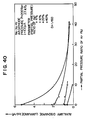
- Fig. 40 there are shown characteristics obtained when the partial pressure ratio of the Xe gas is used as the parameter, and this partial pressure ratio is selected to be 4%, 10%, 20% and 40%.
- Fig. 40 represents how to change luminance of visible Ne light in response to variations in the Kr partial pressure when only the auxiliary discharge cell of the display panel is discharged.
- Fig. 41 there are shown characteristics obtained when the partial pressure ratio of the Kr gas is used as the parameter, and this partial pressure is selected to be 0%, 4%, 10% and 40%.
- Fig. 41 indicates how to change luminance of visible Ne light in response to the Kr-partial pressure ratio when only the auxiliary discharge cell of the above-described display panel is discharged.
- the visible Ne light is contained in the above-described measurements of the luminance and the light-emission efficiency when Ne gas is contained in the filling gas.
- T max ⁇ 80xk(1-3.3x), 1 ⁇ 2.7 ⁇ 10 ⁇ 7 xp5(100/I)3 [hour] (5)
- x indicates a partial pressure ratio of Xe gas
- k denotes a partial pressure ratio of Kr gas
- symbol "p” shows total pressure (133 Pa or 1 Torr)
- symbol "I” is a current value ( ⁇ A).
- the interval is set to be 1.2 times the minimum distance "d".
- a relatively high sustain voltage e.g. 20 V
- the discharge occurring at the place of the minimum distance "d” is an abnormal glow discharge, and sputtering is rapidly increased.
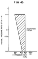
- Figs. 10, 12, 31 and 32 As shown in Fig. 57, in case of the display panel shown in Figs. 6A and 6B, abnormal glow-discharge occurs over about 2/3 area of the entire cathode area.
- an actual cathode area "S” is obtained by: Accordingly, an overall area "2lW” becomes approximately 2/3.
- the active cathode are a "S" is equal to 0.04 mm2.
- the maximum pressure values of the display panel are preferably selected to be 80 kPa (600 Torr) in case of He-Xe and He-Xe-Kr filling gases, and 67 kPa (500 Torr) in case of Ne-Xe and Ne-Xe-Kr filling gases. Also, due to the stable discharge, it is preferable to set: x ⁇ 0.5 and k ⁇ 0.5.
- the pd-product may be preferably selected to be 1 to 10 (1.3 Pa.m, 1 Torr. cm) when He-Xe and He-Xe-Kr filling gases are filled, and 0.5 to 10 (1.3 Pa.m, 1 Torr. cm) when Ne-Xe and Ne-Xe-Kr filling gases are filled. Also, taking account of the light-emission efficiency, it is preferable to set: 0.01 ⁇ x.
- a write voltage for a memory drive of a display panel must be higher than a sustain voltage by several tens of Volts, for example, 50 V, such a write voltage may cause a large current flow in this display panel, as apparent from Figs. 31 and 32, thus shortening the lifetime thereof. Therefore, a certain type of current limiting element must be connected in series with the display panel. Normally, since a resistor is employed, this resistor may be connected as shown in Figs. 4A and 4B.
- the lifetime of a display panel having a Ni cathode is shorter than that having an Al cathode.
- mercury Hg
- Other cathode materials include BaAl4, LaB6, BaB6, Ba(N3)2, an alkali metal, Y203, ZnO, RuO2, Cr, Co, graphite, Ca 0.2 La 0.8 BCrO3, Mg, BaLa2O4 , BaAl2O4, and LaCrO3, and there are substantially similar effects.
- Adhesive methods usable for the above-described cathode materials include printing, plasma melt-injection, vapour deposition and sputtering methods etc.
- the red phosphor comprises: Y203: Eu, YVO3: Eu, YP 0.65 V 0.35 04,: Eu, YBO3: Eu, or (YGa)BO3: Eu.
- green phosphor the following may be employed Zn2SiO4: Mn, BaMg2Al14O24: Eu, Mn, or BaAl12O19: Mn.
- blue phosphor the following may be used: Y2SiO4: Ce, YP 0.85 V 0.15 04,: Eu, BaMg2Al14O24,: Eu, or BaMgAl14,023: Eu.
- the adhesive methods used for the above-described phosphor materials include printing, photoetching, photo-tacking, and spray methods etc.
- the place to which the phosphor is adhered determines the display panel type; a reflection type display panel has phosphor adhered to the back plate or cell wall plate, whilst a transmission type display panel has phosphor adhered to the front plate.
- the positioning of the resistor depends upon the type of display panel. When the phosphor is attached to the front plate there are limitations as to where the resistor can be connected, thus there is greater design freedom in the reflection type display panel than in the transmission type display panel.
- a filter to achieve high contrast may be included in the panel as described more in detail in publication (3).
- the structures of the display panels may be realized as shown in publications (4) and (5). There are shown other structure examples in Figs. 46A and 46B., In Figs. 46A and 46B, the same reference numerals as used in Figs. 1A to 4B are employed as those to denote the same elements.
- This cell structure has a feature that a resistor "R" is connected to a front plate "FG", and the remaining structures are substantially identical to those of Figs. 4A and 4B.
- Figs. 47A and 47B there is shown another example in which a resistor is connected only to a write electrode. It should be noted that the same reference numerals are employed to denote the same elements as shown in Figs. 47A and 47B.
- a cathode is provided on the front plate, and a write anode bus line (WAB) extends vertically over a back plate which is connected via a resistor (R) to a write anode (WA).
- WAB write anode bus line
- WA write anode
- the display anode (DA) projects from a bus line (DAB) thereof toward a cell center unit.
- This bus line “DAB” is positioned either parallel to "C”, or parallel to the write anode bus line (WAB), and since a sustain discharge operation is carried out between the bus line (DAB) and "C". In this case, the display panel is driven only in the pulse memory mode.
- Display panels are classified based upon a combination of (1) whether the resistor is connected to the front plate, or the back plate; (2) whether the electrode to which the resistor is connected is an anode, a cathode, or a write electrode; and (3) whether or not an auxiliary discharge is present. These combinations may be conceived as the above-described two examples, or as other examples. If these display panels are combined with other display panels as shown in Figs. 48A to 51B (will be discussed later), display panels with conspicuous characteristics may be obtained.
- the display panels according to the present invention may be driven in either drive mode.
- the power consumption of a sustain pulse is small in structure in which the cathode is positioned parallel to a display anode bus line.
- Fig. 48A is a plan view for showing a portion of a DC type gas-discharge display panel according to another preferred embodiment of the present invention
- Fig. 48B is a sectional view of this display panel, taken along a line X13 to X14 shown in Fig. 48A.
- a resistive material "RM” is formed in a band shape in such a manner that under one pair of parallel anode bus lines "AB", the size of this resistive material is larger than the size of the anode bus line "AB”, and the band-shaped resistive material is positioned over a plurality of discharge cells "DCE” in common to the anode bus line "AB".
- An anode “A” is formed at substantially the center of two anode bus lines "AB”, and a resistor "R” is terminated by this anode together with the anode bus line "AB".
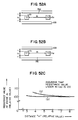
- Figs. 52A to 52C conditions on the distances between the adjoining anodes “A” positioned along a direction of the anode bus line "AB” will be described.
- Figs. 52A and 52B if the sizes of the anodes A1 and A2 are 2x2, the distance between the anodes A1 and A2, and the anode bus line "AB" is 1, and the distance between the adjoining anodes A1 and A2 is "m", resistance values of a resistor terminated by the anode A1 and the anode bus line "AB” are calculated if (a) the potential of the adjoining anode A2 is the same as that of the anode bus line "AB" (0V), and (b) the potential of the adjoining anode A2 is equal to that of the anode A1 (1V).
- the calculated resistance values are shown in Fig. 52C. As a consequence, if the distance "m", is greater than, or equal to 6, it can be seen that the influence of
- resistor "R” is not adversely influenced by fluctuations appearing in the shape or size of the resistive material "RM”. Also, this resistance value is not adversely influenced by the edges or end portions of the resistive material where the thickness of the resistive material RM fluctuates most. As a consequence, a lack of luminous uniformity, or luminous variation of each gas-discharge cell can be reduced without requiring high precision during production.
- Figs. 54A to 55B represent calculation results with respect to the adverse influences of the sizes of the anode "A" to the resistance values, variations parallel to the anode bus line "AB", and variation perpendicular thereto.
- precision along the parallel direction to the anode bus line AB should be below 2%
- precision along the direction perpendicular to the anode bus line should be below 1.3%.
- the shape of the resistor employed in the discharge display panel according to the present invention is not limited to that shown in Figs. 48A and 48B, but may be such a shape that, for instance, the anode bus line AB is located under the resistive material RM as shown in Figs. 49A and 49B.
- the resistive material RM may be formed in such a manner that this resistive material "RM" extends outside of the anode bus line "AB".
- the resistive material "RM" may extend only to the outer edge or the central portion of the anode bus line "AB" thereon.
- a resistor "R” may be formed by being terminated by a comb-shaped branch anode bus line ABO branched from the anode bus line AB and an anode formed near the center thereof.
- a resistive material "RM” is printed in a band shape along a longitudinal direction thereof by way of the thick-film printing operation, this resistive material can be easily made uniform except for the starting and ending portions of the printing operation.
- Figs. 56A and 56B the positional precision with respect to the branch anode bus line ABO of the anode A will be explained in the preferred embodiment shown in Figs. 50A and 50B.
- Fig. 56A when a distance between the anode "A" and the branch anode bus line ABO is equal to 1, and also a positional shift is "g", variations in the resistance values of the resistor R caused by the positional shift "g" are represented in Fig. 56B.
- the positional shift is 0.1 (equivalent to 10%)
- the variations in the resistance values are below 1%.
- the anode bus line "AB” may be formed under the resistive material "RM”, which is similar to the previous embodiment of Figs. 49A and 49B.
- a branch anode bus line ABC may be formed in the shape of a ladder, and an anode "A" positioned adjacent to the bus line may be separate therefrom.
- the positionsal precision between the anode "A", anode bus line “AB” and branch anode bus line ABC is up to 10% in any direction, then the variations in the resistance values are below 1%.
- the distance between the adjoining anodes "A” may be shortened, as compared with that of the preferred embodiment shown in Figs. 48A and 48B.
- the anode bus line AB may be formed under the resistive material "RM".
- resistors are formed at the anode side of the discharge cells in all of the above-described preferred embodiments, these resistors may be, of course, formed at the cathode sides.
- the cathode may be formed on the electrode for terminating the resistor. This may be applied to the anode, and material such as Ni which has high resistance against mercury which is usually employed to prolong the lifetime of a gas-discharge display panel may be stacked.
- the above-described inventive idea may be applied not only to the gas-discharge display panel as shown in Figs. 48A and 48B, but also a display panel from which luminous color of a gas discharge such as a Ne gas is directly output from the display panel, and such a display panel without an auxiliary anode.
- the present invention is not limited to the display panel having such a structure as shown in Figs. 48A and 48B, but may be applied to display panels in which, for instance, the anode is arranged in an offset relationship with the cathode, namely the anode is not positioned directly opposite to the cathode.
- the thick-film printing method is employed to manufacture the resistive materials, the bus lines for terminating the resistive materials, and the electrodes, however these parts may be manufactured by various patterning methods, for example, vapour deposition/ photolithography, and chemical etching or lift off.
- the resistive material As the resistive material, the following may be used: RuO2, a Nichrome (TM) alloy, tin oxide, Ta2N, Cr-SiO, ITO, carbon and the like. It is presently preferred to employ a thick film paste made of RuO2.
- the electrode material to terminate the resistive material there are employed Au, Pd, Ag, Al, Ni, Cu, or alloys thereof. Au was found to be best for thick-film 20 printing.
- the filling gas utilized in the present invention may be the filling gas as described above.
- Al and Ni and the like may be readily utilized.
- Ni cathode is solely employed in a display panel, the lifetime of this display panel is shorter than one with an Al cathode.
- mercury "Hg" is included in the Ni cathode, the lifetime thereof may be prolonged approximately 100 times longer than the lifetime of the display panel with only the Ni cathode, which becomes longer than that of the display panel with the Al cathode.
- cathode materials, phosphor materials and filters described regarding the first described embodiment may be utilized in the present embodiment.
Landscapes
- Gas-Filled Discharge Tubes (AREA)
- Control Of Indicators Other Than Cathode Ray Tubes (AREA)
Applications Claiming Priority (7)
| Application Number | Priority Date | Filing Date | Title |
|---|---|---|---|
| JP03202135A JP3126756B2 (ja) | 1991-07-18 | 1991-07-18 | 直流型放電パネルと表示装置 |
| JP202135/91 | 1991-07-18 | ||
| JP03301832A JP3096113B2 (ja) | 1991-11-18 | 1991-11-18 | 気体放電表示パネル |
| JP301832/91 | 1991-11-18 | ||
| JP30624791A JP3190714B2 (ja) | 1991-11-21 | 1991-11-21 | 直流型放電パネルとそれをパルスメモリ駆動する表示装置 |
| JP306247/91 | 1991-11-21 | ||
| EP92306554A EP0524005B1 (fr) | 1991-07-18 | 1992-07-16 | Panneau d'affichage à décharge de gaz en champ continu et dispositif d'affichage à décharge gazeuse l'utilisant |
Related Parent Applications (2)
| Application Number | Title | Priority Date | Filing Date |
|---|---|---|---|
| EP92306554.4 Division | 1992-07-16 | ||
| EP92306554A Division EP0524005B1 (fr) | 1991-07-18 | 1992-07-16 | Panneau d'affichage à décharge de gaz en champ continu et dispositif d'affichage à décharge gazeuse l'utilisant |
Publications (2)
| Publication Number | Publication Date |
|---|---|
| EP0649159A1 true EP0649159A1 (fr) | 1995-04-19 |
| EP0649159B1 EP0649159B1 (fr) | 1999-03-17 |
Family
ID=27328046
Family Applications (2)
| Application Number | Title | Priority Date | Filing Date |
|---|---|---|---|
| EP92306554A Expired - Lifetime EP0524005B1 (fr) | 1991-07-18 | 1992-07-16 | Panneau d'affichage à décharge de gaz en champ continu et dispositif d'affichage à décharge gazeuse l'utilisant |
| EP94120109A Expired - Lifetime EP0649159B1 (fr) | 1991-07-18 | 1992-07-16 | Panneau d'affichage à décharge dans un gaz du type courant continu |
Family Applications Before (1)
| Application Number | Title | Priority Date | Filing Date |
|---|---|---|---|
| EP92306554A Expired - Lifetime EP0524005B1 (fr) | 1991-07-18 | 1992-07-16 | Panneau d'affichage à décharge de gaz en champ continu et dispositif d'affichage à décharge gazeuse l'utilisant |
Country Status (3)
| Country | Link |
|---|---|
| US (2) | US5510678A (fr) |
| EP (2) | EP0524005B1 (fr) |
| DE (2) | DE69214040T2 (fr) |
Cited By (2)
| Publication number | Priority date | Publication date | Assignee | Title |
|---|---|---|---|---|
| EP0779643A3 (fr) * | 1995-12-15 | 1999-03-10 | Matsushita Electric Industrial Co., Ltd. | Panneau l'affichage à plasma convenant à l'affichage de haute qualité et procédé de fabrication |
| EP0936655A3 (fr) * | 1998-02-16 | 1999-12-08 | Sony Corporation | Dispositif plat d'affichage par décharge plasma |
Families Citing this family (21)
| Publication number | Priority date | Publication date | Assignee | Title |
|---|---|---|---|---|
| CA2127850C (fr) * | 1993-07-19 | 1999-03-16 | Matsushita Electric Industrial Co., Ltd. | Panneau luminescent pour l'affichage video en couleurs et son systeme d'attaque et appareil d'affichage video couleur utilisant ce panneau |
| US5877589A (en) * | 1997-03-18 | 1999-03-02 | International Business Machines Corporation | Gas discharge devices including matrix materials with ionizable gas filled sealed cavities |
| JPH1125863A (ja) * | 1997-06-30 | 1999-01-29 | Fujitsu Ltd | プラズマディスプレイパネル |
| US6255777B1 (en) | 1998-07-01 | 2001-07-03 | Plasmion Corporation | Capillary electrode discharge plasma display panel device and method of fabricating the same |
| JP2002033058A (ja) * | 2000-07-14 | 2002-01-31 | Sony Corp | 電界放出型表示装置用の前面板 |
| US6545422B1 (en) * | 2000-10-27 | 2003-04-08 | Science Applications International Corporation | Socket for use with a micro-component in a light-emitting panel |
| US6570335B1 (en) | 2000-10-27 | 2003-05-27 | Science Applications International Corporation | Method and system for energizing a micro-component in a light-emitting panel |
| US6620012B1 (en) | 2000-10-27 | 2003-09-16 | Science Applications International Corporation | Method for testing a light-emitting panel and the components therein |
| JP2002132208A (ja) * | 2000-10-27 | 2002-05-09 | Fujitsu Ltd | プラズマディスプレイパネルの駆動方法および駆動回路 |
| US7288014B1 (en) | 2000-10-27 | 2007-10-30 | Science Applications International Corporation | Design, fabrication, testing, and conditioning of micro-components for use in a light-emitting panel |
| US6764367B2 (en) * | 2000-10-27 | 2004-07-20 | Science Applications International Corporation | Liquid manufacturing processes for panel layer fabrication |
| US6796867B2 (en) * | 2000-10-27 | 2004-09-28 | Science Applications International Corporation | Use of printing and other technology for micro-component placement |
| US6762566B1 (en) | 2000-10-27 | 2004-07-13 | Science Applications International Corporation | Micro-component for use in a light-emitting panel |
| US6935913B2 (en) * | 2000-10-27 | 2005-08-30 | Science Applications International Corporation | Method for on-line testing of a light emitting panel |
| US6822626B2 (en) | 2000-10-27 | 2004-11-23 | Science Applications International Corporation | Design, fabrication, testing, and conditioning of micro-components for use in a light-emitting panel |
| US6801001B2 (en) * | 2000-10-27 | 2004-10-05 | Science Applications International Corporation | Method and apparatus for addressing micro-components in a plasma display panel |
| US6612889B1 (en) * | 2000-10-27 | 2003-09-02 | Science Applications International Corporation | Method for making a light-emitting panel |
| JP3704068B2 (ja) * | 2001-07-27 | 2005-10-05 | ザ ウエステイム コーポレイション | Elパネル |
| US20050189164A1 (en) * | 2004-02-26 | 2005-09-01 | Chang Chi L. | Speaker enclosure having outer flared tube |
| EP1569254A1 (fr) * | 2004-02-27 | 2005-08-31 | ABB Technology AG | Interrupteur de mise à la terre et/ou sectionneur |
| US9024526B1 (en) | 2012-06-11 | 2015-05-05 | Imaging Systems Technology, Inc. | Detector element with antenna |
Citations (1)
| Publication number | Priority date | Publication date | Assignee | Title |
|---|---|---|---|---|
| US4780644A (en) * | 1984-02-10 | 1988-10-25 | Nippon Hoso Kyokai | Gas discharge display panel |
Family Cites Families (5)
| Publication number | Priority date | Publication date | Assignee | Title |
|---|---|---|---|---|
| JPS52143987A (en) * | 1976-05-26 | 1977-11-30 | Dainippon Toryo Co Ltd | Gas discharge luminous eleme nt |
| JPS5830038A (ja) * | 1981-08-17 | 1983-02-22 | Sony Corp | 放電表示装置 |
| US4703229A (en) * | 1985-10-10 | 1987-10-27 | United Technologies Corporation | Optical display from XeF excimer fluorescence |
| JPS63205031A (ja) * | 1987-02-19 | 1988-08-24 | Fujitsu Ltd | ガス放電パネル |
| JP2820491B2 (ja) * | 1990-03-30 | 1998-11-05 | 松下電子工業株式会社 | 気体放電型表示装置 |
-
1992
- 1992-07-16 DE DE69214040T patent/DE69214040T2/de not_active Expired - Fee Related
- 1992-07-16 EP EP92306554A patent/EP0524005B1/fr not_active Expired - Lifetime
- 1992-07-16 DE DE69228709T patent/DE69228709T2/de not_active Expired - Fee Related
- 1992-07-16 EP EP94120109A patent/EP0649159B1/fr not_active Expired - Lifetime
-
1995
- 1995-01-27 US US08/379,969 patent/US5510678A/en not_active Expired - Lifetime
- 1995-04-06 US US08/418,155 patent/US5559403A/en not_active Expired - Fee Related
Patent Citations (1)
| Publication number | Priority date | Publication date | Assignee | Title |
|---|---|---|---|---|
| US4780644A (en) * | 1984-02-10 | 1988-10-25 | Nippon Hoso Kyokai | Gas discharge display panel |
Non-Patent Citations (2)
| Title |
|---|
| S. MIKOSHIBA ET AL.: "Mechanism of discharge build-up and high-speed addressing of a Townsend-discharge panel TV using pre-discharges.", PROCEEDINGS OF THE SID., vol. 31, no. 4, 1990, NEW YORK US, pages 349 - 354, XP000207745 * |
| TAKANO ET AL.: "Plasma display panel with a resistor in each cell.", ANNUAL CONVENTION OF THE INSTITUTE OF TELEVISION ENGINEERS OF JAPAN, no. 4-3, 1990, TOKYO, JP, pages 77 - 78 * |
Cited By (8)
| Publication number | Priority date | Publication date | Assignee | Title |
|---|---|---|---|---|
| EP0779643A3 (fr) * | 1995-12-15 | 1999-03-10 | Matsushita Electric Industrial Co., Ltd. | Panneau l'affichage à plasma convenant à l'affichage de haute qualité et procédé de fabrication |
| US5993543A (en) * | 1995-12-15 | 1999-11-30 | Masaki Aoki Et Al. | Method of producing plasma display panel with protective layer of an alkaline earth oxide |
| EP1333462A3 (fr) * | 1995-12-15 | 2007-12-05 | Matsushita Electric Industrial Co., Ltd. | Panneau d'affichage à plasma convenant à l'affichage de haute qualité et procédé de fabrication |
| USRE40647E1 (en) | 1995-12-15 | 2009-03-10 | Matsushita Electric Industrial Co., Ltd. | Method of producing plasma display panel with protective layer of an alkaline earth oxide |
| USRE40871E1 (en) | 1995-12-15 | 2009-08-18 | Panasonic Corporation | Method of producing plasma display panel with protective layer of an alkaline earth oxide |
| USRE41503E1 (en) | 1995-12-15 | 2010-08-17 | Panasonic Corporation | Method of producing plasma display panel with protective layer of an alkaline earth oxide |
| EP0936655A3 (fr) * | 1998-02-16 | 1999-12-08 | Sony Corporation | Dispositif plat d'affichage par décharge plasma |
| US6329749B1 (en) | 1998-02-16 | 2001-12-11 | Sony Corporation | Planar type plasma discharge display device |
Also Published As
| Publication number | Publication date |
|---|---|
| US5510678A (en) | 1996-04-23 |
| DE69228709D1 (de) | 1999-04-22 |
| EP0649159B1 (fr) | 1999-03-17 |
| EP0524005A2 (fr) | 1993-01-20 |
| DE69214040D1 (de) | 1996-10-31 |
| DE69214040T2 (de) | 1997-03-06 |
| DE69228709T2 (de) | 1999-07-29 |
| US5559403A (en) | 1996-09-24 |
| EP0524005B1 (fr) | 1996-09-25 |
| EP0524005A3 (fr) | 1993-02-24 |
Similar Documents
| Publication | Publication Date | Title |
|---|---|---|
| EP0649159A1 (fr) | Panneau d'affichage à décharge dans un gaz du type courant continu | |
| JP3384390B2 (ja) | 交流駆動型プラズマ表示装置 | |
| US20050174055A1 (en) | Plasma display device having barrier ribs | |
| US4780644A (en) | Gas discharge display panel | |
| JPS63205031A (ja) | ガス放電パネル | |
| US20050041001A1 (en) | Plasma display panel and manufacturing method | |
| EP0185115A1 (fr) | Dispositif d'affichage à décharge dans un gaz | |
| US20020180355A1 (en) | Plasma display device | |
| US6737805B2 (en) | Plasma display device and method of producing the same | |
| EP1093148A1 (fr) | Dispositif d'affichage à plasma | |
| JP3096113B2 (ja) | 気体放電表示パネル | |
| JP3126756B2 (ja) | 直流型放電パネルと表示装置 | |
| JP3190714B2 (ja) | 直流型放電パネルとそれをパルスメモリ駆動する表示装置 | |
| JP3481988B2 (ja) | 気体放電表示パネル | |
| JP2002042663A (ja) | 交流駆動型プラズマ表示装置及びその製造方法 | |
| US20040038615A1 (en) | Production method for plasma display panel unit-use panel and production method for plasma display unit | |
| JP2623405B2 (ja) | カラープラズマディスプレイパネル | |
| JPH0721928A (ja) | 気体放電型表示装置 | |
| JP3232899B2 (ja) | 気体放電型表示装置およびその製造方法 | |
| JP2001076630A (ja) | 交流駆動型プラズマ表示装置 | |
| JPH09120779A (ja) | ガス放電型表示パネル | |
| JP4742872B2 (ja) | プラズマディスプレイパネル | |
| JP2981444B2 (ja) | ガス放電表示パネル | |
| JP2000353473A (ja) | プラズマディスプレイ用部材およびそれを用いたプラズマディスプレイ | |
| Fujii et al. | High-performance plasma display panel with cathodes in the cell walls |
Legal Events
| Date | Code | Title | Description |
|---|---|---|---|
| PUAI | Public reference made under article 153(3) epc to a published international application that has entered the european phase |
Free format text: ORIGINAL CODE: 0009012 |
|
| AC | Divisional application: reference to earlier application |
Ref document number: 524005 Country of ref document: EP |
|
| AK | Designated contracting states |
Kind code of ref document: A1 Designated state(s): DE FR GB |
|
| 17P | Request for examination filed |
Effective date: 19950309 |
|
| 17Q | First examination report despatched |
Effective date: 19961120 |
|
| GRAG | Despatch of communication of intention to grant |
Free format text: ORIGINAL CODE: EPIDOS AGRA |
|
| GRAG | Despatch of communication of intention to grant |
Free format text: ORIGINAL CODE: EPIDOS AGRA |
|
| GRAG | Despatch of communication of intention to grant |
Free format text: ORIGINAL CODE: EPIDOS AGRA |
|
| GRAH | Despatch of communication of intention to grant a patent |
Free format text: ORIGINAL CODE: EPIDOS IGRA |
|
| GRAH | Despatch of communication of intention to grant a patent |
Free format text: ORIGINAL CODE: EPIDOS IGRA |
|
| GRAA | (expected) grant |
Free format text: ORIGINAL CODE: 0009210 |
|
| AC | Divisional application: reference to earlier application |
Ref document number: 524005 Country of ref document: EP |
|
| AK | Designated contracting states |
Kind code of ref document: B1 Designated state(s): DE FR GB |
|
| ET | Fr: translation filed | ||
| REF | Corresponds to: |
Ref document number: 69228709 Country of ref document: DE Date of ref document: 19990422 |
|
| PLBE | No opposition filed within time limit |
Free format text: ORIGINAL CODE: 0009261 |
|
| STAA | Information on the status of an ep patent application or granted ep patent |
Free format text: STATUS: NO OPPOSITION FILED WITHIN TIME LIMIT |
|
| 26N | No opposition filed | ||
| REG | Reference to a national code |
Ref country code: GB Ref legal event code: IF02 |
|
| PGFP | Annual fee paid to national office [announced via postgrant information from national office to epo] |
Ref country code: FR Payment date: 20030528 Year of fee payment: 12 |
|
| PGFP | Annual fee paid to national office [announced via postgrant information from national office to epo] |
Ref country code: GB Payment date: 20030716 Year of fee payment: 12 |
|
| PGFP | Annual fee paid to national office [announced via postgrant information from national office to epo] |
Ref country code: DE Payment date: 20030929 Year of fee payment: 12 |
|
| PG25 | Lapsed in a contracting state [announced via postgrant information from national office to epo] |
Ref country code: GB Free format text: LAPSE BECAUSE OF NON-PAYMENT OF DUE FEES Effective date: 20040716 |
|
| PG25 | Lapsed in a contracting state [announced via postgrant information from national office to epo] |
Ref country code: DE Free format text: LAPSE BECAUSE OF NON-PAYMENT OF DUE FEES Effective date: 20050201 |
|
| GBPC | Gb: european patent ceased through non-payment of renewal fee |
Effective date: 20040716 |
|
| PG25 | Lapsed in a contracting state [announced via postgrant information from national office to epo] |
Ref country code: FR Free format text: LAPSE BECAUSE OF NON-PAYMENT OF DUE FEES Effective date: 20050331 |
|
| REG | Reference to a national code |
Ref country code: FR Ref legal event code: ST |