EP0668681A2 - Selbstleitweglenkendes Vermittlungssystem - Google Patents
Selbstleitweglenkendes Vermittlungssystem Download PDFInfo
- Publication number
- EP0668681A2 EP0668681A2 EP95103947A EP95103947A EP0668681A2 EP 0668681 A2 EP0668681 A2 EP 0668681A2 EP 95103947 A EP95103947 A EP 95103947A EP 95103947 A EP95103947 A EP 95103947A EP 0668681 A2 EP0668681 A2 EP 0668681A2
- Authority
- EP
- European Patent Office
- Prior art keywords
- information
- self
- routing
- control
- input
- Prior art date
- Legal status (The legal status is an assumption and is not a legal conclusion. Google has not performed a legal analysis and makes no representation as to the accuracy of the status listed.)
- Withdrawn
Links
Images


Classifications
-
- H—ELECTRICITY
- H04—ELECTRIC COMMUNICATION TECHNIQUE
- H04L—TRANSMISSION OF DIGITAL INFORMATION, e.g. TELEGRAPHIC COMMUNICATION
- H04L49/00—Packet switching elements
- H04L49/25—Routing or path finding in a switch fabric
- H04L49/253—Routing or path finding in a switch fabric using establishment or release of connections between ports
- H04L49/254—Centralised controller, i.e. arbitration or scheduling
-
- H—ELECTRICITY
- H04—ELECTRIC COMMUNICATION TECHNIQUE
- H04L—TRANSMISSION OF DIGITAL INFORMATION, e.g. TELEGRAPHIC COMMUNICATION
- H04L49/00—Packet switching elements
- H04L49/15—Interconnection of switching modules
- H04L49/1507—Distribute and route fabrics, e.g. sorting-routing or Batcher-Banyan
-
- H—ELECTRICITY
- H04—ELECTRIC COMMUNICATION TECHNIQUE
- H04L—TRANSMISSION OF DIGITAL INFORMATION, e.g. TELEGRAPHIC COMMUNICATION
- H04L49/00—Packet switching elements
- H04L49/20—Support for services
- H04L49/205—Quality of Service based
-
- H—ELECTRICITY
- H04—ELECTRIC COMMUNICATION TECHNIQUE
- H04L—TRANSMISSION OF DIGITAL INFORMATION, e.g. TELEGRAPHIC COMMUNICATION
- H04L49/00—Packet switching elements
- H04L49/30—Peripheral units, e.g. input or output ports
- H04L49/3009—Header conversion, routing tables or routing tags
-
- H—ELECTRICITY
- H04—ELECTRIC COMMUNICATION TECHNIQUE
- H04L—TRANSMISSION OF DIGITAL INFORMATION, e.g. TELEGRAPHIC COMMUNICATION
- H04L49/00—Packet switching elements
- H04L49/30—Peripheral units, e.g. input or output ports
- H04L49/3018—Input queuing
-
- H—ELECTRICITY
- H04—ELECTRIC COMMUNICATION TECHNIQUE
- H04L—TRANSMISSION OF DIGITAL INFORMATION, e.g. TELEGRAPHIC COMMUNICATION
- H04L49/00—Packet switching elements
- H04L49/45—Arrangements for providing or supporting expansion
-
- H—ELECTRICITY
- H04—ELECTRIC COMMUNICATION TECHNIQUE
- H04L—TRANSMISSION OF DIGITAL INFORMATION, e.g. TELEGRAPHIC COMMUNICATION
- H04L49/00—Packet switching elements
- H04L49/55—Prevention, detection or correction of errors
- H04L49/552—Prevention, detection or correction of errors by ensuring the integrity of packets received through redundant connections
-
- H—ELECTRICITY
- H04—ELECTRIC COMMUNICATION TECHNIQUE
- H04L—TRANSMISSION OF DIGITAL INFORMATION, e.g. TELEGRAPHIC COMMUNICATION
- H04L49/00—Packet switching elements
- H04L49/55—Prevention, detection or correction of errors
- H04L49/555—Error detection
Definitions
- the present invention relates to an N x N (where N is a natural number, same below) or N x M self-routing switching system having N number of incoming lines and N or M number of outgoing lines which is optimal for use for high-speed packet switching or asynchronous transfer mode switching.
- a Banyan type self-routing speech path is constructed based on the principle of dichotomization, so expansion of scale is achieved by combining two N x N switches and N number of 2 x 2 switches to make a 2N x 2N switch.
- the increases are in units of multiples of 2.
- a modular construction is difficult and it is necessary to relay all the wirings on the outgoing line side. Therefore, there are practical inconveniences as a speech path built into a self-routing switching system.
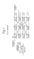
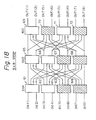
- FIG. 3 is a view showing a first embodiment of a speech path in a self-routing switching system according to the present invention.
- the self-routing speech path 30 of the first embodiment is comprised of one or a plurality of basic switching units.
- a speech path 30 comprised of a single basic switching unit is shown.
- This basic switching unit is comprised of an input stage self-routing switch module (SRM) 31, a middle stage self-routing switch module (SRM) 32, and an output stage self-routing switching module (SRM) 33.
- SRM input stage self-routing switch module
- SRM middle stage self-routing switch module
- SRM output stage self-routing switching module
- multiple link connection is used for the SRM ij 's.
- the input stage SRM switches SRM 11 to SRM 1N/n have n number of input ends and m number of output ends and are N/n in number
- the middle stage SRM 12 modules SRM 21 to SRM 2m have N/n number of input ends and N/n number of output ends and are m in number
- the output stage SRM modules SRM 31 to SRM 3n/N have m number of input ends and n number of output ends and are n/N in number.
- L ij are the primary links
- M ij the secondary links.
- the input ends of the input stage modules (31) SRM 11 to SRM 1N/n are connected to the incoming lines, while the output ends are connected to the input ends of the middle stage modules 32.
- the m number of output ends of the SRM 11 are connected to one of the input ends of the m number of middle stage SRM modules SRM 21 to SRM 2m .
- the SRM 1N/n module etc. are similarly connected.
- the N/n number of output ends of the middle stage modules are connected to one of the m number of input ends of the outgoing line side N/n number of modules SRM 31 to SRM 3N/n .
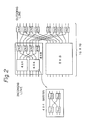
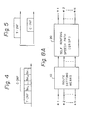
- FIG 4 is a view showing a first example of a format of information appearing on an incoming line of a self-routing switch path.
- Figure 5 is a view showing a second example of a format of information appearing on an incoming line of a self-routing switch path.
- the packet or cell entering the incoming line is given control information (C.INF) RH 1 , RH 2 , & RH n comprised of routing headers, as shown in Figs. 4 and 5.
- This may be in series with the transmission information (T.INF) such as in Fig. 4 or in parallel such as in Fig. 5.
- the latter case, of course, requires an exclusive control information line.
- the control information RH, , RH 2 Hence shows the number of the ith order link, i.e., the number of the output end of the ith stage switch module.
- the switch modules view the number and guide the transmission information to the said link, i.e., the designated output end.
- the required number (m number) of middle stage switch modules SRM 21 to SRM 2m are provided. If less than the possible number (N/n number) of input and output stage switch modules are provided, then in expansion it is merely necessary to add input and output stage switch modules and perform wiring for the input and output stage switch modules. At this time, there is no need to make any changes on the already installed switch modules or their wiring.
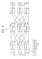
- the primary links L 11 , L 12 , and L 1 connect the three output ends of the input stage switch module SRM 11 to the first top input ends of the middle stage switch modules SRM 21 to SRM 23 .
- the primary links L 21 to L 23 and L 31 to L 33 follow this.
- the secondary links M 11 to M 13 connect the three output ends of the middle stage switch module SRM 21 to the first input ends of the three switch modules SRM 31 to SRM 33 of the output stage.
- the secondary links M 21 to M 23 and M 31 to M 33 follow the same.
- a selector control circuit SC j for example, continually scans for a request signal R ij from an FIFO memory FM ij and, when a request signal R ij is detected, operates so that the contents of that FIFO memory FM are output through a selector SEL i .
- a request signal R ij is input to a selector control circuit SC j as an interruption input and, when an interruption occurs, the selector control circuit SC j outputs the content of the said FIFO memory FM through the selector SEL.
- FIFO memories FM ij are given a capacity corresponding to a plurality of packets or cells, a buffer function is obtained and sufficient response is possible even when the transmission data increases temporarily.
- Fig. 3 to Fig. 7 it is possible to change the number of incoming and outgoing lines without changing the existing wiring.
- the amount of change is not limited to multiples of 2.
- the change can be made in units of the number of input and output ends of the switch modules.
- the self-routing speech path 10 may have a plurality of paths linking between the incoming and outgoing lines, so there is little delay even with congestion.
- CP 1 controls SWITCH 1 to connect link 0 to link, and adds the virtual channel number VCN, after exchanging VCNo to VCN1.
- the operations of CP 2 - CP n - 1 are the same as the above operation of CP1.
- CP n When CP n detects the virtual channel number VCN n , it ercognizes the receipt of a packet for terminal Y, so that CP n controls SWITCH n to transfer the received packet to terminal Y.
- the route setting means 10 monitors the above-mentioned identification information from the information of the incoming lines and forms control information C.INF in accordance with this identification information.
- the self-routing speech path (SRSP) 20 of the present invention has built in it a buffer memory means which holds temporarily at least the transmission information (if necessary, both the transmission information and control information) which can make time adjustments on information transfer in the self-routing speech path (SRSP) 20.
- SRSP self-routing speech path
- the second, third, fourth, and fifth embodiments of the self-routing speech path (SRSP) 20 are respectively shown in the later-mentioned Figs. 29 and 30, Figs. 31 to 34, Figs. 35 to 37, and Figs. 38 to 39.
- the switching information of the switch modules to which the packet is input that is, the control information C.INF, i.e., RH 1 , RH 2 , and RH 3 , and the virtual channel number for the next link are stored in the address corresponding to the identification information (VCN) which indicates the receiving party.
- the control information C.INF i.e., RH 1 , RH 2 , and RH 3
- VCN identification information
- This packet is actually transmitted in the packet transfer phase.
- This packet is comprised of the transmission information and the header portion consisting of the identification information (VCNo) added to the header of the transmission information.
- the synchronizing circuit 17 synchronizes with the incoming packet for the use of a synchronizing pattern in a header portion, and controls the timing of each part.
- the packet which is transferred to the speech path is stored in the buffer 13 of the addition circuit 11-1, and the identification information portion I.INF is input to the decoder 19 via the register 18 under the control of the synchronizing circuit 17.
- the decoder 19 receives the identification information (virtual channel number VCN o ) of the input packet, the table 16 is accessed using this identification information VCN o as the address.
- the right block numbers of the RH's show output lines of SRM 11 , SRM12 SRM 13
- the middle block numbers of the RH's show output lines of SRM 21 , SRM 22 , SRM 23
- the left block numbers of the RH's show output lines of SRM 31 , SRM 32 , SRM 33 .
- k x m and m x k means that there are two types of SRM's with different numbers of input ends and output ends.
- the self-routing switch modules used are not limited to 2 x 4 or 4 x 2 ones. It is sufficient that there be two types of modules with differing numbers of input ends and output ends.
- the number of incoming lines and outgoing lines of the expanded self-routing speech path is not limited to 8 x 8, of course.
- the number of connection stages of the self-routing speech path is determined by the relationship between the number of incoming lines and outgoing lines and is not limited to the illustrated three stages.
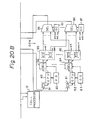
- FIG 20 is a circuit diagram of a self-routing switching system showing details, in particular, of the portion of the optional service module of Fig. 19. Portions other than the optional service modules are the same in construction as in Fig. 9.
- a predetermined single switch module SRM 2m located at the middle stage of the self-routing switch modules SRM of the self-routing switching system shown in Fig. 9 is changed to an optional service module OSM.
- one each of the output ends of the input stage switch modules SRM, to SRM1 N/n are connected to the input ends of the optional service module OSM and the output ends of the optional service module OSM are connected to one each of the input ends of the modules SRM 31 to SRM 3N/n .
- the call processor 12 sets a routing header RH to the optional service module OSM in the addition circuit (11) connected to the said terminal equipment based on the virtual channel number (VCN) in the identification information received, adds the routing header information and optional service demand to the transmission information packet, and sends the result to switch module SRM i 1 for example, at the input stage.
- the optional service module OSM is selected from the routing header as the module of the middle stage.
- Figure 24 is a view showing an example of the protocol construction of error control.
- hardware interface is performed for transmitting and receiving information.
- packet sequential control etc. Is performed and, at C.INF layer 3, an optional service demand etc. is made.
- packet identification and other packet control is performed, while at the option portion of the T.INF layer 2, the sequence of the option control is set.
- the layer3 of T.INF has set therein procedures for special control of calls.
- the transfer requests ( * 1, * 2, ... * n-1 * n) from the FIFO memories 85 are shifted one by one and input to the individual selectors (SEL) 90.
- SEL individual selectors
- the adder 94 adds the commanded value of the counter 11 and the transfer request number ( * 1, * 2, ... * n-1, * n) shown by the output of the encoder 93 and issues the corresponding FIFO memory number and sends it to the selector (SEL) 86 of Fig. 20.
- the fixed priority level decision circuit 92 sends transfer request signals to the encoder 93 by a predetermined priority order (for example, the order from the top of the illustration).
- the optional service module for executing optional services is replaced by a predetermined module of the middle stage in the self-routing switching system of the modular construction of Fig. 9 and made exclusive for optional services, so it is possible to flexibly add optional services without changing the construction of the overall switching system and to simplify the hardware construction and protocol.
- Figure 26 is a concept view of a self-routing switching system able to perform priority processing.
- the input information of the incoming line requiring the priority-processing is selected and sent on a priority basis.
- FIG. 27 is a circuit diagram showing a specific example of a self-routing switch module for performing the priority processing.
- This module SRM is shown as having a similar construction to the module OSM shown in Fig. 20, but basically it is completely equivalent to the module SRM of Fig. 7 and the modules SRM's of Fig. 16 and 17.
- the self-routing switch module SRM is provided with a signal distributor SD which transmits and receives signals with respect to the microprocessor (MPU) 15 (Fig. 12) of the call processor via a control bus 96.
- the selector control circuits (SC) 97 have a somewhat different construction from the circuit SC shown in Fig. 7. Note that as a specific example of the circuit SC of Fig. 7, it is possible to use the circuit SC shown in Fig. 25.
- controller 105 sends to the selector (SEL) 106 on a priority basis the information of the predetermined FIFO memory 85 upon command from the microprocessor (MPU).
- the selector 106 selects one of the priority information by command of the microprocessor (MPU) or output of the counter 91.
- Other constructions are the same as in Fig. 25.
- the addition circuit adds the routing header to the input information and sends the same to, for example, the module SRM, of the input stage.
- the module SRM views the routing header and transfers the information to the module SRM 21 of the middle stage.
- the information is sent through the fixed priority level decision circuit 92, encoder 93, and adder (ADD) 94 to the selector (SEL) 86 shown in Fig. 27.
- the selector (SEL) 86 selects the memory of the topmost section of the FIFO memory 85 and sends it to the modules SRM 31 to SRM 3N/n at their input ends.
- the selector control circuit (SC) 97 of Fig. 27 receives as input the transfer requests ( * 1 to ** n) (same as R in Fig. 7) from the FIFO memories 85. Along with this, the storage states of the FIFO memories 85 are input as overload signals ##1 to ##n. These overload signals can be set based on the criteria of information of a certain value or more stored in the FIFO memories.
- the selectors 90 of Fig. 28 are controlled so that the transfer request * 1 is selected. Further, when there are a plurality of FIFO memories in an overload state, selection is made by the fixed priority level decision circuit 92.
- the packet information stored in an overload state FIFO memory is sent out from the modules SRM on a priority basis without route modification.
- Figure 29 is a principle block diagram of a second embodiment of the self-routing speech path.
- the self-routing switch module SRM shown in Fig. 7 provision was made of FIFO memories to avoid packet collisions due to concentration of transfer information, e.g., packets, at the same output end.
- N 2 FIFO memories are required. Therefore, an increase in the number of incoming lines and outgoing lines results in an expotential increase in the number of requisite FIFO memories.
- the content to be stored in the FIFO memories is the packet as a whole.
- the storage capacity of the FIFO memories is set to enable storage of a plurality of packets.
- FIFO memories with large storage capacities are required.
- the storage capacity of the FIFO memories is set large, since the probability of occurrence of packet collisions is not high, usually use is not made of all the storage regions of the FIFO memories and the efficiency of use of the memories is not high.
- a self-routing speech path which can deal with an increase in the number of incoming lines and outgoing lines without a major increase in the memory means and which can use the memory means with a high efficiency.
- Fig. 29 there are provided a plurality of incoming lines #1 to #N and a plurality of outgoing lines #1 to #M, with inputs to each incoming line. Transmission information with routing headers is autonomously switched to outgoing lines designated based on the routing headers.
- a converting means 111 converts the transmission information input in parallel from the plurality of incoming lines to a time-series format.
- a transmission information storing means 112 stores sequentially the transmission information T.INF sequentially sent from the converting means 111.
- a write address storing means 113 stores the addresses for accessing the transmission information storing means 112 and sequentially gives the same to the transmission information storing means 112 as write addresses.
- a plurality of read address storing means 114(1) to 114-(M) are provided corresponding to the plurality of outgoing lines.
- An address distributing means 115 based on the routing header RH of the transmission information which is sent from the write address storing means 113 and stored in the address of the means 112, stores addresses in the read address storing means 114 corresponding to the outgoing line designated by the routing header.
- the address selecting means 116 sequentially reads out the stored read addresses from the read address storing means 114(1) to 114(M) and, using the same, reads the transmission information from the transmission information storing means 112.
- the distributing means 117 distributes the read transmission information to the outgoing line corresponding to the destination of the transmission information. Further, the read addresses read from the read address storing means 114(1) to 114(M) are again stored in the write address storing means 113 and used for address designation of the transmission information storing means 112.
- FIG. 30 is a circuit diagram showing a specific example for realizing the second embodiment of Fig. 29.
- the time-division multiplexer (MUX) 121 holds N number of incoming lines #1 to #N and performs time-division multiplexing on the packets P(1) to P(N) input in parallel to the incoming lines #1 to #N to place them in a time-series format and sends them to the input highway HW1.
- the input highway HW1 is connected to the data input terminal Dl of a random access memory (RAM) 122.
- the packets on the input highway HW1 are successively stored in the RAM 122.
- the address designation for the RAM 122 is performed using the addresses stored in the idle address memory 124.
- the idle address memory 124 is comprised of an FIFO memory and has a capacity able to store a number of addresses corresponding to the number of addresses of the RAM 122.
- the address output from the idle address memory 124 is led to the write address input terminal WA of the RAM 122 and the input terminal of the address distributor (DS) 126.
- the address distributor 126 is switched and controlled by the routing header copier (RHC) 128 and the input address is stored in one of the outgoing line FIFO memories 125(1) to 125(M).
- M number of FIFO memories 125(1) to 125(M) are provided corresponding to the M number of outgoing lines #1 to #M accommodated in a time-division demultiplexer 123. These have a capacity able to store a plurality of addresses for avoiding collision of packets in the outgoing lines #1 to #M.
- the routing header copier 128 is connected to the highway HW1.
- the routing header RH of the packet on the input highway HW1 is read and given to the address distributor 126.
- the operation of the second embodiment will be described below. Assume that packets P(1) to P(N) are input to the incoming lines #1 to #N of the time-division demultiplexer.
- the packets P(1) to P-(N) are comprised of the transmission information T.INF and routing headers RH.
- the time-division multiplexer 121 executes time-division multiplexing on the packets P(1) to P(N) to rearrange them into a time-series data format and sends the same to the input highway HW1. Therefore, the transmission speed on the input highway HW1 is N times the transmission speed on the incoming lines #1 to #N.
- These packets P(1) to P(N) are stored successively in the RAM 122.
- the address designation on the RAM 122 at this time is performed by using the addresses successively read from the idle address memory 124 as write addresses.
- the addresses read from the idle address memory 124 are sent to the RAM 122 and, simultaneously, stored in one of the FIFO memories 125(1) to 125(M) through the address distributor 126.
- the packet P(1) is written at the address position of the RAM 122 designated by the address from the idle address memory 124.
- the address is allocated to and stored in the FIFO memory 125(2) corresponding to the destination of the packet P(1), i.e., the outgoing line #2, under the control of the routing header copier 128 and address distributor 126.
- the plurality of addresses are stored in the FIFO memory 125(2).
- the packets P(1) to P(N) are successively stored in the RAM 122.
- the address information of the RAM 122 in which the packets P(1) to P(N) are stored is stored in the outgoing line address FIFO memory 125 corresponding to the destination outgoing lines of the packets P(1) to P(N).
- the reading of the packets P(1) to P(N) stored in the RAM 122 is performed by having the address selector 127 successively select the FIFO memories 125(1) to 15(M), in that order, by timing of clocks from the clock generator 129, reading the addresses stored therein, and applying the same to the RAM 122 as read addresses.
- packets are successively sent to the time-division demultiplexer 123 from the RAM 122 via the output highway HW2.
- the addresses selected by the address selector 127 are simultaneously sent to the idle address memory 124 and reused as write addresses of the packets to the RAM 122.
- the time-division demultiplexer 123 allocates the input packets successively to the outgoing lines #1 to #M such that, for example, the packet read by the address from the FIFO memory 125(1) is sent to the outgoing line #1, the packet read by the address from the FIFO memory 125(2) is sent to the outgoing line #2, ... and the packet read by the address from the FIFO memory 125(k) is sent to the outgoing line #k.
- the packets P(1) to P-(N) input to the incoming lines #1 to #N are sent to the destination outgoing line designated by the routing headers RH.
- the memory means necessary for constructing the self-routing speech path may be a RAM or other memory for storing the packets, an idle address memory for storing the idle addresses of the RAM, and outgoing line address memories 125 of a number corresponding to the outgoing lines for storing the read addresses of the RAM.
- the idle address memory 14 and outgoing line address memories 125 by small capacity memories able to just store the addresses of the RAM 122. Still further, it is possible to raise the efficiency of use of the RAM 122 storing the packet information. Note that when the RAM capacity is very large, the idle address memory 124 is not necessary.
- 131 is a self-routing speech path, which self-routing speech path 131 has N number of incoming lines 132 and N number of outgoing lines 133.
- Reference numerals 134 show memory means, which memory means 134 are provided corresponding to the N number of incoming lines 132.
- the output lines of the memory means 134 are connected to the N number of outgoing lines 133 through the latch groups 135.
- the memory means 134 are memories which operate at a speed of N + 1 times the transmission speed of the incoming lines.
- the control means 136 detect the routing headers from the input information of the incoming lines 132, cause the memory means 134 to operate at a speed of N + 1 times the incoming line transmission speed, and, simultaneously, designate the addresses and performing writing and reading with respect to the memory means 134. At this time, the memory means 134 are written at one of the phases in the N + 1 speed and read out to the N number of outgoing lines 133 during the remaining N phases.
- the transmission information read to the outgoing lines 133 is suitably latched by the related latch groups 135 and output.
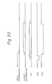
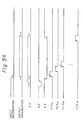
- Figure 32 is a timing chart showing signal waveforms appearing at principal portions of Fig. 31. It shows, from the top, the input information, output information, address control signal AD, write control signal WE, and read control signal RE.
- Figure 33 is a circuit diagram showing a specific example for realizing the third embodiment of Fig. 31.
- 131 is a self-routing speech path, which self-routing speech path 131 has N number of incoming lines and N number of outgoing lines.
- Reference numerals 134 show buffer memories used as the memory means. These buffer memories 134 are provided corresponding to the N number of incoming lines 132. The output lines of the buffer memories 134 are connected to the N number of outgoing lines 133 through the latch groups 135. Further, the buffer memories 134 are designed to operate at a speed of N + 1 times the transmission speed of the incoming lines.
- N number of latch groups 135 are provided corresponding to the buffer memories 134. Further, the latch groups 135 have N number of latches (flip-flops) 139.
- the routing header detection circuits 137 detect the routing headers from the input information of the incoming lines 132 and input the routing headers to the buffer memory controllers 136. At this time, the transmission information is sent from the routing header detection circuit 137 to the corresponding buffer memory 134.
- the buffer memory controllers 136 output latch control signals CLK ij -(where i and j are both 1 to N) to the latches 139.
- the output information read to the outgoing line 133 is suitably latched by the corresponding one of the latch groups 135 and output to the require outgoing line 133.
- Figure 34 is a timing chart showing signal waveforms appearing at principal portions of Fig. 33. It shows, from the top, the input information, output information, address control signal AD, write control signal WE, i.e., write enable, read control signal RE, i.e., read enable, and latch control signals CLK, i CLKi2 , CLK13 , ... and CLK 1 n .
- the write control signal WE and read control signal SE indicate “enable” at the L level and the latch control signal (clock) CLK ij indicates “data latch” at the H level.
- the latch control signals differ by one clock in each phase.
- the buffer memories 134 are operated at a speed of N + 1 times the incoming line (outgoing line) transmission speed, writing is performed at one of the phases in the N + 1 speed, and reading is performed to the N number of outgoing lines during the remaining N phases, the number of memories (memories corresponding to the FIFO memories FM of Fig. 7) can be reduced to 1/N and, thereby, the size of the circuit can be reduced.
- the intent of the fourth embodiment is, like the afore-mentioned second embodiment, to reduce the number of memory means.
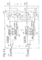
- Figure 35 is a principle block diagram of the fourth embodiment of the self-routing speech path.
- 141 is a self-routing speech path, which self-routing speech path 141 has N number of incoming lines 132 and N number of outgoing lines 133.
- Reference numerals 144 show memory means, which memory means 144 are provided corresponding to the N number of outgoing lines 133.
- the memory means 144 are memories which operate at a speed of N + 1 times the transmission speed of the incoming lines.
- Reference numerals 146 show control means, which control means 146 control the speed conversion means 145, control the selectors (SEL) 147, and control writing and reading with respect to the memory means 144. That is, due to the control means 146, the memory means 144 are operated at a speed of N + 1 times the incoming line transmission speed, the information of the N number of incoming lines is written under time division during N phases in the speed of N + 1, and the information is read to the outgoing lines 133 at the remaining one phase.
- the selectors 147 suitably allocate the input information from the speed conversion means 145 to the memory means 144 corresponding to the outgoing lines.
- Reference numerals 148 are OR gates, which OR gates 148 enable the write control signals from the control means 146 to be supplied to the memory means 144.
- the input information of the incoming lines 132 is converted by the speed conversion means 145 to a speed N + 1 times the incoming line transmission speed.
- the control means 146 detect the routing headers from the input information and send the control signals VCK ; (iis 1 to n) to the speed conversion means 145, whereby, input information from the speed conversion means 145 is sent to the memory means 144.
- Figure 37 is a circuit-diagram showing a specific example for realizing the fourth embodiment of Fig. 35.
- 141 is self-routing speech path, which self-routing speech path 141 has N number of incoming lines 132 and N number of outgoing lines 133.
- Reference numerals 144 show buffer memories used as the memory means. These buffer memories 144 are provided corresponding to the N number of outgoing lines 133. The buffer memories 144 are constructed as FIFO memories. Further, the buffer memories 144 are designed to operate at a speed of N + 1 times the transmission speed of the incoming lines.
- Reference numerals 147 are selectors, which selectors 147 receive the selector control signal SCK ; from the controllers 146 and suitably allocate the transmission information T.INF from the speed converters 145 to the desired buffer memories 144 corresponding to the outgoing lines.
- Reference numerals 148 are OR gates, which OR gates 148 enable supply of the write control signals WCK ij from the control means 146 to the buffer memories 144.
- the speed converters 145 convert the transmission information to a speed N + 1 times the incoming line transmission speed.
- the controllers 146 receive the routing headers RH, view the destinations of the input information, and control the selectors 147 by the selector control signals SCK ; (i being 1 to n) for switching to the buffer memories 144 corresponding to the destination outgoing lines and further control the clock VCK i for reading the transmission information from the speed converters 145, the clocks WCK ij (i and j being respectively 1 to n) for sharing and writing the N number of buffer memories 144, and the clocks RCK i for reading from the buffer memories 144.
- the output information read to the outgoing lines 133 is latched by the latches 150, which are actuated in synchronization with the clocks RCK; for return to the original incoming line transmission speed, and output to the required outgoing lines.
- the latches 150 which are actuated in synchronization with the clocks RCK; for return to the original incoming line transmission speed, and output to the required outgoing lines.
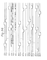
- FIG. 36 at the rising edge of the write clock WCK ij , writing is performed on the buffer memories 144.
- reading is performed from the buffer memories 144 and also latching is performed by the latches 150.
- the write clocks WCK 11 to WCK 1n (..., WCK n1 to WCK nn ) differ in phase by one clock each.
- the buffer memories 144 are operated at a speed of N + 1 times the incoming line (outgoing line) transmission speed, information of the N number of incoming lines is written under the time division method during the N phases in the N + 1 speed, and reading is performed to the outgoing lines at the remaining one phase, the number of memories corresponding to the FIFO memories FM of Fig. 7 can be reduced to 1/N and, thereby, the size of the circuit can be reduced.
- the intent of the fifth embodiment is, like the afore-mentioned second embodiment, to reduce the number of memory means.
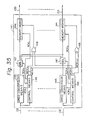
- FIG 38 is a principle block diagram of the fifth embodiment of a self-routing speech path.
- the self-routing speech path of the fifth embodiment has a plurality of incoming lines and a plurality of outgoing lines and sends input information, including routing headers, input from the incoming lines to the outgoing lines specified by the routing headers.
- a plurality of storing circuits 151 to 153 are provided corresponding to the incoming lines and temporarily store the input information input therefrom.
- a switch circuit 154 connects spatially the output terminals of the plurality of storing circuits 151 to 153 and the plurality of outgoing lines, in accordance with both the output signals and the control signals from the circuits 151 to 153.
- a memory circuit 155 has led to it in parallel, as address input, routing headers of the input information, e.g., packets, stored in the plurality of storing circuits 151 to 153 and holds the transmission permission signals to be sent to the plurality of storing circuits 151 to 153 as data corresponding to those addresses and control signals to be sent to the switching circuit 154.
- the input information e.g., packets
- the input information input to the incoming lines is held temporarily in the storing circuits 151 to 153.
- the routing headers RH of the input information are taken in parallel and given to the memory circuit 155 as its address input.
- the memory circuit 155 holds both the transmission permission signals and control signals corresponding to the addresses and sends the same to the storing circuits 151 to 153 and the switch circuit 154.
- the switch circuit 154 is switched by the control signal and the selected input information is sent out to the outgoing lines corresponding to the routing headers. This operation is successively repeated so that the input information for which collision has occurred is successively sent out to the same outgoing lines under the time division method.
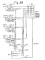
- Figure 39 is a circuit diagram showing a specific example for realizing the fifth embodiment of Fig. 38.
- the self-routing speech path is illustrated as having 4 x 4 incoming and outgoing lines.
- 132(1) to 132(4) indicate the incoming lines, 162(1) to 162(4) transmission information buffers comprised of FIFO memories, 163(1) to 163(4) routing header buffers comprised of FIFO memories, 164(1) to 164(4) routing header registers, 165 an arbitration memory, 166 a matrix switch, 133(1) to 133(4) outgoing lines, 168 a transmission permission line, and 169 a control line.
- the input information input to the incoming lines 132(1) to 132(4) is stored in the transmission information buffers 162(1) to 162(4).
- the routing headers are stored in the routing header buffers 163(1) to 163(4).
- the routing headers are read successively from the routing header buffers 163(1) to 163(4) and stored temporarily in the routing header registers 164(1) to 164(4).
- the outputs of the routing header registers 164(1) to 164(4) are given to the arbitration memory 165 as address signals.
- the routing headers determine unilaterally to which outgoing line the input information of which incoming line is output.
- the words corresponding to the addresses are read from the arbitration memory 165 and sent to the transmission information buffers 162(1) to 162-(4) as transmission permission signals and to the matrix switch 166 as crosspoint signals.
- the transmission permission signals determine if the buffers 162(1) to 162(4) may sent out the stored information or if they should hold off on transmission for a while.
- the matrix switch 166 performs switching so that the path between the buffers 162(1) to 162(4) and the outgoing lines 133(1) to 133(4) is built so the input information of the incoming lines 132(1) to 132(4) is sent to the outgoing lines corresponding to the routing headers.
- the arbitration memory 165 makes only one of the transmission permission signals sent to the buffers 162-(1) to 162(4) "1", gives transmission permission to the said transmission information buffer, and outputs the stored transmission information to the desired outgoing line through the matrix switch 166. On the other hand, it makes the other transmission information buffers hold off on the transmission of the input information. This operation is successively repeated so that the input information for which collision has occurred is successively sent out on to the same outgoing line.
- the fifth embodiment may be modified in various ways.
- the arbitration memory may be made of a read only memory (ROM) and its content fixed.
- ROM read only memory
- a RAM may be used and rewriting performed under external control.
- the embodiment shown was for a self-routing speech path with 4 x 4 inputs and outputs, but the invention is not limited to this and can be applied to self-routing speech paths of P x Q (where P and Q are integers of 2 or higher) as well.
- N number of buffers for holding the input information temporarily are sufficient.
- the number of buffers can be greatly reduced, thus enabling more compact and inexpensive apparatuses.
- the content of the arbitration processing during collisions can be easily changed by just changing the content of the arbitration memory.
- the present invention may be used for switching network of voice, facsimile data, computer data, and other switching data, in particular for high speed packet switching networks and high speed asynchronous transfer mode switching networks.
Landscapes
- Engineering & Computer Science (AREA)
- Computer Networks & Wireless Communication (AREA)
- Signal Processing (AREA)
- Data Exchanges In Wide-Area Networks (AREA)
- Telephonic Communication Services (AREA)
Applications Claiming Priority (19)
| Application Number | Priority Date | Filing Date | Title |
|---|---|---|---|
| JP26164/87 | 1987-02-06 | ||
| JP2616487 | 1987-02-06 | ||
| JP6355487 | 1987-03-18 | ||
| JP63554/87 | 1987-03-18 | ||
| JP6355587 | 1987-03-18 | ||
| JP63555/87 | 1987-03-18 | ||
| JP12029687 | 1987-05-19 | ||
| JP120296/87 | 1987-05-19 | ||
| JP121054/87 | 1987-05-20 | ||
| JP12105487 | 1987-05-20 | ||
| JP176466/87 | 1987-07-15 | ||
| JP17646687 | 1987-07-15 | ||
| JP17595087 | 1987-07-16 | ||
| JP175950/87 | 1987-07-16 | ||
| JP231816/87 | 1987-09-16 | ||
| JP23181787 | 1987-09-16 | ||
| JP231817/87 | 1987-09-16 | ||
| JP23181687 | 1987-09-16 | ||
| EP88901461A EP0300061B1 (de) | 1987-02-06 | 1988-02-05 | Selbstsuchendes vermittlungssystem |
Related Parent Applications (2)
| Application Number | Title | Priority Date | Filing Date |
|---|---|---|---|
| EP88901461.9 Division | 1988-02-05 | ||
| EP88901461A Division EP0300061B1 (de) | 1987-02-06 | 1988-02-05 | Selbstsuchendes vermittlungssystem |
Publications (1)
| Publication Number | Publication Date |
|---|---|
| EP0668681A2 true EP0668681A2 (de) | 1995-08-23 |
Family
ID=27576792
Family Applications (2)
| Application Number | Title | Priority Date | Filing Date |
|---|---|---|---|
| EP88901461A Expired - Lifetime EP0300061B1 (de) | 1987-02-06 | 1988-02-05 | Selbstsuchendes vermittlungssystem |
| EP95103947A Withdrawn EP0668681A2 (de) | 1987-02-06 | 1988-02-05 | Selbstleitweglenkendes Vermittlungssystem |
Family Applications Before (1)
| Application Number | Title | Priority Date | Filing Date |
|---|---|---|---|
| EP88901461A Expired - Lifetime EP0300061B1 (de) | 1987-02-06 | 1988-02-05 | Selbstsuchendes vermittlungssystem |
Country Status (5)
| Country | Link |
|---|---|
| US (1) | US4993018A (de) |
| EP (2) | EP0300061B1 (de) |
| CA (1) | CA1297567C (de) |
| DE (1) | DE3856469T2 (de) |
| WO (1) | WO1988005982A2 (de) |
Cited By (3)
| Publication number | Priority date | Publication date | Assignee | Title |
|---|---|---|---|---|
| GB2316572A (en) * | 1996-08-14 | 1998-02-25 | Fujitsu Ltd | Multicast switch |
| US6016307A (en) * | 1996-10-31 | 2000-01-18 | Connect One, Inc. | Multi-protocol telecommunications routing optimization |
| US6473404B1 (en) | 1998-11-24 | 2002-10-29 | Connect One, Inc. | Multi-protocol telecommunications routing optimization |
Families Citing this family (46)
| Publication number | Priority date | Publication date | Assignee | Title |
|---|---|---|---|---|
| US5072440A (en) * | 1989-03-01 | 1991-12-10 | Fujitsu Limited | Self-routing switching system having dual self-routing switch module network structure |
| EP0384936B1 (de) * | 1989-03-03 | 1994-06-15 | Siemens Aktiengesellschaft | Verfahren und Schaltungsanordnung zum Weiterleiten von auf Zubringerleitungen übertragenen Nachrichtenpaketen über eine Paketvermittlungseinrichtung |
| DE8905982U1 (de) * | 1989-05-12 | 1989-07-13 | Siemens AG, 1000 Berlin und 8000 München | Mehrstufige Koppeleinrichtung |
| US5210744A (en) * | 1989-06-28 | 1993-05-11 | Mitsubishi Denki Kabushiki Kaisha | Cell exchange apparatus |
| JP2837182B2 (ja) * | 1989-08-04 | 1998-12-14 | 富士通株式会社 | セルデータの伝送方法、送信要求処理方法及びスイッチ |
| JPH03104451A (ja) * | 1989-09-19 | 1991-05-01 | Fujitsu Ltd | 多段リンク交換システムのルート切替え方式 |
| US5313590A (en) * | 1990-01-05 | 1994-05-17 | Maspar Computer Corporation | System having fixedly priorized and grouped by positions I/O lines for interconnecting router elements in plurality of stages within parrallel computer |
| JPH03220836A (ja) * | 1990-01-25 | 1991-09-30 | Nec Corp | 非同期伝送モード交換装置 |
| US5285444A (en) * | 1990-02-09 | 1994-02-08 | Hitachi, Ltd. | Multi-stage link switch |
| JPH03268532A (ja) * | 1990-03-19 | 1991-11-29 | Fujitsu Ltd | Atmセルのブロードキャスト方式 |
| KR920009679B1 (ko) * | 1990-06-27 | 1992-10-22 | 재단법인 한국전자통신연구소 | 스위칭 메모리를 갖는 고속 atm 셀 동기 교환장치 |
| EP0471256A3 (en) * | 1990-08-10 | 1993-08-04 | Hitachi, Ltd. | Atm switch and atm multiplexer |
| SE467079B (sv) * | 1990-09-19 | 1992-05-18 | Ellemtel Utvecklings Ab | Saett och anordning foer adressering i ett paketnaet |
| JPH04156140A (ja) * | 1990-10-19 | 1992-05-28 | Fujitsu Ltd | Atmスイッチの障害検出方式 |
| JPH04291872A (ja) * | 1991-03-20 | 1992-10-15 | Fujitsu Ltd | 同報通信方式及びスイッチングシステム |
| JP3023721B2 (ja) * | 1991-09-09 | 2000-03-21 | 富士通株式会社 | Srm間ハイウエイ接続方法および装置 |
| JPH0583291A (ja) * | 1991-09-19 | 1993-04-02 | Fujitsu Ltd | Atm試験方式 |
| JP3110104B2 (ja) * | 1991-10-07 | 2000-11-20 | 富士通株式会社 | 交換機 |
| JP2671699B2 (ja) * | 1991-11-15 | 1997-10-29 | 三菱電機株式会社 | セル交換装置 |
| US5398235A (en) * | 1991-11-15 | 1995-03-14 | Mitsubishi Denki Kabushiki Kaisha | Cell exchanging apparatus |
| US5452295A (en) * | 1992-03-18 | 1995-09-19 | Fujitsu Limited | Call disconnection method and exchange executing the same in ATM network |
| US5309433A (en) * | 1992-06-18 | 1994-05-03 | International Business Machines Corp. | Methods and apparatus for routing packets in packet transmission networks |
| EP0597205B1 (de) * | 1992-09-07 | 2003-04-09 | Hitachi, Ltd. | Multiprozessorsystem und Kommunikationsverfahren zwischen Prozessoren |
| EP0608653A1 (de) * | 1993-01-26 | 1994-08-03 | International Business Machines Corporation | Verfahren und Vorrichtung zur Informationweglenkung zwischen Knoten in einem Kommunikationsnetz |
| DE69433229T2 (de) * | 1993-02-15 | 2004-08-12 | Mitsubishi Denki K.K. | ATM-Schalter |
| US5371735A (en) * | 1993-03-04 | 1994-12-06 | International Business Machines Corporation | Communication network with non-unique device identifiers and method of establishing connection paths in such a network |
| JP3357423B2 (ja) * | 1993-06-15 | 2002-12-16 | 富士通株式会社 | 交換システム付設装置のための制御システム |
| US5696764A (en) * | 1993-07-21 | 1997-12-09 | Fujitsu Limited | ATM exchange for monitoring congestion and allocating and transmitting bandwidth-guaranteed and non-bandwidth-guaranteed connection calls |
| JP3178949B2 (ja) * | 1993-09-30 | 2001-06-25 | 富士通株式会社 | Atmスイッチ方式 |
| JP3291122B2 (ja) * | 1994-06-02 | 2002-06-10 | 富士通株式会社 | 自己ルーチング交換機、atm交換機及び交換システム |
| CH690603A5 (it) * | 1995-04-28 | 2000-10-31 | Giancarlo Borsetto | Dispositivo di connessione per lo smistamento di segnali elettrici. |
| US5787086A (en) * | 1995-07-19 | 1998-07-28 | Fujitsu Network Communications, Inc. | Method and apparatus for emulating a circuit connection in a cell based communications network |
| US5721820A (en) * | 1995-09-11 | 1998-02-24 | International Business Machines Corporation | System for adaptively routing data in switching network wherein source node generates routing message identifying one or more routes form switch selects |
| AU6970896A (en) * | 1995-09-14 | 1997-04-01 | Ascom Nexion Inc. | Transmitter controlled flow control for buffer allocation in wide area atm networks |
| DE19539406C2 (de) * | 1995-10-11 | 1998-07-23 | Mannesmann Ag | Verfahren zum Weiterleiten von sprachungebundenen Informationen |
| AU1697697A (en) * | 1996-01-16 | 1997-08-11 | Fujitsu Limited | A reliable and flexible multicast mechanism for atm networks |
| US5748905A (en) * | 1996-08-30 | 1998-05-05 | Fujitsu Network Communications, Inc. | Frame classification using classification keys |
| EP1021757A1 (de) * | 1997-07-25 | 2000-07-26 | Starvox, Inc. | Verfahren und vorrichtung für integriertes sprach-gateway |
| DE19961269A1 (de) * | 1999-12-18 | 2001-06-21 | Alcatel Sa | Netzwerkknoten zum Vermitteln von digitalen Informationen unterschiedlicher Protokolltypen |
| US7065076B1 (en) * | 2000-08-25 | 2006-06-20 | Promise Technology, Inc. | Modular scalable switching networks |
| JP4588259B2 (ja) * | 2000-09-11 | 2010-11-24 | 富士通株式会社 | 通信システム |
| ES2211753T3 (es) * | 2000-09-29 | 2004-07-16 | Alcatel | Priorizador de tareas en una matriz de interconexion. |
| US7797444B2 (en) * | 2003-02-03 | 2010-09-14 | Nippon Telegraph And Telephone Corporation | Data transfer apparatus and data transfer system |
| FI120430B (fi) * | 2004-11-16 | 2009-10-15 | Abb Oy | Räätälöitävä taajuusmuuttaja |
| CN101404616A (zh) * | 2008-11-04 | 2009-04-08 | 北京大学深圳研究生院 | 一种负载均衡分组交换结构及其构造方法 |
| DE102013019643A1 (de) * | 2013-11-22 | 2015-05-28 | Siemens Aktiengesellschaft | Zweistufiger Kreuzschienenverteiler und Verfahren zum Betrieb |
Family Cites Families (11)
| Publication number | Priority date | Publication date | Assignee | Title |
|---|---|---|---|---|
| SE381548B (sv) * | 1974-12-20 | 1975-12-08 | Ellemtel Utvecklings Ab | Anordning for omstyrning av veljarnet |
| US4173713A (en) * | 1977-02-07 | 1979-11-06 | International Telephone & Telegraph Corporation | Continuously expandable switching network |
| FR2469849A1 (fr) * | 1979-09-08 | 1981-05-22 | Plessey Overseas | Module de commutation temporelle et reseau numerique a plusieurs etages |
| FR2538976A1 (fr) * | 1982-12-29 | 1984-07-06 | Servel Michel | Systeme de commutation de paquets synchrones de longueur fixe |
| US4550397A (en) * | 1983-12-16 | 1985-10-29 | At&T Bell Laboratories | Alternate paths in a self-routing packet switching network |
| US4630259A (en) * | 1984-11-14 | 1986-12-16 | At&T Bell Laboratories | Lockup detection and recovery in a packet switching network |
| US4651318A (en) * | 1984-11-30 | 1987-03-17 | At&T Bell Laboratories | Self-routing packets with stage address identifying fields |
| US4641302A (en) * | 1985-06-24 | 1987-02-03 | Racal Data Communications Inc. | High speed packet switching arrangement |
| US4731878A (en) * | 1985-11-29 | 1988-03-15 | American Telephone And Telegraph Company, At&T Bell Laboratories | Self-routing switch node combining electronic and photonic switching |
| BE904100A (fr) * | 1986-01-24 | 1986-07-24 | Itt Ind Belgium | Systeme de commutation. |
| GB2188813B (en) * | 1986-04-01 | 1990-03-14 | Stc Plc | Switching network |
-
1988
- 1988-02-01 CA CA000557830A patent/CA1297567C/en not_active Expired - Lifetime
- 1988-02-05 WO PCT/JP1988/000113 patent/WO1988005982A2/en not_active Ceased
- 1988-02-05 EP EP88901461A patent/EP0300061B1/de not_active Expired - Lifetime
- 1988-02-05 US US07/280,723 patent/US4993018A/en not_active Expired - Lifetime
- 1988-02-05 EP EP95103947A patent/EP0668681A2/de not_active Withdrawn
- 1988-02-05 DE DE3856469T patent/DE3856469T2/de not_active Expired - Fee Related
Cited By (9)
| Publication number | Priority date | Publication date | Assignee | Title |
|---|---|---|---|---|
| GB2316572A (en) * | 1996-08-14 | 1998-02-25 | Fujitsu Ltd | Multicast switch |
| GB2316572B (en) * | 1996-08-14 | 2000-12-20 | Fujitsu Ltd | Multicasting in switching apparatus |
| US6349097B1 (en) | 1996-08-14 | 2002-02-19 | Fujitsu Limited | Multicasting in switching apparatus |
| US6016307A (en) * | 1996-10-31 | 2000-01-18 | Connect One, Inc. | Multi-protocol telecommunications routing optimization |
| US6456594B1 (en) | 1996-10-31 | 2002-09-24 | Connect One, Llp | Multi-protocol communications routing optimization |
| US7307956B2 (en) | 1996-10-31 | 2007-12-11 | Connectel, Llc | Multi-protocol telecommunications routing optimization |
| US9036499B2 (en) | 1996-10-31 | 2015-05-19 | Patentmarks Communications, Llc | Multi-protocol telecommunications routing optimization |
| US9806988B2 (en) | 1996-10-31 | 2017-10-31 | Patentmarks Communications, Llc | Multi-protocol telecommunications routing optimization |
| US6473404B1 (en) | 1998-11-24 | 2002-10-29 | Connect One, Inc. | Multi-protocol telecommunications routing optimization |
Also Published As
| Publication number | Publication date |
|---|---|
| EP0300061B1 (de) | 2001-05-23 |
| DE3856469T2 (de) | 2002-05-23 |
| WO1988005982A3 (en) | 1988-12-29 |
| US4993018A (en) | 1991-02-12 |
| CA1297567C (en) | 1992-03-17 |
| EP0300061A1 (de) | 1989-01-25 |
| WO1988005982A2 (en) | 1988-08-11 |
| DE3856469D1 (de) | 2001-06-28 |
Similar Documents
| Publication | Publication Date | Title |
|---|---|---|
| US4993018A (en) | Self-routing switching system with multiple link connections between incoming and outgoing lines | |
| AU693084B2 (en) | Controlled access ATM switch | |
| JP2595025B2 (ja) | 空間分割形スイッチを用いた高速パケット交換装置 | |
| Garcia-Haro et al. | ATM shared-memory switching architectures | |
| CA1264081A (en) | Distributed voice-data switching on multi-stage interconnection networks | |
| US4893304A (en) | Broadband packet switch with combined queuing | |
| EP0195589B1 (de) | Vermittlungssystem für Datenübertragung | |
| US7116633B2 (en) | Packet switching system and method | |
| US4752777A (en) | Delta network of a cross-point switch | |
| EP0471344A1 (de) | Verfahren und Schaltung zur Verkehrsformung | |
| CA2224606C (en) | A distributed buffering system for atm switches | |
| JPH10313323A (ja) | パケットスイッチング装置及びこれを用いたパケットスイッチングシステム | |
| JPH08293877A (ja) | 通信システム | |
| JPH0418518B2 (de) | ||
| JPH08307432A (ja) | 通信方法 | |
| US5128927A (en) | Switching network and switching network control for a transmission system | |
| Obara et al. | High speed transport processor for broad-band burst transport system | |
| JP2755402B2 (ja) | 自己ルーチング交換システムおよび非同期転送モード交換システム | |
| JPH022766A (ja) | 交換ノード | |
| JP2962667B2 (ja) | 非同期転送モード交換システム | |
| JPH08214008A (ja) | 自己ルーチングスイッチ | |
| KR0178797B1 (ko) | 통신 교환 모듈 | |
| JPH08214007A (ja) | 自己ルーチングスイッチモジュール | |
| KR100220640B1 (ko) | Atm-pbx의 입력 버퍼형 atm스위치 | |
| JP3124642B2 (ja) | Atm交換機の系切替え方法 |
Legal Events
| Date | Code | Title | Description |
|---|---|---|---|
| PUAI | Public reference made under article 153(3) epc to a published international application that has entered the european phase |
Free format text: ORIGINAL CODE: 0009012 |
|
| AC | Divisional application: reference to earlier application |
Ref document number: 300061 Country of ref document: EP |
|
| AK | Designated contracting states |
Kind code of ref document: A2 Designated state(s): DE FR GB IT SE |
|
| RIN1 | Information on inventor provided before grant (corrected) |
Inventor name: IWABUCHI, EISUKE Inventor name: TACHIBANA, TETSUO, DAIICHI-SHINJO-RYO Inventor name: ISONO, OSAMU Inventor name: FUKUI, TOSHIMASA, KIZUKISUMIYOSHI-DANCHI 3-32 Inventor name: NISHINO, TETSUO, YAJIMA-MANSHION 303 Inventor name: ABE, SHUNJI, NYUPASUKAMIOOKA 606 Inventor name: MURAKAMI, KOSO Inventor name: HAJIKANO, KAZUO |
|
| STAA | Information on the status of an ep patent application or granted ep patent |
Free format text: STATUS: THE APPLICATION HAS BEEN WITHDRAWN |
|
| 18W | Application withdrawn |
Effective date: 20040304 |