EP0674786B1 - Dispositif a unites fonctionnelles enfichables - Google Patents
Dispositif a unites fonctionnelles enfichables Download PDFInfo
- Publication number
- EP0674786B1 EP0674786B1 EP94902605A EP94902605A EP0674786B1 EP 0674786 B1 EP0674786 B1 EP 0674786B1 EP 94902605 A EP94902605 A EP 94902605A EP 94902605 A EP94902605 A EP 94902605A EP 0674786 B1 EP0674786 B1 EP 0674786B1
- Authority
- EP
- European Patent Office
- Prior art keywords
- plug
- peripheral functional
- level
- station
- way
- Prior art date
- Legal status (The legal status is an assumption and is not a legal conclusion. Google has not performed a legal analysis and makes no representation as to the accuracy of the status listed.)
- Expired - Lifetime
Links
Images

Classifications
-
- G—PHYSICS
- G05—CONTROLLING; REGULATING
- G05B—CONTROL OR REGULATING SYSTEMS IN GENERAL; FUNCTIONAL ELEMENTS OF SUCH SYSTEMS; MONITORING OR TESTING ARRANGEMENTS FOR SUCH SYSTEMS OR ELEMENTS
- G05B19/00—Program-control systems
- G05B19/02—Program-control systems electric
- G05B19/04—Program control other than numerical control, i.e. in sequence controllers or logic controllers
- G05B19/042—Program control other than numerical control, i.e. in sequence controllers or logic controllers using digital processors
- G05B19/0423—Input/output
-
- G—PHYSICS
- G06—COMPUTING OR CALCULATING; COUNTING
- G06F—ELECTRIC DIGITAL DATA PROCESSING
- G06F12/00—Accessing, addressing or allocating within memory systems or architectures
- G06F12/02—Addressing or allocation; Relocation
- G06F12/06—Addressing a physical block of locations, e.g. base addressing, module addressing, memory dedication
- G06F12/0646—Configuration or reconfiguration
- G06F12/0684—Configuration or reconfiguration with feedback, e.g. presence or absence of unit detected by addressing, overflow detection
-
- G—PHYSICS
- G06—COMPUTING OR CALCULATING; COUNTING
- G06F—ELECTRIC DIGITAL DATA PROCESSING
- G06F13/00—Interconnection of, or transfer of information or other signals between, memories, input/output devices or central processing units
- G06F13/14—Handling requests for interconnection or transfer
- G06F13/20—Handling requests for interconnection or transfer for access to input/output bus
- G06F13/24—Handling requests for interconnection or transfer for access to input/output bus using interrupt
-
- G—PHYSICS
- G06—COMPUTING OR CALCULATING; COUNTING
- G06F—ELECTRIC DIGITAL DATA PROCESSING
- G06F13/00—Interconnection of, or transfer of information or other signals between, memories, input/output devices or central processing units
- G06F13/38—Information transfer, e.g. on bus
- G06F13/40—Bus structure
- G06F13/4063—Device-to-bus coupling
- G06F13/4068—Electrical coupling
- G06F13/4072—Drivers or receivers
-
- G—PHYSICS
- G05—CONTROLLING; REGULATING
- G05B—CONTROL OR REGULATING SYSTEMS IN GENERAL; FUNCTIONAL ELEMENTS OF SUCH SYSTEMS; MONITORING OR TESTING ARRANGEMENTS FOR SUCH SYSTEMS OR ELEMENTS
- G05B2219/00—Program-control systems
- G05B2219/20—Pc systems
- G05B2219/21—Pc I-O input output
- G05B2219/21049—Poll and detect connected I-O modules, address terminator, address line high
-
- G—PHYSICS
- G05—CONTROLLING; REGULATING
- G05B—CONTROL OR REGULATING SYSTEMS IN GENERAL; FUNCTIONAL ELEMENTS OF SUCH SYSTEMS; MONITORING OR TESTING ARRANGEMENTS FOR SUCH SYSTEMS OR ELEMENTS
- G05B2219/00—Program-control systems
- G05B2219/20—Pc systems
- G05B2219/21—Pc I-O input output
- G05B2219/21071—Configuration, each module has a settable address, code wheel, encoder
-
- G—PHYSICS
- G05—CONTROLLING; REGULATING
- G05B—CONTROL OR REGULATING SYSTEMS IN GENERAL; FUNCTIONAL ELEMENTS OF SUCH SYSTEMS; MONITORING OR TESTING ARRANGEMENTS FOR SUCH SYSTEMS OR ELEMENTS
- G05B2219/00—Program-control systems
- G05B2219/20—Pc systems
- G05B2219/21—Pc I-O input output
- G05B2219/21089—Detect configuration of I-O regulary
Definitions
- the invention relates to an arrangement according to the preamble of claim 1.
- German patent application P 42 39 030.3 proposes an arrangement in which a CPU unit suitable for carrying out read and / or write accesses can be plugged into each slot.
- the arrangement is provided with a plurality of slots which are connected to one another via a system bus having data and control lines, and with address lines routed to connecting means of the slots, one of which is connected to a selection connection of a slot.
- the CPU unit has means for connecting to the address lines, and each of the remaining functional units is provided with means for connecting to the selection port of the slot. In this arrangement, the CPU unit cannot recognize whether the slots are equipped with functional units.
- a processor is known from the publication "EDN Electrical Design News", Vol. 26, No. 3, February 1981 (Mackintosh), which is provided for recognizing the position of a unit in a rack. For this purpose, the processor supplies the slot provided for this unit with an address assigned to this unit. The data bus is used to report whether this unit is plugged into this slot. An address is provided for each unit and multiple accesses are required to determine the position in the rack for each unit.
- a data processing system with a processor unit is known from EP-A-0 324 144, which events can be supplied by peripheral units in the form of interrupt signals are. Measures to identify slots are not planned.
- the present invention has for its object to provide an arrangement of the type mentioned, in which the CPU unit recognizes slots equipped with functional units.
- the arrangement according to the invention is used in particular in a programmable logic controller, preferably in a programmable logic controller with a central device and at least one expansion device, which are connected to one another via a connecting cable which has the system and address bus, the address lines and further address lines for addressing the expansion device.
- slots SP1... SP4 are designated, which are connected to one another via a system bus SYB having several data and control lines.
- peripheral units PE1, PE2, PE4 and one for executing read and / or write access Suitable CPU unit CP for which the slots SP1 ... SP4 and the units corresponding connection means, for. B. in the form of spring and knife contacts.
- the functional units PE1, PE2 PE4 and the CPU unit CP are arbitrary in the Slots SP1 ... SP4 pluggable.
- the first address line AL1 is connected via a line SL1 to the selection connection AN1 of the slot SP1.
- the address lines AL2, AL3, AL4 are connected via lines SL2, SL3, SL4 to the selection connections AN2, AN3, AN4 of the slots SP2, SP3, SP4.
- These address lines AL1 ... AL4 are each connected via a resistor R to a log. "1" corresponding potential.
- the CPU unit CP To address the peripheral units PE1, PE2, PE4, the CPU unit CP generates an address signal in the form of a log. "0", which is supplied via the address lines AL1, AL2, AL4 and via the lines SL1, SL2, SL4 to the selection connections AN1, AN2, AN4.
- the CPU unit CP is addressed via the address line AL3, the line SL3 and the selection connection AN3 by further units which are not shown here and are suitable for carrying out read and / or write accesses.
- the CPU unit CP applies a slot identification signal in the form of a signal log to the slot connecting line JD cyclically or during predefinable times of a time switching of the CPU unit CP. "1", which is fed to the slots SP1, SP4 and thus not shown level switching means of the peripheral units PE2, PE4. In this example, only those are peripheral units PE2 and PE4, whereby their level switching means switch the level of the address lines AL2, AL4 assigned to the units PE2, PE4.
- the CPU unit CP recognizes on the basis of the level of the address lines AL1, AL2, AL4 that only the peripheral units PE2, PE4 are plugged into the slots SP2, SP4.
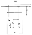
- FIG. 2 The function and mode of operation of level switching means is illustrated in FIG. 2.
- the same parts in Figures 1 and 2 are provided with the same reference numerals.
- the peripheral unit PE2 has level switching means in the form of a transistor TR connected to resistors R1, R2, the control connection of which is connected to the slot connecting line JD.
- the collector of the transistor is led to the connection point of an input amplifier EV with the address line AL2, and the emitter is at a log level. "0" corresponding ground potential connected.
- Other parts of the peripheral unit PE2 are of no importance for the invention and therefore do not need to be explained.
- the CPU unit CP ( Figure 1) leads the transistor TR via the slot connecting line JD the slot identification signal in the form of a log. "1”, the transistor TR becomes conductive and connects the address line AL2 to the ground potential. As a result, the level on the address line AL2 of log. "1" on log. "0” switched. In the event that the peripheral unit PE2 is not inserted in the slot SP2, the level on the address line AL2 is not changed, since the address line AL2 is connected to a log via the resistor R. "1" corresponding potential is laid.
- the CPU unit CP asks cyclically or for predefinable times of a time monitoring circuit the CPU unit CP from the levels of the address lines AL1, AL2, AL4.
- level switching means first switch the level of the respective address line AL1, AL2, AL4 and then the level of an acknowledgment display line.
- the switched level on the receipt display line indicates to the CPU unit CP that the read access has been completed.
- the CPU unit CP immediately recognizes the address lines AL1, AL2, AL4 to which the levels have been switched, which indicate which locations are equipped with functional units.
- the receipt display line is connected to connection means of the slots SP1, SP4, and the units PE1, PE2, PE4, CP have connection means for contacting the receipt display line.
- the level switching means also have a further transistor, the collector of which is connected to the acknowledgment line and the emitter of which is connected to ground potential. This transistor is also triggered with a time delay using the slot identification signal. Furthermore, it is possible to provide one of the control or data lines of the system bus SYB instead of the slot connecting line JD for transmitting the slot identification signal, so that the slot connecting line is no longer required.
Landscapes
- Engineering & Computer Science (AREA)
- Theoretical Computer Science (AREA)
- General Physics & Mathematics (AREA)
- Physics & Mathematics (AREA)
- General Engineering & Computer Science (AREA)
- Computer Hardware Design (AREA)
- Automation & Control Theory (AREA)
- Bus Control (AREA)
- Coupling Device And Connection With Printed Circuit (AREA)
- Details Of Connecting Devices For Male And Female Coupling (AREA)
- Connector Housings Or Holding Contact Members (AREA)
- Stored Programmes (AREA)
- Programmable Controllers (AREA)
- Small-Scale Networks (AREA)
Claims (5)
- Dispositif comportant plusieurs emplacements (SP1, ...) d'enfichage, qui sont reliés entre eux par l'intermédiaire d'un bus (SYB) de système comportant des conducteurs de données et des conducteurs de commande et par l'intermédiaire d'un bus (AB) d'adresse et dans lesquels sont enfichées les unités CPU (CP) appropriées pour l'exécution d'accès en lecture et/ou en écriture et plusieurs unités fonctionnelles périphériques (PE1, PE2, PE4), des emplacements (SP1, ...) d'enfichage équipés d'unités pouvant être indiqués à l'unité CPU (CP),
caractérisé en ce que- le dispositif comporte des conducteurs d'adresse (AL1, AL2, AL3, AL4), chacun de ces conducteurs d'adresse (AL1, AL2, AL4) étant reliés à une borne de sélection (AN1, AN2, AN3, AN4) d'un emplacement d'enfichage par l'intermédiaire d'un conducteur supplémentaire (SL1, SL2, SL3, SL4),- les unités fonctionnelles périphériques (PE1, PE2, PE4) et l'unité CPU (CP) sont munies de moyens de raccordement à l'une des bornes de sélection (AN1, AN2, AN3, AN4) et de moyens de raccordement à un conducteur (JD) de liaison d'emplacement d'enfichage, par l'intermédiaire duquel un niveau de signal d'identification d'emplacement d'enfichage peut être envoyé aux unités fonctionnelles périphériques (PE1, PE2, PE4) par l'unité CPU (CP),- les unités fonctionnelles périphériques (PE1, PE2, PE4) sont munies chacune d'un moyen de commutation de niveau, chaque moyen de commutation de niveau commutant, dans le cas où l'unité fonctionnelle périphérique (PE1, PE2, PE4) reçoit un niveau de signal d'identification d'emplacement d'enfichage, le niveau du signal d'adresse associé à cette unité fonctionnelle périphérique (PE1, PE2, PE4) par l'intermédiaire de la borne de sélection, ce qui indique à l'unité (CP) l'occupation de cet emplacement d'enfichage. - Dispositif suivant la revendication 1, caractérisé en ce que- l'unité CPU (CP) envoie aux moyens de commutation de niveau le niveau de signal d'identification d'emplacement d'enfichage cycliquement ou pendant des temps pouvant être prescrits.
- Commande par programme enregistré comportant un dispositif suivant la revendication 1 ou 2.
- Commande par programme enregistré comportant un appareil central comportant un dispositif suivant la revendication 1 ou 2 et au moins un appareil d'extension, qui est relié par l'intermédiaire d'un câble de liaison lequel comporte le bus de système et un bus d'adresse (SYB, AB), les conducteurs d'adresse (AL1, ...) et d'autres conducteurs d'adresse pour l'adressage de l'appareil d'extension.
- Unité fonctionnelle périphérique (PE1, PE2, PE4), qui peut être enfichée dans l'un des emplacements (SP1, ...) d'enfichage d'un dispositif suivant la revendication 1 ou 2,
caractérisée en ce que- l'unité fonctionnelle périphérique (PE1, PE2, PE4) est munie de moyens de raccordement à la borne (AN1, AN2, AN3, AN4) de sélection de l'emplacement d'enfichage respectif et de moyens de raccordement au conducteur (JD) de liaison d'emplacement d'enfichage, par l'intermédiaire duquel le niveau de signal d'identification d'emplacement d'enfichage peut être envoyé à l'unité fonctionnelle périphérique (PE1, PE2, PE4) par l'unité CPU (CP),- l'unité fonctionnelle périphérique (PE1, PE2, PE4) est munie d'un moyen de commutation de niveau, qui commute, dans le cas où l'unité fonctionnelle périphérique (PE1, PE2, PE4) reçoit le niveau de signal d'identification d'emplacement d'enfichage, le niveau du signal d'adresse associé à cette unité fonctionnelle périphérique (PE1, PE2, PE4) par l'intermédiaire de la borne de sélection (AN1, AN2, AN3, AN4), ce qui indique à l'unité CPU l'occupation de cet emplacement d'enfichage.
Applications Claiming Priority (5)
| Application Number | Priority Date | Filing Date | Title |
|---|---|---|---|
| DE4243347A DE4243347A1 (de) | 1992-12-21 | 1992-12-21 | Anordnung mit steckbaren Funktionseinheiten |
| DE19924243348 DE4243348A1 (de) | 1992-12-21 | 1992-12-21 | Anordnung mit steckbaren Funktionseinheiten |
| DE4243348 | 1992-12-21 | ||
| DE4243347 | 1992-12-21 | ||
| PCT/DE1993/001213 WO1994015299A1 (fr) | 1992-12-21 | 1993-12-17 | Dispositif a unites fonctionnelles enfichables |
Publications (2)
| Publication Number | Publication Date |
|---|---|
| EP0674786A1 EP0674786A1 (fr) | 1995-10-04 |
| EP0674786B1 true EP0674786B1 (fr) | 1997-03-19 |
Family
ID=25921592
Family Applications (1)
| Application Number | Title | Priority Date | Filing Date |
|---|---|---|---|
| EP94902605A Expired - Lifetime EP0674786B1 (fr) | 1992-12-21 | 1993-12-17 | Dispositif a unites fonctionnelles enfichables |
Country Status (6)
| Country | Link |
|---|---|
| EP (1) | EP0674786B1 (fr) |
| AT (1) | ATE150561T1 (fr) |
| DE (1) | DE59305909D1 (fr) |
| DK (1) | DK0674786T3 (fr) |
| ES (1) | ES2099579T3 (fr) |
| WO (1) | WO1994015299A1 (fr) |
Cited By (1)
| Publication number | Priority date | Publication date | Assignee | Title |
|---|---|---|---|---|
| EP0952523A1 (fr) * | 1998-04-22 | 1999-10-27 | PHOENIX CONTACT GmbH & Co. | Unité fonctionnelle pour une commande programmable par mémoire avec une fonction de redondance |
Families Citing this family (7)
| Publication number | Priority date | Publication date | Assignee | Title |
|---|---|---|---|---|
| DE4429278C2 (de) * | 1994-08-19 | 1996-09-12 | Siemens Ag | Funktionseinheit |
| DE19634141A1 (de) * | 1996-08-23 | 1998-04-02 | Bosch Siemens Hausgeraete | Schaltungsanordnung und Verfahren zur Verbindung eines elektrischen Hausgeräts mit einem Steuerungssystem |
| GB2332530B (en) * | 1997-12-16 | 2002-01-16 | 3Com Technologies Ltd | Signalling between independently powered electrical circuit cards |
| DE29809299U1 (de) | 1998-05-22 | 1998-07-30 | Siemens AG, 80333 München | Funktionseinheit |
| DE10215121A1 (de) * | 2002-04-05 | 2003-10-16 | Siemens Ag | Verfahren zum Projektieren und/oder Betreiben einer Automatisierungseinrichtung |
| US7290037B2 (en) * | 2002-08-22 | 2007-10-30 | Clark Todd A | Scalable wireless remote control and monitoring system with automatic registration and automatic time synchronization |
| EP2042952A1 (fr) * | 2007-09-26 | 2009-04-01 | Siemens Aktiengesellschaft | Commande d'appareil de commutation, appareil de commutation et procédé de commande d'un appareil de commutation |
Family Cites Families (3)
| Publication number | Priority date | Publication date | Assignee | Title |
|---|---|---|---|---|
| JPS582919A (ja) * | 1981-06-30 | 1983-01-08 | Anritsu Corp | 電子機器の接続検出回路 |
| FR2520896B1 (fr) * | 1982-02-01 | 1987-06-05 | Merlin Gerin | Dispositif d'adressage des cartes d'un automate programmable pour la securite des echanges sur le bus |
| EP0347484A1 (fr) * | 1988-06-24 | 1989-12-27 | Robert Bosch Gmbh | Micro-ordinateur à mémoire de données sélectionnable |
-
1993
- 1993-12-17 AT AT94902605T patent/ATE150561T1/de not_active IP Right Cessation
- 1993-12-17 EP EP94902605A patent/EP0674786B1/fr not_active Expired - Lifetime
- 1993-12-17 DK DK94902605.8T patent/DK0674786T3/da active
- 1993-12-17 WO PCT/DE1993/001213 patent/WO1994015299A1/fr not_active Ceased
- 1993-12-17 ES ES94902605T patent/ES2099579T3/es not_active Expired - Lifetime
- 1993-12-17 DE DE59305909T patent/DE59305909D1/de not_active Expired - Lifetime
Cited By (1)
| Publication number | Priority date | Publication date | Assignee | Title |
|---|---|---|---|---|
| EP0952523A1 (fr) * | 1998-04-22 | 1999-10-27 | PHOENIX CONTACT GmbH & Co. | Unité fonctionnelle pour une commande programmable par mémoire avec une fonction de redondance |
Also Published As
| Publication number | Publication date |
|---|---|
| DE59305909D1 (de) | 1997-04-24 |
| EP0674786A1 (fr) | 1995-10-04 |
| ATE150561T1 (de) | 1997-04-15 |
| WO1994015299A1 (fr) | 1994-07-07 |
| DK0674786T3 (da) | 1997-10-13 |
| ES2099579T3 (es) | 1997-05-16 |
Similar Documents
| Publication | Publication Date | Title |
|---|---|---|
| EP0011685B1 (fr) | Dispositif programmable de protection de mémoire pour des systèmes de microprocesseurs et circuit avec un tel dispositif | |
| DE2722124A1 (de) | Anordnung zum feststellen des prioritaetsranges in einem dv-system | |
| EP0674786B1 (fr) | Dispositif a unites fonctionnelles enfichables | |
| EP0062141B1 (fr) | Circuit pour l'entrée de signaux de commande d'exécution dans un système de micro-ordinateur | |
| EP0846290B1 (fr) | Dispositif de transmission a une seule voie de donnees provenant de deux sources de donnees | |
| DE69213505T2 (de) | Mehrfachadapter mit einer Schaltung zur Antwortssignaldetektion | |
| DE29604130U1 (de) | Steckbarer Busteilnehmer | |
| DE4243348A1 (de) | Anordnung mit steckbaren Funktionseinheiten | |
| EP0674785B1 (fr) | Dispositif a unites fonctionnelles enfichables | |
| EP0670062B1 (fr) | Agencement comportant des unites fonctionnelles enfichables | |
| DE9321325U1 (de) | Anordnung mit steckbaren Funktionseinheiten | |
| EP0324144B1 (fr) | Système de traitement de données comprenant un dispositif d' identification des unités envoyant des signaux d'interruption | |
| EP0673525B1 (fr) | Agencement comprenant plusieurs unites fonctionnelles | |
| EP0205101B1 (fr) | Méthode pour l'utilisation d'une installation de traitement de données | |
| DE4121152C2 (de) | Anordnung mit einer Vielzahl von an einen Adreß-, Daten- und Steuerbus angeschlossenen Einheiten | |
| DE4221023C2 (de) | Potentialbestimmungseinrichtung zum Festlegen eines Potentials auf einer Leitung, über die von einer Zentraleinheit oder einem Außenanschluß peripheren Schaltungen Potentiale zugeführt werden können | |
| DE4429278A1 (de) | Anordnung mit einer Signalverarbeitungsanschaltung und einer Funktionseinheit | |
| DE29604125U1 (de) | Steckbarer Busteilnehmer | |
| EP1612681B1 (fr) | Identification des emplacements dans un système de bus | |
| EP0867005B1 (fr) | Ordinateur | |
| DE3912335A1 (de) | Verfahren und anordnung zum pruefen von mehradrigen datenuebertragungswegen | |
| DE9403121U1 (de) | Programmierbarer Verteiler für Unterbrechungs-Anforderungen in einem Computer-System | |
| EP0377886A2 (fr) | Montage pour le transfert de mots de données subdivisés en plusieurs parties | |
| DE4237772A1 (de) | Anordnung mit mehreren Funktionseinheiten | |
| DD238311A3 (de) | Zweikanalumschalter, insbesondere fuer multiplexgeraete |
Legal Events
| Date | Code | Title | Description |
|---|---|---|---|
| PUAI | Public reference made under article 153(3) epc to a published international application that has entered the european phase |
Free format text: ORIGINAL CODE: 0009012 |
|
| 17P | Request for examination filed |
Effective date: 19950607 |
|
| AK | Designated contracting states |
Kind code of ref document: A1 Designated state(s): AT BE CH DE DK ES FR GB IT LI LU NL PT SE |
|
| GRAG | Despatch of communication of intention to grant |
Free format text: ORIGINAL CODE: EPIDOS AGRA |
|
| GRAH | Despatch of communication of intention to grant a patent |
Free format text: ORIGINAL CODE: EPIDOS IGRA |
|
| GRAH | Despatch of communication of intention to grant a patent |
Free format text: ORIGINAL CODE: EPIDOS IGRA |
|
| 17Q | First examination report despatched |
Effective date: 19961106 |
|
| GRAH | Despatch of communication of intention to grant a patent |
Free format text: ORIGINAL CODE: EPIDOS IGRA |
|
| GRAA | (expected) grant |
Free format text: ORIGINAL CODE: 0009210 |
|
| AK | Designated contracting states |
Kind code of ref document: B1 Designated state(s): AT BE CH DE DK ES FR GB IT LI LU NL PT SE |
|
| REF | Corresponds to: |
Ref document number: 150561 Country of ref document: AT Date of ref document: 19970415 Kind code of ref document: T |
|
| REG | Reference to a national code |
Ref country code: CH Ref legal event code: NV Representative=s name: SIEMENS SCHWEIZ AG Ref country code: CH Ref legal event code: EP |
|
| REF | Corresponds to: |
Ref document number: 59305909 Country of ref document: DE Date of ref document: 19970424 |
|
| ET | Fr: translation filed | ||
| REG | Reference to a national code |
Ref country code: ES Ref legal event code: FG2A Ref document number: 2099579 Country of ref document: ES Kind code of ref document: T3 |
|
| GBT | Gb: translation of ep patent filed (gb section 77(6)(a)/1977) |
Effective date: 19970425 |
|
| ITF | It: translation for a ep patent filed | ||
| REG | Reference to a national code |
Ref country code: PT Ref legal event code: SC4A Free format text: AVAILABILITY OF NATIONAL TRANSLATION Effective date: 19970618 |
|
| REG | Reference to a national code |
Ref country code: DK Ref legal event code: T3 |
|
| PLBE | No opposition filed within time limit |
Free format text: ORIGINAL CODE: 0009261 |
|
| STAA | Information on the status of an ep patent application or granted ep patent |
Free format text: STATUS: NO OPPOSITION FILED WITHIN TIME LIMIT |
|
| 26N | No opposition filed | ||
| PGFP | Annual fee paid to national office [announced via postgrant information from national office to epo] |
Ref country code: PT Payment date: 20011121 Year of fee payment: 9 |
|
| PGFP | Annual fee paid to national office [announced via postgrant information from national office to epo] |
Ref country code: NL Payment date: 20011206 Year of fee payment: 9 Ref country code: DK Payment date: 20011206 Year of fee payment: 9 |
|
| PGFP | Annual fee paid to national office [announced via postgrant information from national office to epo] |
Ref country code: LU Payment date: 20011210 Year of fee payment: 9 |
|
| PGFP | Annual fee paid to national office [announced via postgrant information from national office to epo] |
Ref country code: SE Payment date: 20011219 Year of fee payment: 9 |
|
| PGFP | Annual fee paid to national office [announced via postgrant information from national office to epo] |
Ref country code: BE Payment date: 20011220 Year of fee payment: 9 |
|
| REG | Reference to a national code |
Ref country code: GB Ref legal event code: IF02 |
|
| PG25 | Lapsed in a contracting state [announced via postgrant information from national office to epo] |
Ref country code: LU Free format text: LAPSE BECAUSE OF NON-PAYMENT OF DUE FEES Effective date: 20021217 |
|
| PG25 | Lapsed in a contracting state [announced via postgrant information from national office to epo] |
Ref country code: SE Free format text: LAPSE BECAUSE OF NON-PAYMENT OF DUE FEES Effective date: 20021218 |
|
| PG25 | Lapsed in a contracting state [announced via postgrant information from national office to epo] |
Ref country code: BE Free format text: LAPSE BECAUSE OF NON-PAYMENT OF DUE FEES Effective date: 20021231 |
|
| PG25 | Lapsed in a contracting state [announced via postgrant information from national office to epo] |
Ref country code: DK Free format text: LAPSE BECAUSE OF NON-PAYMENT OF DUE FEES Effective date: 20030131 |
|
| BERE | Be: lapsed |
Owner name: *SIEMENS A.G. Effective date: 20021231 |
|
| PG25 | Lapsed in a contracting state [announced via postgrant information from national office to epo] |
Ref country code: PT Free format text: LAPSE BECAUSE OF NON-PAYMENT OF DUE FEES Effective date: 20030630 |
|
| PG25 | Lapsed in a contracting state [announced via postgrant information from national office to epo] |
Ref country code: NL Free format text: LAPSE BECAUSE OF NON-PAYMENT OF DUE FEES Effective date: 20030701 |
|
| REG | Reference to a national code |
Ref country code: DK Ref legal event code: EBP |
|
| EUG | Se: european patent has lapsed | ||
| NLV4 | Nl: lapsed or anulled due to non-payment of the annual fee |
Effective date: 20030701 |
|
| REG | Reference to a national code |
Ref country code: PT Ref legal event code: MM4A Free format text: LAPSE DUE TO NON-PAYMENT OF FEES Effective date: 20030630 |
|
| PGFP | Annual fee paid to national office [announced via postgrant information from national office to epo] |
Ref country code: ES Payment date: 20041214 Year of fee payment: 12 |
|
| PGFP | Annual fee paid to national office [announced via postgrant information from national office to epo] |
Ref country code: CH Payment date: 20050304 Year of fee payment: 12 |
|
| PGFP | Annual fee paid to national office [announced via postgrant information from national office to epo] |
Ref country code: AT Payment date: 20051123 Year of fee payment: 13 |
|
| PG25 | Lapsed in a contracting state [announced via postgrant information from national office to epo] |
Ref country code: IT Free format text: LAPSE BECAUSE OF NON-PAYMENT OF DUE FEES;WARNING: LAPSES OF ITALIAN PATENTS WITH EFFECTIVE DATE BEFORE 2007 MAY HAVE OCCURRED AT ANY TIME BEFORE 2007. THE CORRECT EFFECTIVE DATE MAY BE DIFFERENT FROM THE ONE RECORDED. Effective date: 20051217 |
|
| PG25 | Lapsed in a contracting state [announced via postgrant information from national office to epo] |
Ref country code: ES Free format text: LAPSE BECAUSE OF NON-PAYMENT OF DUE FEES Effective date: 20051219 |
|
| PG25 | Lapsed in a contracting state [announced via postgrant information from national office to epo] |
Ref country code: LI Free format text: LAPSE BECAUSE OF NON-PAYMENT OF DUE FEES Effective date: 20051231 Ref country code: CH Free format text: LAPSE BECAUSE OF NON-PAYMENT OF DUE FEES Effective date: 20051231 |
|
| REG | Reference to a national code |
Ref country code: CH Ref legal event code: PL |
|
| REG | Reference to a national code |
Ref country code: ES Ref legal event code: FD2A Effective date: 20051219 |
|
| PG25 | Lapsed in a contracting state [announced via postgrant information from national office to epo] |
Ref country code: AT Free format text: LAPSE BECAUSE OF NON-PAYMENT OF DUE FEES Effective date: 20061217 |
|
| PGFP | Annual fee paid to national office [announced via postgrant information from national office to epo] |
Ref country code: GB Payment date: 20121212 Year of fee payment: 20 |
|
| PGFP | Annual fee paid to national office [announced via postgrant information from national office to epo] |
Ref country code: FR Payment date: 20130131 Year of fee payment: 20 Ref country code: DE Payment date: 20130218 Year of fee payment: 20 |
|
| REG | Reference to a national code |
Ref country code: DE Ref legal event code: R071 Ref document number: 59305909 Country of ref document: DE |
|
| REG | Reference to a national code |
Ref country code: DE Ref legal event code: R071 Ref document number: 59305909 Country of ref document: DE |
|
| REG | Reference to a national code |
Ref country code: GB Ref legal event code: PE20 Expiry date: 20131216 |
|
| PG25 | Lapsed in a contracting state [announced via postgrant information from national office to epo] |
Ref country code: GB Free format text: LAPSE BECAUSE OF EXPIRATION OF PROTECTION Effective date: 20131216 Ref country code: DE Free format text: LAPSE BECAUSE OF EXPIRATION OF PROTECTION Effective date: 20131218 |