EP0685877A2 - Poliermittel zur Polierung von Siliziumscheiben und Verfahren zum Polieren unter Verwendung desselben - Google Patents
Poliermittel zur Polierung von Siliziumscheiben und Verfahren zum Polieren unter Verwendung desselben Download PDFInfo
- Publication number
- EP0685877A2 EP0685877A2 EP95108481A EP95108481A EP0685877A2 EP 0685877 A2 EP0685877 A2 EP 0685877A2 EP 95108481 A EP95108481 A EP 95108481A EP 95108481 A EP95108481 A EP 95108481A EP 0685877 A2 EP0685877 A2 EP 0685877A2
- Authority
- EP
- European Patent Office
- Prior art keywords
- polishing
- ethyl silicate
- polishing agent
- wafer
- agent
- Prior art date
- Legal status (The legal status is an assumption and is not a legal conclusion. Google has not performed a legal analysis and makes no representation as to the accuracy of the status listed.)
- Withdrawn
Links
Images

Classifications
-
- B—PERFORMING OPERATIONS; TRANSPORTING
- B24—GRINDING; POLISHING
- B24B—MACHINES, DEVICES, OR PROCESSES FOR GRINDING OR POLISHING; DRESSING OR CONDITIONING OF ABRADING SURFACES; FEEDING OF GRINDING, POLISHING, OR LAPPING AGENTS
- B24B37/00—Lapping machines or devices; Accessories
- B24B37/04—Lapping machines or devices; Accessories designed for working plane surfaces
- B24B37/042—Lapping machines or devices; Accessories designed for working plane surfaces operating processes therefor
- B24B37/044—Lapping machines or devices; Accessories designed for working plane surfaces operating processes therefor characterised by the composition of the lapping agent
-
- C—CHEMISTRY; METALLURGY
- C09—DYES; PAINTS; POLISHES; NATURAL RESINS; ADHESIVES; COMPOSITIONS NOT OTHERWISE PROVIDED FOR; APPLICATIONS OF MATERIALS NOT OTHERWISE PROVIDED FOR
- C09G—POLISHING COMPOSITIONS; SKI WAXES
- C09G1/00—Polishing compositions
- C09G1/02—Polishing compositions containing abrasives or grinding agents
-
- H—ELECTRICITY
- H10—SEMICONDUCTOR DEVICES; ELECTRIC SOLID-STATE DEVICES NOT OTHERWISE PROVIDED FOR
- H10P—GENERIC PROCESSES OR APPARATUS FOR THE MANUFACTURE OR TREATMENT OF DEVICES COVERED BY CLASS H10
- H10P52/00—Grinding, lapping or polishing of wafers, substrates or parts of devices
- H10P52/40—Chemomechanical polishing [CMP]
- H10P52/402—Chemomechanical polishing [CMP] of semiconductor materials
Definitions
- the present invention relates to a polishing medium or agent used for polishing silicon wafers and a polishing method using the same.
- the polishing process is achieved in order to improve flatness and surface roughness of silicon wafers (hereinafter may be referred to, for brevity, as "wafer").
- wafer flatness and surface roughness of silicon wafers
- rigid polishing pads are preferable because the use of soft polishing pads results in deterioration of the flatness.
- the use of such rigid polishing pads encounter a problem that the surface roughness of polished wafers is very low.
- the wafers once polished by the rigid polishing pad should be polished again by using a soft polishing pad.
- the conventional polishing process should be a two-stage polishing process composed of a stock-removal rough polishing step using a rigid polishing pad, and a final polishing step using a soft polishing pad.
- Another object of the present invention is to provide a silicon-wafer polishing method which is capable of providing a silicon wafer with excellent flatness and surface roughness through a single-stage polishing process using the novel polishing agent together with the rigid polishing pad.
- the present invention seeks to provide a polishing agent for polishing a silicon wafer, comprising a colloidal silica polishing agent containing an ethyl silicate monomer and/or an ethyl silicate polymer.
- the content of the ethyl silicate monomer and/or the ethyl silicate polymer is in the range of 0.1 to 10.0 percent by volume, preferably 0.1 to 5.0 percent by volume, and optimally 1.0 to 5.0 percent by volume relative to the total amount of the polishing agent.
- the ethyl silicate monomer and the ethyl silicate polymer can be used either alone or in combination by mixing them in a selected proportion.
- the present invention seeks to provide a method of polishing a silicon wafer, characterized by using the polishing agent specified above in combination with a rigid polishing pad.
- the polishing pad preferably has a hardness in the range of 80 to 95 according to Asker C-scale.
- the ethyl silicate (which is defined as a monomer and/or a polymer of an alcoholic silica sol) is used as a caking agent, and when mixed with a powdered or granulated solid material, it acts to form an SiO2 film encapsulating each particle while filling up a gap or space between adjacent particles.
- the present inventors found the fact that a smooth surface whose roughness is improved to such an extent comparable to one obtained by the conventional final polishing can be obtained even when a rigid polishing pad is used in place of a soft polishing pad. Based on this finding, the present invention was completed.
- FIG. 4 shows an apparatus 1 for polishing a single crystal silicon wafer 70, to carry out polishing processes in Examples 1-4 and Comparative Exapmles 1-2.
- the apparatus 1 comprises a rotary table assembly 2, a rotary wafer carrier 3, and a polishing agent supplying member 4.
- the rotary table assembly 2 comprises a rotary table 5 and a polishing pad 6 adhered on the upper surface of the rotary table 5.
- the rotary table 5 can rotate on a shaft 7 at a predetermined rotation speed by a driving device such as a motor.
- the polishing pad 6 comprises a polyurethane foam, a polyester, a nonwoven fabric or the like.
- the rotary wafer carrier 3 is for holding to carry the wafer 70 on the polishing pad 6 of the rotary table asssembly 2 so that the surface of the wafer 70 faces to the polishing pad 6.
- the wafer carrier 3 can rotate on a shaft 8 at a predetermined rotation speed and horizontally move on the polishing pad 6 by an appropriate driving device such as a motor.
- an appropriate driving device such as a motor.
- the wafer 70 held by the wafer carrier 3 is in contact with the polishing pad 6 and proper polishing loads are applied to the wafer 70 in a downward direction through the shaft 8 and the wafer carrier 3.
- the polishing agent supplying member 4 is for supplying a polishing agent 9 on the polishing pad 6 to supply it betweeen the wafer 70 and the polishing pad 6.
- the polishing agent 9 is a conventional colloidal silica agent or the present inventive agent.
- Example 1 was repeated with the difference that the aforesaid polishing agent was formulated as containing 10.0 vol% of AJ-1325 specified above, 2.5 vol% of Ethyl Silicate 40 (tradename for an ethyl silicate polymer manufactured by Colcoat, Inc.), and 87.5 vol% of pure water.
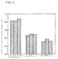
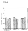
- the results of the surface roughness measurement and the results of the flatness measurement are also shown in FIGs. 1 and 2, respectively.
- Example 1 was repeated by using a different polishing agent containing 10 vol% of AJ-1325 specified above, and 90 vol% of pure water. The results of the surface roughness measurement and the results of the flatness measurement are also shown in FIGs. 1 and 2, respectively.
- the polished wafer surfaces obtained by using the colloidal silica polishing agent of Comparative Example 1 are comparable to those of Examples 1 and 2 in respect of the flatness. But, regarding the surface roughness, the polished wafer surfaces of Comparative Example 1 are much poorer than those of Examples 1 and 2.
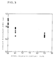
- Example 3 the condition specified above was changed such that the amount of Ethyl Silicate 28 was selected as 0 vol% for Comparative Example 2, 0.5 vol% for Example 3, and 2.5 vol% for Example 4.
- the pure water content was properly adjusted such that the total amount of the polishing agent was equal to 100 vol%.
- five sample wafers were polished and the polished sample wafers were measured for surface roughness in the same manner as Example 1.
- the results of the surface roughness measurement are shown in FIG. 3.
- the surface roughness is greatly improved by Ethyl Silicate 28 contained, as an additive, in the polishing agent. This is true for both Examples 3 and 4 having different Ethyl Silicate 28 contents.
- the same effect has been confirmed by experiments even when n-type wafers have been used in place of the p-type wafers used in the examples described above.
- a polishing agent of the present invention used in combination with a rigid polishing pad is able to provide, through a single-stage polishing process, a polished silicon wafer having an excellent flatness and whose surface has a roughness comparable to one obtained by the conventional final polishing process using a soft polishing pad.
- the present invention can obviate the use of the conventional final polishing process and hence is able to simplify the overall polishing process.
Landscapes
- Engineering & Computer Science (AREA)
- Mechanical Engineering (AREA)
- Chemical & Material Sciences (AREA)
- Organic Chemistry (AREA)
- Finish Polishing, Edge Sharpening, And Grinding By Specific Grinding Devices (AREA)
- Mechanical Treatment Of Semiconductor (AREA)
Applications Claiming Priority (2)
| Application Number | Priority Date | Filing Date | Title |
|---|---|---|---|
| JP12125094A JP2894208B2 (ja) | 1994-06-02 | 1994-06-02 | シリコンウェーハ研磨用研磨剤及び研磨方法 |
| JP121250/94 | 1994-06-02 |
Publications (2)
| Publication Number | Publication Date |
|---|---|
| EP0685877A2 true EP0685877A2 (de) | 1995-12-06 |
| EP0685877A3 EP0685877A3 (de) | 1997-01-08 |
Family
ID=14806619
Family Applications (1)
| Application Number | Title | Priority Date | Filing Date |
|---|---|---|---|
| EP95108481A Withdrawn EP0685877A3 (de) | 1994-06-02 | 1995-06-01 | Poliermittel zur Polierung von Siliziumscheiben und Verfahren zum Polieren unter Verwendung desselben. |
Country Status (3)
| Country | Link |
|---|---|
| US (1) | US5667567A (de) |
| EP (1) | EP0685877A3 (de) |
| JP (1) | JP2894208B2 (de) |
Cited By (7)
| Publication number | Priority date | Publication date | Assignee | Title |
|---|---|---|---|---|
| EP0779655A3 (de) * | 1995-12-14 | 1997-07-16 | International Business Machines Corporation | Verfahren zum chemisch-mechanischen Polieren eines Halbleitersubstrats eines elektronischen Bauteils |
| WO1997026114A1 (en) * | 1996-01-22 | 1997-07-24 | Micron Technology, Inc. | A polishing pad and a method for making a polishing pad with covalently bonded particles |
| EP0782179A3 (de) * | 1995-12-27 | 1997-07-30 | Shin-Etsu Handotai Co., Ltd | Verfahren zur Herstellung von spiegelblanken Halbleiter-Wafern |
| EP0750335A3 (de) * | 1995-06-23 | 1998-09-23 | Shin-Etsu Handotai Co., Ltd | Poliermittel zur Polierung von Halbleiterscheiben und Verfahren zum Polieren unter Verwendung derselben |
| US5938801A (en) * | 1997-02-12 | 1999-08-17 | Micron Technology, Inc. | Polishing pad and a method for making a polishing pad with covalently bonded particles |
| CN102382576A (zh) * | 2011-11-10 | 2012-03-21 | 江南大学 | 超声波雾化型碱性抛光液 |
| CN105462504A (zh) * | 2015-12-11 | 2016-04-06 | 蓝思科技(长沙)有限公司 | 一种c向蓝宝石抛光液及其制备方法 |
Families Citing this family (4)
| Publication number | Priority date | Publication date | Assignee | Title |
|---|---|---|---|---|
| GB2316414B (en) * | 1996-07-31 | 2000-10-11 | Tosoh Corp | Abrasive shaped article, abrasive disc and polishing method |
| KR100615691B1 (ko) | 1998-12-18 | 2006-08-25 | 도소 가부시키가이샤 | 연마용 부재, 그것을 이용한 연마용 정반 및 연마방법 |
| KR100637887B1 (ko) | 1998-12-28 | 2006-10-23 | 도소 가부시키가이샤 | 연마용 성형체, 이것을 이용한 연마용 정반 및 연마방법 |
| CN117067100A (zh) * | 2023-08-25 | 2023-11-17 | 济南晶正电子科技有限公司 | 晶圆及提高晶圆平整度的方法 |
Family Cites Families (13)
| Publication number | Priority date | Publication date | Assignee | Title |
|---|---|---|---|---|
| JPS598776A (ja) * | 1982-07-08 | 1984-01-18 | Toshiba Silicone Co Ltd | つや出し剤組成物 |
| SU1189668A1 (ru) * | 1983-10-05 | 1985-11-07 | Предприятие П/Я В-2998 | Масса дл изготовлени абразивного инструмента и способ его изготовлени |
| US4579564A (en) * | 1985-01-18 | 1986-04-01 | Smith Robert S | Polishing pad for a fine finish |
| SU1373551A1 (ru) * | 1986-07-01 | 1988-02-15 | Уральский филиал Всесоюзного научно-исследовательского института абразивов и шлифования | Способ изготовлени абразивного инструмента |
| SU1371891A1 (ru) * | 1986-08-25 | 1988-02-07 | Харьковский политехнический институт им.В.И.Ленина | Керамическа св зка дл изготовлени абразивного инструмента |
| JPS6374911A (ja) * | 1986-09-19 | 1988-04-05 | Shin Etsu Chem Co Ltd | 微細球状シリカの製造法 |
| US5226930A (en) * | 1988-06-03 | 1993-07-13 | Monsanto Japan, Ltd. | Method for preventing agglomeration of colloidal silica and silicon wafer polishing composition using the same |
| JPH029571A (ja) * | 1988-06-28 | 1990-01-12 | Fujitsu Ltd | 両面研磨方法 |
| US5352277A (en) * | 1988-12-12 | 1994-10-04 | E. I. Du Pont De Nemours & Company | Final polishing composition |
| JP2714411B2 (ja) * | 1988-12-12 | 1998-02-16 | イー・アイ・デュポン・ドゥ・ヌムール・アンド・カンパニー | ウェハーのファイン研摩用組成物 |
| JPH03108650A (ja) * | 1989-09-22 | 1991-05-08 | Seiko Epson Corp | 湿度センサ素子の製造方法 |
| JP3290189B2 (ja) * | 1991-04-11 | 2002-06-10 | 旭電化工業株式会社 | シリコンウェハーの研磨方法 |
| ATE120433T1 (de) * | 1991-05-28 | 1995-04-15 | Nalco Chemical Co | Polierbreie aus silika mit geringem gehalt an natrium und an metallen. |
-
1994
- 1994-06-02 JP JP12125094A patent/JP2894208B2/ja not_active Expired - Fee Related
-
1995
- 1995-06-01 EP EP95108481A patent/EP0685877A3/de not_active Withdrawn
-
1996
- 1996-12-16 US US08/755,802 patent/US5667567A/en not_active Expired - Fee Related
Non-Patent Citations (1)
| Title |
|---|
| None |
Cited By (11)
| Publication number | Priority date | Publication date | Assignee | Title |
|---|---|---|---|---|
| EP0750335A3 (de) * | 1995-06-23 | 1998-09-23 | Shin-Etsu Handotai Co., Ltd | Poliermittel zur Polierung von Halbleiterscheiben und Verfahren zum Polieren unter Verwendung derselben |
| US5866226A (en) * | 1995-06-23 | 1999-02-02 | Shin-Etsu Handotai Co., Ltd. | Polishing agent used for polishing semiconductor wafers and polishing method using the same |
| EP0779655A3 (de) * | 1995-12-14 | 1997-07-16 | International Business Machines Corporation | Verfahren zum chemisch-mechanischen Polieren eines Halbleitersubstrats eines elektronischen Bauteils |
| EP0782179A3 (de) * | 1995-12-27 | 1997-07-30 | Shin-Etsu Handotai Co., Ltd | Verfahren zur Herstellung von spiegelblanken Halbleiter-Wafern |
| US5821167A (en) * | 1995-12-27 | 1998-10-13 | Shin-Etsu Handotai Co., Ltd. | Method of manufacturing semiconductor mirror wafers |
| WO1997026114A1 (en) * | 1996-01-22 | 1997-07-24 | Micron Technology, Inc. | A polishing pad and a method for making a polishing pad with covalently bonded particles |
| US5823855A (en) * | 1996-01-22 | 1998-10-20 | Micron Technology, Inc. | Polishing pad and a method for making a polishing pad with covalently bonded particles |
| US5879222A (en) * | 1996-01-22 | 1999-03-09 | Micron Technology, Inc. | Abrasive polishing pad with covalently bonded abrasive particles |
| US5938801A (en) * | 1997-02-12 | 1999-08-17 | Micron Technology, Inc. | Polishing pad and a method for making a polishing pad with covalently bonded particles |
| CN102382576A (zh) * | 2011-11-10 | 2012-03-21 | 江南大学 | 超声波雾化型碱性抛光液 |
| CN105462504A (zh) * | 2015-12-11 | 2016-04-06 | 蓝思科技(长沙)有限公司 | 一种c向蓝宝石抛光液及其制备方法 |
Also Published As
| Publication number | Publication date |
|---|---|
| EP0685877A3 (de) | 1997-01-08 |
| US5667567A (en) | 1997-09-16 |
| JPH07326597A (ja) | 1995-12-12 |
| JP2894208B2 (ja) | 1999-05-24 |
Similar Documents
| Publication | Publication Date | Title |
|---|---|---|
| CN102049723B (zh) | 抛光半导体晶片的方法 | |
| US6352927B2 (en) | Semiconductor wafer and method for fabrication thereof | |
| EP0685877A2 (de) | Poliermittel zur Polierung von Siliziumscheiben und Verfahren zum Polieren unter Verwendung desselben | |
| EP0690772B1 (de) | Kompositionen und verfahren zum polieren und egalisieren von oberflächen | |
| JP3317330B2 (ja) | 半導体鏡面ウェーハの製造方法 | |
| JP5557506B2 (ja) | 半導体ウェーハの両面をポリッシングする方法 | |
| US5827395A (en) | Polishing pad used for polishing silicon wafers and polishing method using the same | |
| JP2004507085A (ja) | 新規な最終研磨方法を用いて半導体ウェーハを処理する方法および装置 | |
| EP0850724B1 (de) | Oberflächen-Schleifvorrichtung und Verfahren zum oberflächlichen Schleifen eines dünn-flächigen Werkstückes | |
| MY133700A (en) | Polishing fluid composition and polishing method | |
| EP0373501A3 (de) | Feine Polierzusammensetzung für Plaketten | |
| EP2365042A2 (de) | Polierzusammensetzung und Polierverfahren dafür | |
| TW376350B (en) | Process for polishing a semiconductor device substrate | |
| EP1566421A3 (de) | CMP Poliermittel, flüssiger Zusatz für CMP Poliermittel und Verfahren zum Polieren eines Substrates | |
| CN103846780A (zh) | 抛光半导体晶片的方法 | |
| JPWO2003070853A1 (ja) | 研磨スラリー | |
| US5891353A (en) | Polishing agent used for polishing semiconductor wafers and polishing method using the same | |
| EP1279713A1 (de) | Politurzusammensetzung und verfahren zur herstellung derselben sowie polierverfahren | |
| KR100792066B1 (ko) | 반도체 웨이퍼의 평탄화 가공방법 | |
| US6969304B2 (en) | Method of polishing semiconductor wafer | |
| JPH10329032A (ja) | Lsi酸化膜研磨用砥石およびlsi酸化膜研磨方法 | |
| JP3601937B2 (ja) | 表面平坦化方法および表面平坦化装置 | |
| JPH0319336A (ja) | 半導体ウェーハの研磨方法 | |
| JPH05337816A (ja) | シリコンウェーハの鏡面加工法 | |
| JPH03136766A (ja) | 半導体基板の研磨方法 |
Legal Events
| Date | Code | Title | Description |
|---|---|---|---|
| PUAI | Public reference made under article 153(3) epc to a published international application that has entered the european phase |
Free format text: ORIGINAL CODE: 0009012 |
|
| AK | Designated contracting states |
Kind code of ref document: A2 Designated state(s): DE FR GB |
|
| PUAL | Search report despatched |
Free format text: ORIGINAL CODE: 0009013 |
|
| AK | Designated contracting states |
Kind code of ref document: A3 Designated state(s): DE FR GB |
|
| 17P | Request for examination filed |
Effective date: 19970218 |
|
| STAA | Information on the status of an ep patent application or granted ep patent |
Free format text: STATUS: THE APPLICATION HAS BEEN WITHDRAWN |
|
| 18W | Application withdrawn |
Withdrawal date: 20020422 |