EP0687014B1 - Druckkontakt-Halbleitervorrichtung vom auf Licht ansprechenden Typ - Google Patents
Druckkontakt-Halbleitervorrichtung vom auf Licht ansprechenden Typ Download PDFInfo
- Publication number
- EP0687014B1 EP0687014B1 EP95104855A EP95104855A EP0687014B1 EP 0687014 B1 EP0687014 B1 EP 0687014B1 EP 95104855 A EP95104855 A EP 95104855A EP 95104855 A EP95104855 A EP 95104855A EP 0687014 B1 EP0687014 B1 EP 0687014B1
- Authority
- EP
- European Patent Office
- Prior art keywords
- semiconductor substrate
- pressure contact
- semiconductor device
- contact type
- type semiconductor
- Prior art date
- Legal status (The legal status is an assumption and is not a legal conclusion. Google has not performed a legal analysis and makes no representation as to the accuracy of the status listed.)
- Expired - Lifetime
Links
Images



Classifications
-
- H—ELECTRICITY
- H10—SEMICONDUCTOR DEVICES; ELECTRIC SOLID-STATE DEVICES NOT OTHERWISE PROVIDED FOR
- H10W—GENERIC PACKAGES, INTERCONNECTIONS, CONNECTORS OR OTHER CONSTRUCTIONAL DETAILS OF DEVICES COVERED BY CLASS H10
- H10W76/00—Containers; Fillings or auxiliary members therefor; Seals
- H10W76/10—Containers or parts thereof
- H10W76/12—Containers or parts thereof characterised by their shape
- H10W76/13—Containers comprising a conductive base serving as an interconnection
- H10W76/138—Containers comprising a conductive base serving as an interconnection having another interconnection being formed by a cover plate parallel to the conductive base, e.g. sandwich type
-
- G—PHYSICS
- G02—OPTICS
- G02B—OPTICAL ELEMENTS, SYSTEMS OR APPARATUS
- G02B6/00—Light guides; Structural details of arrangements comprising light guides and other optical elements, e.g. couplings
- G02B6/24—Coupling light guides
- G02B6/42—Coupling light guides with opto-electronic elements
- G02B6/4201—Packages, e.g. shape, construction, internal or external details
- G02B6/4204—Packages, e.g. shape, construction, internal or external details the coupling comprising intermediate optical elements, e.g. lenses, holograms
- G02B6/4212—Packages, e.g. shape, construction, internal or external details the coupling comprising intermediate optical elements, e.g. lenses, holograms the intermediate optical element being a coupling medium interposed therebetween, e.g. epoxy resin, refractive index matching material, index grease, matching liquid or gel
-
- G—PHYSICS
- G02—OPTICS
- G02B—OPTICAL ELEMENTS, SYSTEMS OR APPARATUS
- G02B6/00—Light guides; Structural details of arrangements comprising light guides and other optical elements, e.g. couplings
- G02B6/24—Coupling light guides
- G02B6/42—Coupling light guides with opto-electronic elements
- G02B6/4295—Coupling light guides with opto-electronic elements coupling with semiconductor devices activated by light through the light guide, e.g. thyristors, phototransistors
-
- H—ELECTRICITY
- H10—SEMICONDUCTOR DEVICES; ELECTRIC SOLID-STATE DEVICES NOT OTHERWISE PROVIDED FOR
- H10F—INORGANIC SEMICONDUCTOR DEVICES SENSITIVE TO INFRARED RADIATION, LIGHT, ELECTROMAGNETIC RADIATION OF SHORTER WAVELENGTH OR CORPUSCULAR RADIATION
- H10F30/00—Individual radiation-sensitive semiconductor devices in which radiation controls the flow of current through the devices, e.g. photodetectors
- H10F30/20—Individual radiation-sensitive semiconductor devices in which radiation controls the flow of current through the devices, e.g. photodetectors the devices having potential barriers, e.g. phototransistors
- H10F30/21—Individual radiation-sensitive semiconductor devices in which radiation controls the flow of current through the devices, e.g. photodetectors the devices having potential barriers, e.g. phototransistors the devices being sensitive to infrared, visible or ultraviolet radiation
- H10F30/26—Individual radiation-sensitive semiconductor devices in which radiation controls the flow of current through the devices, e.g. photodetectors the devices having potential barriers, e.g. phototransistors the devices being sensitive to infrared, visible or ultraviolet radiation the devices having three or more potential barriers, e.g. photothyristors
- H10F30/263—Photothyristors
-
- H—ELECTRICITY
- H10—SEMICONDUCTOR DEVICES; ELECTRIC SOLID-STATE DEVICES NOT OTHERWISE PROVIDED FOR
- H10F—INORGANIC SEMICONDUCTOR DEVICES SENSITIVE TO INFRARED RADIATION, LIGHT, ELECTROMAGNETIC RADIATION OF SHORTER WAVELENGTH OR CORPUSCULAR RADIATION
- H10F77/00—Constructional details of devices covered by this subclass
- H10F77/50—Encapsulations or containers
-
- H—ELECTRICITY
- H10—SEMICONDUCTOR DEVICES; ELECTRIC SOLID-STATE DEVICES NOT OTHERWISE PROVIDED FOR
- H10W—GENERIC PACKAGES, INTERCONNECTIONS, CONNECTORS OR OTHER CONSTRUCTIONAL DETAILS OF DEVICES COVERED BY CLASS H10
- H10W72/00—Interconnections or connectors in packages
-
- G—PHYSICS
- G02—OPTICS
- G02B—OPTICAL ELEMENTS, SYSTEMS OR APPARATUS
- G02B6/00—Light guides; Structural details of arrangements comprising light guides and other optical elements, e.g. couplings
- G02B6/24—Coupling light guides
- G02B6/42—Coupling light guides with opto-electronic elements
- G02B6/4201—Packages, e.g. shape, construction, internal or external details
- G02B6/4204—Packages, e.g. shape, construction, internal or external details the coupling comprising intermediate optical elements, e.g. lenses, holograms
- G02B6/421—Packages, e.g. shape, construction, internal or external details the coupling comprising intermediate optical elements, e.g. lenses, holograms the intermediate optical component consisting of a short length of fibre, e.g. fibre stub
-
- G—PHYSICS
- G02—OPTICS
- G02B—OPTICAL ELEMENTS, SYSTEMS OR APPARATUS
- G02B6/00—Light guides; Structural details of arrangements comprising light guides and other optical elements, e.g. couplings
- G02B6/24—Coupling light guides
- G02B6/42—Coupling light guides with opto-electronic elements
- G02B6/4201—Packages, e.g. shape, construction, internal or external details
- G02B6/4248—Feed-through connections for the hermetical passage of fibres through a package wall
Definitions
- the document EP 0 567 996 discloses another semiconductor device comprising a semiconductor element being held by external anode and cathode electrodes.
- the semiconductor element is brought into contact with the external anode and cathode electrodes through respective anode and cathode electrode plates under pressure.
- the cathode electrode plate has a through hole in its center while the external cathode electrode being provided with a hole in correspondence thereto, whereby an engaging hole is defined by the through hole and the hole.
- a gate electrode holder is slidably engaged in the engaging hole.
- the document EP EP-A-669652 which is with respect to the present invention a post-published prior art, discloses a pressure contact type semiconductor device comprising a semiconductor substrate being held between first and second distortion buffer plates which in turn being sandwiched by an anode flange and a cathode flange.
- the distortion buffer plates comprise respective through holes at the center.
- First and second bottomed holes are formed in the anode flange and the cathode flange.
- the housing is made airtight inside and inert gas is sealed therein.
- the end surface of the metal plate 8 silver-soldered to the main electrode 5 and the insulation tube 6 are welded at last, and the gas remaining inside is exhausted through the metal tube 11 and replaced by the inert gas, and then the end of the metal tube 11 is arc-welded to realize the airtightness of the housing and sealing of the inert gas.
- a pressure contact type semiconductor device comprises a semiconductor substrate, a thermal compensating plate in alloy-free contact with the semiconductor substrate, a main electrode in contact with the thermal compensating plate, wherein the thermal compensating plate and the main electrode fit to different ends of a pin to be positioned relatively to each other, both the thermal compensating plate and the main electrode having holes and the pin extends into the holes; the pressure contact type semiconductor device further comprising an insulation tube surrounding the semiconductor substrate, wherein the semiconductor substrate is fixed to an inner wall of the insulation tube, and a light guide transmitting a light signal to the semiconductor substrate, wherein a part of the light guide is accommodated in a tubular body and attached to the insulation tube.
- the main electrode and the thermal compensating plate in contact with each other fit to the common pin to be fixed, damage of the semiconductor substrate caused by displacement thereof in transportation and the like before use of the device can be prevented.
- the thermal compensating plate and the main electrode fit to the pin only at approximate center positions of the respective contact surfaces.
- the thermal compensating plate and the main electrode fit to the common pin only at a single position at the approximate center thereof, positional slipping off in the radial direction can be prevented with the simplest structure.
- the semiconductor substrate As the semiconductor substrate is fixed to the insulation tube, there is no possibility that the semiconductor substrate moves to abut on the inner wall of the insulation tube or the like to be damaged.
- the semiconductor substrate as the semiconductor substrate is fixed to the projection formed on the inner wall of the insulation tube, the semiconductor substrate can be easily fixed.
- the semiconductor substrate as the semiconductor substrate is fixed to the projection by using the adhesive agent, the semiconductor substrate can be fixed more easily.
- inside of the insulation tube accommodating the semiconductor substrate is airtight from outside and a through hole is formed in the projection.
- the semiconductor substrate in a pressure contact type semiconductor device is fixed to an inner wall of the insulation tube through a protection resin.
- the pressure contact type semiconductor device referring to the main electrode as a first main electrode comprises a second main electrode pressure-contacted to the semiconductor substrate from other side than the first one, and a control signal transmission path for transmitting a control signal to the semiconductor substrate, wherein the second main electrode defines a groove accommodating the control signal transmission path and the shape of the groove has its opening width increasing from a deeper portion toward an opening portion.
- the groove accommodating the control signal transmission path has a shape which has its width of opening increasing from the deeper portion toward the opening portion, such as a tapered shape, accommodation of the control signal transmission path is easy and the volume of the groove can be small. Accordingly, the loss heat produced in the semiconductor substrate can be effectively radiated to outside.
- the pressure contact type semiconductor device comprises a light guide transmitting a light signal to the semiconductor substrate, wherein a part of the light guide is accommodated in a tubular body and attached to the insulation tube.
- the pressure contact type semiconductor device comprises a light guide transmitting a light signal to the semiconductor substrate, wherein a part of the light guide is attached to the insulation tube through an elastic tubular body.
- the pressure contact type semiconductor device comprises a light guide transmitting a light signal to a light receiving surface of the semiconductor substrate and a guide ring fixed on the semiconductor substrate to surround the light receiving surface, wherein a light emitting end of the light guide is inserted into the guide ring.
- the light emitting end of the light guide can be easily positioned to an adequate position with respect to the light receiving surface.
- the pressure contact type semiconductor device refers to the guide ring as a first guide ring, and further comprises a second guide ring into which the light emitting end of the light guide is inserted, wherein the light emitting end of the light guide is inserted in the first guide ring with play and the second guide ring fits to the outer periphery of the first guide ring.
- the light emitting end of the light guide is fixed inside the guide ring by an adhesive optical coupling agent put inside the guide ring.
- the thermal stresses are absorbed by the optical coupling agent. Further, transmission of light signals from the light emitting end of the light guide to the light receiving surface of the semiconductor substrate can be made efficiently.
- the pressure contact type semiconductor device referring to the compensating plate and the main electrode respectively as first compensating plate and first main electrode, comprises a second thermal compensating plate in contact with the semiconductor substrate from other side than the firs one and a second main electrode in contact with the second thermal compensating plate, and a ring which fits to outer peripheries of both of the second thermal compensating plate and the second main electrode.
- Fig.1 is a front sectional view of a pressure contact type semiconductor device in the preferred embodiment.
- Fig.3 is a fragmentary enlarged front sectional view of the device in the preferred embodiment.
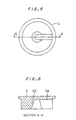
- Fig.5 is a front sectional view of the main electrode in the preferred embodiment.
- Fig.6 is a bottom view of the main electrode in the preferred embodiment.
- Fig.7 is an enlarged front sectional view of the vicinity of the light introducing window in the preferred embodiment.
- Fig.8 is an enlarged front sectional view of the vicinity of the light receiving surface in the preferred embodiment.
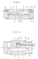
- Fig.9 is a front sectional view of a conventional pressure contact type semiconductor device.
- Fig.10 is a front sectional view of another conventional pressure contact type semiconductor device.
- Fig.1 is a front sectional view of a pressure contact type thyristor of the light trigger type in this preferred embodiment.
- a light receiving portion la is provided at the center portion of the upper main surface of the semiconductor substrate 1.
- a light emitting end of a light guide (control signal transmission path) 10 for transmitting light signals (control signals) inputted from outside faces to this light receiving portion 1a.
- thermal compensating plate 2 and a thermal compensating plate 3 abut on the upper main surface and the lower main surface of the semiconductor substrate 1, respectively.
- thermal compensating plates 2 and 3 are not alloyed to the semiconductor substrate 1 by soldering or the like, but they are pressure-contacted to the main surfaces of the semiconductor substrate 1 in the so-called alloy-free manner.
- the thermal compensating plates 2 and 3 are held between the main electrodes 4 and 5, respectively. These main electrodes 4 and 5 are fixed to an insulation tube 6 formed of ceramics, for example, through circular ring like metal plates 7 and 8, respectively.
- the insulation tube 6 has an outward projection, or a concave ⁇ co nvex portion for suppressing creeping discharge on its outer periphery.
- the insulation tube 6 also has a projection 6a projecting inwardly along its inner periphery.
- the thermal compensating plate 3 and the main electrode 5 are normally positioned by a screw pin (pin) 32. That is to say, a through hole is provided at the center of the thermal compensating plate 3 and a tapped hole is provided at the center of the corresponding main electrode 5, where the screw 32 which threadingly engages the tapped hole gets into the through hole of the thermal compensating plate 3 to restrict movement of the thermal compensating plate 3 in the radial direction.
- the thermal compensating plate 3 does not move in the radial direction, it does not give damage to the semiconductor substrate 1. Furthermore, it does not damage nor move insulation resin (resin for protection) 23, described later, attached to the outer periphery of the semiconductor substrate 1, either.
- the screw pin 32 threadingly engages the tapped hole of the main electrode 5 not to move in the axial direction of the through hole, so that it will not collide with the semiconductor substrate 1 to damage it. Also, the screw pin 32 prevents the movement in the radial direction in the thermal compensating plate 3 with the simplest structure of engaging only at the center portion of the thermal compensating plate 3 and the main electrode 5.
- FIG.2 and Fig.3 are fragmentary enlarged sectional views of the vicinity of the center part of the thermal compensating plate 3 shown in Fig.1.
- a hole having a bottom is provided in place of the through hole at the center of the thermal compensating plate 3, and a hole having a bottom similar to that of the thermal compensating plate 3 is provided in place of the tapped hole at the center of the corresponding main electrode 5.
- a pin 33 having no screw is used in place of the screw pin 32, and this pin 33 gets into the both holes having bottoms to realize normal position of the thermal compensating plate 3 and the main electrode 5.
- the movement of the thermal compensating plate 3 in the radial direction is also restricted, so it will not damage nor move the insulating resin 23 attached on the outer periphery of the semiconductor substrate 1. Furthermore, as the hole provided in the thermal compensating plate 3 is not a through hole but a hole having a bottom, the pin 33 will not hit the semiconductor substrate 1 to give damage to the semiconductor substrate 1.
- the fixing ring 30 is formed of resin or metal such as aluminum or the like.
- the main electrode 4 has a flange portion 4c projecting outwardly at the upper end of its outer peripheral surface.
- a spring (elastic body)31 such as a spring coil, a corrugated ring spring, or a belleville spring is interposed between the lower surface of this flange portion 4c and the upper end of the fixing ring 30.
- Restricting the movements of the semiconductor substrate 1 in the radial direction is also helpful in positioning the light emitting end of the light guide 10 and the light receiving portion la of the semiconductor substrate. That is to say, if the positions of the light emitting end of the light guide 10 and the light receiving portion la are registered and then they are bonded with the adhesive agent 24, errors in dimension among parts resulted from the dimensional tolerances of the light guide 10 or the like can be adjusted to realize precise positioning.
- Fig.4 is a plan view showing the semiconductor substrate 1 fixed to the projection 6a.
- the adhesive agent 24 is applied at intervals around the semiconductor substrate 1.
- through holes 6b passing through from the upper surface to the lower surface of the projection 6a are provided at the positions where the adhesive agent 24 is not applied to.
- this establishes communication between above and below the semiconductor substrate 1.
- the gases such as the oxidizing gas, steam, and the like produced in the housing can be exhausted through the exhaust spigot 11b provided above the semiconductor substrate 1, and further the gas in the housing can be replaced by the inert gas.
- notches (grooves) 4a and 4b for introducing the light guide 10 are formed in the main electrode 4.
- the loss heat generated in the semiconductor substrate 1 is transmitted through the main electrodes 4 and 5 and radiated out of the device.
- the volume of the cavity formed in the main electrode 4 by the notches 4a and 4b is as small as possible.
- Fig.5 and Fig.6 which are respectively a sectional view and a bottom view of the main electrode 4
- the shape of the notch 4b at the center of the main electrode 4 is not a cylindrical shape but a frustum of a cone, i.e., it is tapered.
- the shape of the notch 4b may be a hemisphere in place of a frustum of a cone, or it may take other shapes which have its opening area increasing as it gets closer to the bottom. Though not shown in the figure, the shape of the notch 4a is also preferably set so that it becomes larger as it gets closer to the opening away from the bottom of the groove.
- Fig.7 is an enlarged front sectional view of the vicinity of the horizontal light entering end in the light guide 10 which bends in the form of "L".
- a through hole for transmitting the light signals is formed in the horizontal direction in the insulation tube 6.
- a metal tube 40 is fixedly inserted in this through hole.
- An optical transmissive light introducing window 42 through which light signals from outside are transmitted is airtightly bonded to this metal tube 40 through a circular ring like fixing jig 41.
- a tubular body 43 threadingly engages the inner side of the metal tube 40 to be fixedly inserted therethrough.
- the tubular body 43 is formed of resin or metal, for example, with its inside diameter somewhat larger than the diameter of the light guide 10 so that they are not in contact with each other.
- the tubular body 43 projects more inwardly than the inner side of the insulation tube 6. Even if the main electrode 4 in Fig.1 turns in the assembling work before welding, the notch 4a will not directly abut on the light guide 10 because of the existence of the tubular body 43. That is, the tubular body 43 serves as a protection member for protecting the light guide 10.
- the light guide 10 is flexibly supported by the metal tube 40 with this elastic tubular body 44 interposed therebetween. Accordingly, vibration, impact and the like applied from outside are absorbed by the elastic tubular body 44, and the light guide 10 is prevented from being damaged by the vibrations, impact, etc.
- a reflection preventing film formed of silicon dioxide, for example, having a single layer or multiple layers is formed on the both surfaces of the light introducing window 42 by a method of vapor deposition or the like. This suppresses reflection of light signals which will cause transmission loss of light signals and improves the transmission efficiency.
- a material which can satisfactorily stand high temperature when soldered is selected for the reflection preventing film, since the formation of the reflection preventing film is performed before the light introducing window 42 is fixed to the fixing jig 41 by soldering or the like.
- a similar reflection preventing film is formed on both of the light entering end and the light emitting end of the light guide 10 or on one of them to improve the transmission efficiency of light signals.
- Fig.8 is an enlarged front sectional view in the vicinity of the light emitting end of the light guide 10.
- Two guide rings 50 and 51 are used to normally position the light emitting end of the light guide 10 to the light receiving portion la of the semiconductor substrate 1.
- the guide rings 50 and 51 are formed of resin or the like.
- the guide ring 50 has a through hole formed at its center, into which the light guide 10 is inserted. Furthermore, the guide ring 50 fits to the outer periphery of the guide ring 51.
- the guide ring 51 is first provided at a position concentric with the light receiving portion la of the semiconductor substrate 1 and then it is fixed with adhesive agent 52. After that, optical coupling agent 20 is put inside the guide ring 51. Resin which has some fluidity before solidifying and maintains some flexibility after thermally treated or left at ordinary temperature and solidified, and which has optical transparency and refractive index of about 1.3 to 1.5 is selected for the optical coupling agent 20. Silicone rubber system is suitable for this, for example.
- the light emitting end of the light guide 10 is inserted into the optical coupling agent 20 and the guide ring 50 with the light guide 10 previously inserted therein is fitted to the guide ring 51.
- the guide ring 51 is fixed at the predetermined position, the light emitting end of the light guide 10 is naturally positioned above the light receiving portion 1a when the guide rings 50 and 51 fit to each other. Accordingly, light signals are surely transmitted to the light receiving portion 1a of the semiconductor substrate 1.
- the optical coupling agent 20 has the flexibility, the expansion and shrinkage of the parts such as the light guide 10 due to the temperature cycle are absorbed by the optical coupling agent 20. Accordingly, damage or the like of the light guide 10 caused by the thermal stresses resulted from the temperature cycle is prevented.
Landscapes
- Physics & Mathematics (AREA)
- General Physics & Mathematics (AREA)
- Optics & Photonics (AREA)
- Thyristors (AREA)
- Die Bonding (AREA)
Claims (21)
- Druckkontakt-Halbleitervorrichtung, mit:einem Halbleitersubstrat (1), einer Wärmeausgleichsplatte (3) in legierungsfreiem Kontakt mit dem Halbleitersubstrat (1), einer mit der Wärmeausgleichsplatte (3) in Kontakt stehenden Hauptelektrode (5), worin die Wärmeausgleichsplatte (3) und die Hauptelektrode (5) an verschiedenen Endabschnitten eines Stiftes (32) angebracht sind, so daß sie in Bezug zueinander positioniert sind, wobei die Wärmeausgleichsplatte (3) und die Hauptelektrode (5) Löcher haben und sich der Stift (32) in die Löcher erstreckt;einem Isolierrohr (6), das das Halbleitersubstrat (1) umgibt, worin das Halbleitersubstrat (1) an einer Innenwandung des Isolierrohres (6) angebracht ist; undeinem Lichtleiter (10), der ein Lichtsignal zu dem Halbleitersubstrat (1) überträgt, worin ein Teil des Lichtleiters (10) in einem rohrförmigen Körper (43) angeordnet und an dem Isolierrohr (6) angebracht ist.
- Druckkontakt-Halbleitervorrichtung nach Anspruch 1, worin die Wärmeausgleichsplatte (3) und die Hauptelektrode (5) an dem Stift (32) nur an ungefähr mittigen Positionen von jeweiligen Kontaktflächen angebracht sind.
- Druckkontakt-Halbleitervorrichtung nach Anspruch 1, worin an der Innenwandung des Isolierrohres (6) ein nach innen hervorstehender Vorsprung (6a) ausgeformt ist und worin das Halbleitersubstrat (1) an dem Vorsprung (6a) angebracht ist.
- Druckkontakt-Halbleitervorrichtung nach Anspruch 3, worin das Halbleitersubstrat (1) an dem Vorsprung (6a) unter Verwendung eines Klebemittels (24) angebracht ist.
- Druckkontakt-Halbleitervorrichtung nach Anspruch 3, worin das Halbleitersubstrat (1) an dem Vorsprung (6a) durch ein Schutzharz (23) angebracht ist, das an dem Außenumfang des Substrates vorgesehen ist.
- Druckkontakt-Halbleitervorrichtung nach Anspruch 3, worin der Vorsprung (6a) an dem gesamten Umfang der Innenwandung ausgeformt ist.
- Druckkontakt-Halbleitervorrichtung nach Anspruch 6, worin das Innere des Isolierrohres (6), das das Halbleitersubstrat (1) aufnimmt, zur Außenseite luftdicht ist und worin in dem Vorsprung (6a) ein Durchgangsloch (6b) ausgeformt ist.
- Druckkontakt-Halbleitervorrichtung nach Anspruch 1, worin das Halbleitersubstrat (1) an der Innenwandung des Isolierrohres (6) durch ein Schutzharz (23) angebracht ist.
- Druckkontakt-Halbleitervorrichtung nach einem der Ansprüche 1 bis 8, wobei die Hauptelektrode (5) als eine erste Hauptelektrode bezeichnet wird und wobei die Vorrichtung außerdem aufweist eine zweite Hauptelektrode (4), die an dem Halbleitersubstrat (1) von einer anderen Seite als die erste Hauptelektrode durch Druck in Kontakt steht, und eine Steuersignalübertragungsweg (10) zum Übertragen eines Steuersignales zu dem Halbleitersubstrat (1), worin die zweite Hauptelektrode (4) eine Ausnehmung (4a, 4b) bildet, die den Steuersignalübertragungsweg (10) aufnimmt und worin eine Form der Ausnehmung (4a, 4b) eine derartige Öffnungsbreite hat, daß sich diese von einem tieferen Abschnitt zu einem Öffnungsabschnitt hin vergrößert.
- Druckkontakt-Halbleitervorrichtung nach Anspruch 1, worin der rohrförmige Körper (43) mit der Innenseite eines Metallrohres (40) in Eingriff steht, das in ein Durchgangsloch in dem Isolierrohr (6) fest eingefügt ist.
- Druckkontakt-Halbleitervorrichtung nach Anspruch 1, worin der rohrförmige Körper (43) innerhalb des Isolierrohres (6) hervorsteht und worin der Lichtleiter (10) in den rohrförmigen Körper (43) mit Spiel eingefügt ist.
- Druckkontakt-Halbleitervorrichtung nach Anspruch 1, worin ein Teil des Lichtleiters (10) durch einen elastischen rohrförmigen Körper (44) in den rohrförmigen Körper (43) eingefügt ist.
- Druckkontakt-Halbleitervorrichtung nach Anspruch 1, worin ein Teil des Lichtleiters (10) durch einen elastischen, rohrförmigen Körper (44) an dem Isolierrohr (6) angebracht ist.
- Druckkontakt-Halbleitervorrichtung nach einem der Ansprüche 1 bis 13, worin der Lichtleiter (10) zu einer Lichtaufnahmefläche (la) des Halbleitersubstrates (1) ein Lichtsignal überträgt und worin die Vorrichtung außerdem einen Führungsring (51) aufweist, der an dem Halbleitersubstrat (1) derart angebracht ist, daß er die Lichtaufnahmefläche (la) umgibt, worin ein Lichtaustrittsendabschnitt des Lichtleiters (10) in den Führungsring (51) eingefügt ist.
- Druckkontakt-Halbleitervorrichtung nach Anspruch 14, wobei der Führungsring (51) als ein erster Führungsring bezeichnet wird, und wobei die Vorrichtung außerdem einen zweiten Führungsring (50) aufweist, in welchen der Lichtaustrittsendabschnitt des Lichtleiters (10) eingefügt ist, worin der Lichtaustrittsendabschnitt des Lichtleiters (10) in den ersten Führungsring (51) mit Spiel eingefügt ist und worin der zweite Führungsring (50) an dem Außenumfang des ersten Führungsringes (51) angebracht ist.
- Druckkontakt-Halbleitervorrichtung nach Anspruch 14, worin der Lichtaustrittsendabschnitt des Lichtleiters (10) innerhalb des Führungsringes (51) durch ein optisches Klebemittel (20) angebracht ist, das in den Führungsring (51) eingebracht ist.
- Druckkontakt-Halbleitervorrichtung nach einem der Ansprüche 1 bis 8, wobei die Ausgleichsplatte (3) und die Hauptelektrode (5) jeweils als erste Ausgleichsplatte und als erste Hauptelektrode bezeichnet werden und wobei die Vorrichtung außerdem aufweist eine zweite Wärmeausgleichsplatte (2), die mit dem Halbleitersubstrat (1) von einer anderen Seite als der ersten Seite in Kontakt steht, eine zweite, mit der zweiten Wärmeausgleichsplatte (2) in Kontakt stehende Hauptelektrode (4) und einen Ring (30), der an den Außenumfängen von der zweiten Wärmeausgleichsplatte (2) und der zweiten Hauptelektrode (4) angebracht ist.
- Druckkontakt-Halbleitervorrichtung nach Anspruch 17, die außerdem einen elastischen Körper (31) aufweist, der zwischen der zweiten Hauptelektrode (4) und dem Ring (30) angeordnet ist, worin der Ring (30) mit einem Kantenabschnitt einer Oberfläche der zweiten Wärmeausgleichsplatte (2) in Eingriff steht, die an die zweite Hauptelektrode (4) anstößt, und worin der Ring (30) durch eine elastische Kraft des elastischen Körpers (31) gegen die zweite Wärmeausgleichsplatte (2) gedrückt und unter Spannung gesetzt wird.
- Druckkontakt-Halbleitervorrichtung nach Anspruch 1, worin sich der Stift (32, 33) in die Löcher eng mit minimalem Spiel erstreckt.
- Druckkontakt-Halbleitervorrichtung nach einem der Ansprüche 1 bis 19, worin der Stift (32, 33) in Form eines geraden Kreiszylinders ausgeformt ist.
- Druckkontakt-Halbleitervorrichtung nach einem der Ansprüche 1, 19 und 20, worin sich die Wärmeausgleichsplatte (3) mit dem Halbleitersubstrat (1) auf einer Seite davon, mit der ein Steuersignalübertragungsweg (10) zum Übertragen eines Steuersignales nicht in Kontakt steht, in legierungsfreiem Kontakt befindet.
Applications Claiming Priority (3)
| Application Number | Priority Date | Filing Date | Title |
|---|---|---|---|
| JP7312894 | 1994-04-12 | ||
| JP73128/94 | 1994-04-12 | ||
| JP07312894A JP3469304B2 (ja) | 1994-04-12 | 1994-04-12 | 半導体装置 |
Publications (3)
| Publication Number | Publication Date |
|---|---|
| EP0687014A2 EP0687014A2 (de) | 1995-12-13 |
| EP0687014A3 EP0687014A3 (de) | 1996-05-01 |
| EP0687014B1 true EP0687014B1 (de) | 1999-11-24 |
Family
ID=13509278
Family Applications (1)
| Application Number | Title | Priority Date | Filing Date |
|---|---|---|---|
| EP95104855A Expired - Lifetime EP0687014B1 (de) | 1994-04-12 | 1995-03-31 | Druckkontakt-Halbleitervorrichtung vom auf Licht ansprechenden Typ |
Country Status (4)
| Country | Link |
|---|---|
| US (2) | US5621237A (de) |
| EP (1) | EP0687014B1 (de) |
| JP (1) | JP3469304B2 (de) |
| DE (1) | DE69513447T2 (de) |
Families Citing this family (10)
| Publication number | Priority date | Publication date | Assignee | Title |
|---|---|---|---|---|
| DE19626661A1 (de) * | 1996-07-03 | 1998-01-08 | Asea Brown Boveri | Lichtzündbarer Leistungshalbleiter |
| DE19627426A1 (de) * | 1996-07-08 | 1998-01-15 | Asea Brown Boveri | Lichtzündbarer Leistungshalbleiter sowie Verfahren zum Zusammenbauen eines solchen lichtzündbaren Leistungshalbleiters |
| JP3571354B2 (ja) * | 1999-01-18 | 2004-09-29 | 三菱電機株式会社 | 圧接型半導体装置 |
| US7861712B2 (en) * | 2004-04-23 | 2011-01-04 | Manta Product Development | Sealed capsule including an integrated puncturing mechanism |
| DE102009034138B4 (de) * | 2009-07-22 | 2011-06-01 | Semikron Elektronik Gmbh & Co. Kg | Leistungshalbleitermodul mit einem Sandwich mit einem Leistungshalbleiterbauelement |
| US8631878B2 (en) * | 2010-01-21 | 2014-01-21 | Vetco Gray Inc. | Wellhead annulus seal assembly and method of using same |
| US8668021B2 (en) | 2010-10-26 | 2014-03-11 | Vetco Gray Inc. | Energizing ring nose profile and seal entrance |
| GB2529338B (en) * | 2013-05-13 | 2019-03-20 | Abb Schweiz Ag | Spacer system for a semiconductor switching device |
| JP2016062983A (ja) * | 2014-09-16 | 2016-04-25 | 株式会社東芝 | 半導体装置 |
| CN109494206B (zh) * | 2017-09-12 | 2022-05-24 | 株洲中车时代半导体有限公司 | 一种晶闸管 |
Citations (2)
| Publication number | Priority date | Publication date | Assignee | Title |
|---|---|---|---|---|
| JPS63128650A (ja) * | 1986-11-19 | 1988-06-01 | Hitachi Ltd | 加圧接触形半導体装置 |
| EP0567996A1 (de) * | 1992-04-28 | 1993-11-03 | Mitsubishi Denki Kabushiki Kaisha | Halbleiteranordnung und Verfahren zum Zusammensetzen derselben |
Family Cites Families (16)
| Publication number | Priority date | Publication date | Assignee | Title |
|---|---|---|---|---|
| JPS5629351A (en) * | 1979-08-20 | 1981-03-24 | Toshiba Corp | Semiconductor device |
| JPS5949709B2 (ja) * | 1979-10-13 | 1984-12-04 | 三菱電機株式会社 | 光点弧サイリスタ装置 |
| JPS57143849A (en) * | 1981-03-02 | 1982-09-06 | Toshiba Corp | Flat semiconductor element |
| EP0064383A3 (de) * | 1981-05-06 | 1984-06-27 | LUCAS INDUSTRIES public limited company | Ein Halbleitergehäuse |
| JPS58207644A (ja) * | 1982-05-29 | 1983-12-03 | Toshiba Corp | 半導体装置 |
| JPS58215041A (ja) * | 1982-06-09 | 1983-12-14 | Hitachi Ltd | 半導体装置 |
| JPS5921062A (ja) * | 1982-07-26 | 1984-02-02 | Mitsubishi Electric Corp | サイリスタ |
| JPS59200441A (ja) * | 1983-04-27 | 1984-11-13 | Mitsubishi Electric Corp | 半導体素子 |
| JPS59231858A (ja) * | 1983-06-13 | 1984-12-26 | Mitsubishi Electric Corp | 光駆動半導体装置 |
| JPS6042875A (ja) * | 1983-08-17 | 1985-03-07 | Mitsubishi Electric Corp | 受光素子 |
| JPS60194565A (ja) * | 1984-03-15 | 1985-10-03 | Mitsubishi Electric Corp | 半導体装置 |
| JPS63289940A (ja) * | 1987-05-22 | 1988-11-28 | Fuji Electric Co Ltd | 半導体装置 |
| GB8928492D0 (en) * | 1989-12-18 | 1990-02-21 | Westinghouse Brake & Signal | Housings for semiconductor devices |
| JPH03219675A (ja) * | 1990-01-25 | 1991-09-27 | Hitachi Ltd | 光駆動半導体装置 |
| JPH04129232A (ja) * | 1990-09-19 | 1992-04-30 | Mitsubishi Electric Corp | 圧接型半導体装置 |
| DE4227063A1 (de) * | 1992-08-15 | 1994-02-17 | Abb Research Ltd | Abschaltbares Hochleistungs-Halbleiterbauelement |
-
1994
- 1994-04-12 JP JP07312894A patent/JP3469304B2/ja not_active Expired - Lifetime
-
1995
- 1995-03-21 US US08/407,637 patent/US5621237A/en not_active Expired - Lifetime
- 1995-03-31 EP EP95104855A patent/EP0687014B1/de not_active Expired - Lifetime
- 1995-03-31 DE DE69513447T patent/DE69513447T2/de not_active Expired - Lifetime
-
1996
- 1996-11-12 US US08/746,415 patent/US5801429A/en not_active Expired - Lifetime
Patent Citations (2)
| Publication number | Priority date | Publication date | Assignee | Title |
|---|---|---|---|---|
| JPS63128650A (ja) * | 1986-11-19 | 1988-06-01 | Hitachi Ltd | 加圧接触形半導体装置 |
| EP0567996A1 (de) * | 1992-04-28 | 1993-11-03 | Mitsubishi Denki Kabushiki Kaisha | Halbleiteranordnung und Verfahren zum Zusammensetzen derselben |
Also Published As
| Publication number | Publication date |
|---|---|
| JPH07283250A (ja) | 1995-10-27 |
| US5801429A (en) | 1998-09-01 |
| DE69513447D1 (de) | 1999-12-30 |
| EP0687014A3 (de) | 1996-05-01 |
| JP3469304B2 (ja) | 2003-11-25 |
| US5621237A (en) | 1997-04-15 |
| DE69513447T2 (de) | 2000-07-06 |
| EP0687014A2 (de) | 1995-12-13 |
Similar Documents
| Publication | Publication Date | Title |
|---|---|---|
| US6821030B2 (en) | Optical coupling apparatus | |
| EP0053020B1 (de) | Lichtempfindliche Halbleitervorrichtung | |
| CN101986179B (zh) | 半导体器件组件 | |
| US6786627B2 (en) | Light generating module | |
| US20100272393A1 (en) | Wafer based optical chassis and associated methods | |
| US5801429A (en) | Semiconductor device | |
| US20130215924A1 (en) | Non-hermetic, multi-emitter laser pump packages and methods for forming the same | |
| JPH10190141A (ja) | 光半導体モジュール | |
| US5596210A (en) | Light trigger type semiconductor device with reflection prevention film | |
| US6843609B2 (en) | Optical module with lens holding member | |
| EP0911923B1 (de) | Halbleiterlasermodul | |
| EP4160705B1 (de) | Lichtwellenleitergehäuse und lichtemittierende vorrichtung | |
| JP2616671B2 (ja) | 光学モジュール装置 | |
| JP3560571B2 (ja) | 半導体装置 | |
| US20220329323A1 (en) | Optical emitting device with built-in thermoelectric cooler and optical transceiver module having the same | |
| JP4009110B2 (ja) | 光半導体素子収納用パッケージおよび光半導体装置 | |
| WO2022246374A1 (en) | Heatsinking in laser devices | |
| US20250385142A1 (en) | Housing Packaging Structure, Packaging Assembly, and Electronic Device | |
| JPH11289038A (ja) | 電子温度調整装置 | |
| US20240272379A1 (en) | Optical waveguide package and light-emitting device | |
| JPH06140673A (ja) | 光素子の実装法 | |
| KR100784943B1 (ko) | 열전 냉각기를 구비하는 레이저 다이오드 광모듈 | |
| JP2009014935A (ja) | 光通信用パッケージ | |
| JPS6148787B2 (de) | ||
| JP3881574B2 (ja) | 光半導体素子収納用パッケージ |
Legal Events
| Date | Code | Title | Description |
|---|---|---|---|
| PUAI | Public reference made under article 153(3) epc to a published international application that has entered the european phase |
Free format text: ORIGINAL CODE: 0009012 |
|
| AK | Designated contracting states |
Kind code of ref document: A2 Designated state(s): CH DE GB LI |
|
| PUAL | Search report despatched |
Free format text: ORIGINAL CODE: 0009013 |
|
| AK | Designated contracting states |
Kind code of ref document: A3 Designated state(s): CH DE GB LI |
|
| 17P | Request for examination filed |
Effective date: 19960521 |
|
| 17Q | First examination report despatched |
Effective date: 19961115 |
|
| GRAG | Despatch of communication of intention to grant |
Free format text: ORIGINAL CODE: EPIDOS AGRA |
|
| GRAG | Despatch of communication of intention to grant |
Free format text: ORIGINAL CODE: EPIDOS AGRA |
|
| GRAH | Despatch of communication of intention to grant a patent |
Free format text: ORIGINAL CODE: EPIDOS IGRA |
|
| GRAH | Despatch of communication of intention to grant a patent |
Free format text: ORIGINAL CODE: EPIDOS IGRA |
|
| GRAA | (expected) grant |
Free format text: ORIGINAL CODE: 0009210 |
|
| AK | Designated contracting states |
Kind code of ref document: B1 Designated state(s): CH DE GB LI |
|
| REG | Reference to a national code |
Ref country code: CH Ref legal event code: EP |
|
| REF | Corresponds to: |
Ref document number: 69513447 Country of ref document: DE Date of ref document: 19991230 |
|
| REG | Reference to a national code |
Ref country code: CH Ref legal event code: NV Representative=s name: BOVARD AG PATENTANWAELTE |
|
| PLBE | No opposition filed within time limit |
Free format text: ORIGINAL CODE: 0009261 |
|
| STAA | Information on the status of an ep patent application or granted ep patent |
Free format text: STATUS: NO OPPOSITION FILED WITHIN TIME LIMIT |
|
| 26N | No opposition filed | ||
| REG | Reference to a national code |
Ref country code: GB Ref legal event code: IF02 |
|
| REG | Reference to a national code |
Ref country code: GB Ref legal event code: 746 Effective date: 20020305 |
|
| REG | Reference to a national code |
Ref country code: CH Ref legal event code: PFA Owner name: MITSUBISHI DENKI KABUSHIKI KAISHA Free format text: MITSUBISHI DENKI KABUSHIKI KAISHA#2-3, MARUNOUCHI 2-CHOME CHIYODA-KU#TOKYO 100 (JP) -TRANSFER TO- MITSUBISHI DENKI KABUSHIKI KAISHA#2-3, MARUNOUCHI 2-CHOME CHIYODA-KU#TOKYO 100 (JP) |
|
| PGFP | Annual fee paid to national office [announced via postgrant information from national office to epo] |
Ref country code: CH Payment date: 20140312 Year of fee payment: 20 |
|
| PGFP | Annual fee paid to national office [announced via postgrant information from national office to epo] |
Ref country code: GB Payment date: 20140326 Year of fee payment: 20 |
|
| PGFP | Annual fee paid to national office [announced via postgrant information from national office to epo] |
Ref country code: DE Payment date: 20140417 Year of fee payment: 20 |
|
| REG | Reference to a national code |
Ref country code: DE Ref legal event code: R071 Ref document number: 69513447 Country of ref document: DE |
|
| REG | Reference to a national code |
Ref country code: CH Ref legal event code: PL |
|
| REG | Reference to a national code |
Ref country code: GB Ref legal event code: PE20 Expiry date: 20150330 |
|
| PG25 | Lapsed in a contracting state [announced via postgrant information from national office to epo] |
Ref country code: GB Free format text: LAPSE BECAUSE OF EXPIRATION OF PROTECTION Effective date: 20150330 |