EP0689363A2 - Digitale Konvergenzvorrichtung - Google Patents
Digitale Konvergenzvorrichtung Download PDFInfo
- Publication number
- EP0689363A2 EP0689363A2 EP95304367A EP95304367A EP0689363A2 EP 0689363 A2 EP0689363 A2 EP 0689363A2 EP 95304367 A EP95304367 A EP 95304367A EP 95304367 A EP95304367 A EP 95304367A EP 0689363 A2 EP0689363 A2 EP 0689363A2
- Authority
- EP
- European Patent Office
- Prior art keywords
- convergence
- data
- correction
- memory
- horizontal
- Prior art date
- Legal status (The legal status is an assumption and is not a legal conclusion. Google has not performed a legal analysis and makes no representation as to the accuracy of the status listed.)
- Withdrawn
Links
- 238000012937 correction Methods 0.000 claims abstract description 415
- 230000015654 memory Effects 0.000 claims abstract description 173
- 230000003068 static effect Effects 0.000 claims abstract description 143
- 230000004044 response Effects 0.000 claims description 13
- 238000010586 diagram Methods 0.000 description 24
- 238000010276 construction Methods 0.000 description 16
- 238000012546 transfer Methods 0.000 description 14
- 238000013500 data storage Methods 0.000 description 12
- 238000010894 electron beam technology Methods 0.000 description 10
- 230000008859 change Effects 0.000 description 4
- 230000000694 effects Effects 0.000 description 4
- 230000005389 magnetism Effects 0.000 description 4
- 230000003287 optical effect Effects 0.000 description 4
- 230000008901 benefit Effects 0.000 description 3
- 238000009125 cardiac resynchronization therapy Methods 0.000 description 3
- 238000012545 processing Methods 0.000 description 3
- 239000003086 colorant Substances 0.000 description 2
- 238000009434 installation Methods 0.000 description 2
- 238000004519 manufacturing process Methods 0.000 description 2
- 238000012986 modification Methods 0.000 description 2
- 230000004048 modification Effects 0.000 description 2
- 230000003111 delayed effect Effects 0.000 description 1
- 230000002542 deteriorative effect Effects 0.000 description 1
- 238000011161 development Methods 0.000 description 1
- 230000014759 maintenance of location Effects 0.000 description 1
- 239000000463 material Substances 0.000 description 1
- 230000001737 promoting effect Effects 0.000 description 1
- 230000000717 retained effect Effects 0.000 description 1
- 239000003381 stabilizer Substances 0.000 description 1
- 238000004804 winding Methods 0.000 description 1
Images


Classifications
-
- H—ELECTRICITY
- H04—ELECTRIC COMMUNICATION TECHNIQUE
- H04N—PICTORIAL COMMUNICATION, e.g. TELEVISION
- H04N9/00—Details of colour television systems
- H04N9/12—Picture reproducers
- H04N9/31—Projection devices for colour picture display, e.g. using electronic spatial light modulators [ESLM]
-
- H—ELECTRICITY
- H04—ELECTRIC COMMUNICATION TECHNIQUE
- H04N—PICTORIAL COMMUNICATION, e.g. TELEVISION
- H04N9/00—Details of colour television systems
- H04N9/12—Picture reproducers
- H04N9/16—Picture reproducers using cathode ray tubes
- H04N9/28—Arrangements for convergence or focusing
Definitions
- the present invention relates to a digital convergence apparatus which is used in color television receivers, and R, G and B three-tube type projection television receivers.
- the projection type color television receivers are so structured that a picture from projection tubes (CRT) is projected after magnified through a lens system, they can be designed relatively compact in size and light in weight. So, the projection type has now become the mainstream in color television receivers in size larger than 40''.
- the projection type color television receiver has monochrome projection picture tubes of R (red), G (green) and B (blue).
- the video signals in R (red), G (green) and B (blue) are then supplied to respective projection tubes which are aligned in a line.
- R, G and B images on respective projection tubes are magnified, projected and imaged on a screen through an optical system comprising lenses, reflectors, etc.
- some color deviations are induced in the projected image on the screen due to the different angles of incidence of beams emitted from respective projection tubes onto the screen, an alignment deviation of the three monochrome projection tubes, unmatching of orbits of the electron beams due to the earth magnetism, etc.
- a convergence correction apparatus is provided to focuses R, G and B image electron beams on the screen by correcting the deviation angles of the electron beams by applying the correction field through the convergence correction coil provided to the projection tube of each axis.
- FIGURE 8 is an explanatory diagram showing one example of such conventional projection type television receiver
- FIGURE 9 is an explanatory diagram showing the arrangement of R, G and B projection tubes in such conventional projection type television receiver.
- FIGURE 8 a screen 2 is provided on the upper front side in a cabinet 1.
- a chassis (not shown) is installed on the floor of the cabinet 1, and then an image receiving circuit (not shown), etc, are mounted on the chassis.
- supporting members (not shown) are mounted within the cabinet 1, so as that the R, G and B projection tubes 3R, 3G and 3B are installed in the cabinet 1 by being supported on these supporting members.
- R, G and B image electron beams are thus emitted from the R, G and B projection tubes 3R, 3G and 3B in response to the image signals provided from the image receiving circuit.
- the image electron beams emitted from the projection tubes 3R, 3G and 3B are reflected by a reflection mirror 4 mounted on the front surface of the cabinet 1 as well as a reflection mirror 5 mounted on the rear surface through projection lens 6R, 6G and 6B, respectively, thus projected on the screen 2.
- FIGURE 9 shows the orientations of the projection tubes 3R, 3G and 3B viewed from the top of the cabinet 1.
- the R, G and B projection tubes 3R, 3G and 3B are aligned in a horizontal line parallel to the screen 2, as shown in FIGURE 9. Further, the projection tubes 3R, 3G and 3B are so arranged that their optical axes join to each other in consideration of the structure of the optical system.
- the R, G and B image electron beams from the projection tubes 3R, 3G and 3B are emitted through respective projection lenses 6R, 6G and 6B to form images on the screen 2. A magnified color image is thus displayed on the screen.
- FIGURE 10 is a block diagram showing a color television receiver with such a conventional digital convergence apparatus.
- FIGURE 10 only the R image section is shown but other G and B image sections are also in the same structure as the R image section.
- the apparatus as shown in FIGURE 10 forms an image of a convergence correction pattern on a screen, corrects the color deviation of each part shown on the screen by correcting the convergence, stores the correction data of each part for one field in a memory, generates a correction signal from the correction data read out in synchronizatlon with the scanning of the screen and provides the correction signal as the correction current to the convergence correction coil.
- a grid pattern is often used for the correction of the convergence.
- an operator carries out the convergence correction by manipulating an adjusting tool while observing the convergence correction grid pattern on the screen. Normally, all intersecting points of the vertical and horizontal lines of the convergence correction pattern define the correction executing points where the convergence corrections can be made. The operator selects any one or plural correction executing points and then carries out the correction so as to reduce the color deviation at the correction executing points using the adjusting tool.
- FIGURES 11(a) through 11(c) are explanatory diagrams showing the crosshatch patterns displayed on the screen by the R, G and B projection tubes before the convergence correction is performed.
- FIGURES 11(a) through 11(c) show patterns displayed on the screen by the projection tubes 3R, 3G and 3B of respective axes.
- Such distortions of the crosshatch patterns are induced due to the optical system characteristic attributable mainly to the lenses, as shown in FIGURES 11(a) through 11(c).
- correction currents consistent with the distortions are supplied to convergence correction coils to reduce the color deviations.
- the high frequency television signal (RF signal) induced on an antenna 11 is provided to a tuner 12, which selects a prescribed channel under the control of a channel selector 13.
- the tuner 12 converts the RF signal into the intermediate frequency signal (IF signal), and then supplies the IF signal to a detector/amplifier unit 14.
- the IF signal is provided to a signal processor IC 15.
- the signal processor IC 15 converts the input baseband video signals into R, G and B signals by executing a video signal processing, a chromatic processing and a synchronizing deflection processing to the baseband video signal.
- the R signal is supplied to a projection tube driver 16.
- the signal processor IC 15 gives the horizontal pulse H separated from video signals to a horizontal driver 17 and a high voltage driver 18, and gives the vertical pulse V to a vertical output unit 19.
- a deflection driver 20 is comprised of the horizontal driver 17, a horizontal output unit 21, a horizontal output transformer 22 and the vertical output unit 19.
- the horizontal driver 17 gives the horizontal driving pulse of the horizontal period to the horizontal output unit 21, which generates the sawtooth wave current of the horizontal period and gives it to a horizontal deflection coil 23.
- This sawtooth wave current is also provided to an intermediate voltage and a low voltage power units (not shown) via the horizontal output transformer 22.
- the horizontal driving pulse HD of the horizontal period is also provided to a convergence corrector 25 from the horizontal output transformer 22.
- the vertical output unit 19 generates the sawtooth wave current of the vertical period from the vertical pulses and provides the current to a vertical deflection coil 24.
- the vertical output unit 19 also generates the vertical driving pulse VD of the vertical period and provides the pulse VD to the convergence corrector 25.
- the convergence corrector 25 is equipped with a memory having the capacity of one field, in which convergence correction data for generating the convergence correction currents are stored.
- the convergence corrector 25 when provided with the horizontal and vertical driving pulses HD and VD, reads data out of the memory in synchronization with the scanning of the screen and generates the correction current based on the read data.
- This correction current is provided to a convergence correction coil 32 via a driving amplifier 31 to correct the distortion on the screen.
- two convergence correction coils for the horizontal deflection and the vertical deflection are provided.
- the driving amplifier 31 are provided two coils for the convergence correction coils. Accordingly, total six driving amplifiers are provided for the three of the R, G and B sections.
- the projection tube driver 16 drives a projection tube 29 according to the R-signal.
- the horizontal and vertical deflections of the projection tube 29 are controlled by the horizontal and vertical deflection coils 23 and 24 and the convergence correction coil 32.
- an image associated with the R-signal is emitted from the projection tube 29.
- the high voltage bias for the projection tube 29 is generated by a high voltage generator 28, which is comprised of the high voltage driver 18, a high voltage output unit 26 and a flyback transformer 27.
- the high voltage driver 18 provides the pulse with the horizontal period to the high voltage output unit 26, which provides the current with the horizontal period to the flyback transformer 27 to generate the high voltage bias output from the flyback transformer 27 during the horizontal retrace line period. This high voltage bias output is provided to an anode 30 of the projection tube 29.
- the high voltage bias output from the high voltage generator 28 is detected by a resistance type voltage divider composing of resistors R1 and R2.
- the voltage on the connecting point of the resistors R1 and R2 is input to a comparator 35, where a high voltage fluctuation component is detected by comparing the input voltage with the reference voltage and supplied to a high voltage controller 33.
- the high voltage controller 33 comprising a control transistor and a saturable reactor (not shown), operates to make the high voltage fluctuating component zero by controlling the primary winding voltage of the flyback transformer 27 in response to the high voltage fluctuating component.
- a high voltage stabilizer 34 is composed by the divider including the resistors R1 and R2, the comparator 35 and the high voltage controller 33.
- FIGURE 12 is a block diagram showing the definite construction of the convergence corrector 25 shown in FIGURE 10.
- Correction data of the correction executing points on the crosshatch pattern are obtained and stored in a data storage 41 in the manufacturing process of the projection type projector, etc, before shipping.
- a control microcomputer 42 transfers the correction data of the correction executing points stored in the data storage 41 to a field memory 44 by controlling a data transfer controller 43.
- a selector 45 is controlled by the data transfer controller 43 to select either one of the write address from the data transfer controller 43 or the read address from a read address generator 46, and to provide the address output to the field memory 44.
- the write address from the data transfer controller 43 is selected by the selector 45.
- the data transfer controller 43 When the transferring of the correction data to the field memory 44 is completed, the data transfer controller 43 provides the read address from the read address generator 46 to the field memory 44 by controlling the selector 45.
- the read address generator 46 to which the horizontal and vertical synchronizing signals are input, have the correction data which is output from the field memory 44 correspond to a position on a screen by generating the read address in synchronization with the horizontal and vertical scannings.
- the correction data that are output in order from the field memory 44 are provided to an adder 47.
- a static convergence correction data output unit 48 maintains static convergence correction data.
- the static convergence correction data is a data showing the amount of movement in the horizontal and vertical directions and is set for each of R, G and B colors. That is, the static convergence correction data is comprised of 6 kinds of data, each of which is comprised of one word. Therefore, the static convergence correction data output unit 48 is provided with a memory having the capacity to store 6 words for the adjusting colors R, G and B in the horizontal and vertical directions.
- the static convergence correction data output unit 48 outputs the static convergence correction data to the adder 47 corresponding to the correction data provided from the field memory 44.
- the control microcomputer 42 is capable of modifying the static convergence data by giving data to the static convergence correction data output unit 48 by manipulating an entry unit 49 such as a remote controller.
- the adder 47 outputs the correction data from the field memory 44 to a vertical interpolator 50 with the static convergence correction data added.
- the correction executing points properly assigned on scattered locations on a screen to reduce the capacity of the field memory 44 and a correction data between the correction executing points is obtained by the interpolation. That is, the vertical interpolator 50 obtains a correction data between the correction executing points in the vertical direction by interpolating the correction data in the vertical direction. As a result, a correction data corresponding to each scanning line is output from the vertical interpolator 50.
- a D/A converter 51 converts the correction data from the vertical interpolator 50 into analog signals and a low-pass filter (hereinafter referred to as LPF) 52 smooths the correction data in the horizontal direction by removing the harmonic component and provides to the convergence correction coil 32.
- LPF low-pass filter
- a selector 55 provides video signals to a display 57 under the control of the control microcomputer 42 and the convergence correction coil 32 displays an image on the screen (not shown) without the color deviation by deflecting beam current corresponding to the correction voltage.
- the convergence correction coil 32 is provided in two kinds; for horizontal and vertical directions.
- the correction signal provided to the horizontal convergence correction coil displaces electron beams to the left at the positive polarity and to the right at the negative polarity.
- the correction signal provided to the vertical convergence correction coil displaces electron beams in the downward direction at the positive polarity and in the upward direction at the negative polarity.
- a pattern generator 56 is provided with the output of the read address generator 46, generate a pattern signal for displaying an convergence correction pattern such as a crosshatch pattern and outputs it to the selector 55.
- the control microcomputer 42 controls the selector 55 to select the output of the pattern generator 56.
- a pattern signal is provided to a display 57 and a convergence correction pattern is displayed on the screen (not shown).
- the operator makes the correction to reduce color deviations at the correction executing points by manipulating the entry unit 49 while observing the correction pattern displayed on the screen.
- the information on this correction is supplied to the field memory 44 and the data storage 41 as the correction data via the control microcomputer 42.
- the field memory 44 stores the correction data at all the selected correction executing points displayed on the screen and outputs the correction data in synchronization with the screen scanning under the control of the data transfer controller 43.
- the correction data read out of the field memory 44 is supplied to the convergence correction coil 32 via the vertical interpolator 50, the D/A converter 51, the LPF 52 and the amplifier 53 likewise the normal video display operation. Thus, the color deviation at each part of the screen is adjusted.
- the operator makes the correction at each correction executing point using the entry unit 49 so that the color deviation is minimized.
- the correction data stored in the field memory 44 and the data storage 41 are updated in order and the adjusted correction data for each correction executing point is stored in the data storage 41.
- FIGURE 13 is a block diagram showing a definite construction of the vertical interpolator 50 shown in FIGURE 12.
- the circuit shown in FIGURE 13 is disclosed in the Japanese Patent Application, Takkai-Sho No. 58-101586.
- FIGURE 14 is an explanatory diagram showing the screen display when a crosshatch pattern from the pattern generator 56 is supplied to the display 57.
- the intersecting points of the crosshatch pattern are the correction executing points and FIGURE 14 indicates that 5 vertical points and 7 horizontal points, total 35 correction executing points are assigned.
- Correction data for 35 correction executing points are stored in the field memory 44.
- correction data to correct the convergence at the correction executing points are D00 through D60, D01 through D61, ... D04 through D64 as shown in FIGURE 15.
- the correction data D00 through D60 on the first line (hereinafter referred to as the first adjusting line) of the crosshatch are stored in the corresponding locations in the field memory 44.
- the second line of the crosshatch (hereinafter referred to as the second adjusting line) and subsequent lines the difference between the correction data of the Lth line of the crosshatch (hereinafter referred to as the Lth adjusting line) and the correction data of the (L-1)th adjusting line is obtained for each line and the obtained differential data is stored in the corresponding location in the field memory 44.
- the differential data d02 through d62 between the correction data D02 through D62 of the third adjusting line and the correction data D01 through D61 of the second adjusting line are stored in the field memory 44 as the correction data of the third adjusting line.
- the data shown in FIGURE 16 are stored in the field memory 44.
- the read address generator 46 is comprised of a Y address counter 61, an X address counter and a frequency divider 63.
- the frequency divider 63 starts the 2/n frequency division after it was cleared by a vertical sync signal and the first horizontal sync signal is input after the vertical sync signal is input. That is, the frequency divider 63 counts a horizontal sync signal subsequent to the second horizontal sync signal after the vertical sync signal is input and carries out the 2/n frequency division by outputting one clock at every n/2 counting. Further, "n" represents the number of scanning lines between the correction executing points in the vertical direction.
- the output of the frequency divider 63 is supplied to the Y address counter 61.
- the Y address counter 61 is cleared by a vertical sync signal and counting the output of the frequency divider 63, outputs the count output to the field memory 44 via the selector 45. For instance, if the number of valid scanning lines of a video signal in the frame is 480 lines, "n" is 80 lines in the frame when 5 adjusting lines are assigned per one frame. As data for one field is stored in the field memory 44, data corresponding to the scanning of the screen can be read out when Y address is updated for every n/2 scanning line (40 scanning lines).
- the X address counter 62 is cleared by a horizontal sync signal and counting a clock CLK, outputs the count output to the field memory 44 as an X address via the selector 45.
- the adder 47 adds a static convergence correction data from the static convergence correction data output unit 48 to the data read out of the field memory 44 and outputs the added data to a divider 65. Further, the adder 47 adds a static convergence correction data S only when the correction data of the correction executing point of the first adjusting line is read out of the field memory 44.
- the vertical interpolator 50 is comprised of the divider 65, an adder 66, a register 67 and a latch 68.
- the divider 65 divides the output of the adder 47 by 2/n or 1/1, and outputs the result of the division to the adder 66.
- the divisor n/2 of the divider 65 is brought to agree with the frequency division ratio of the frequency divider 63.
- the adder 66 adds the output of the latch 68, which will be described later, to the output of the divider 65 and outputs the result to the register 67.
- the register 67 is provided with X address and stores m pieces of data from the adder 66 and outputs them to the latch 68.
- the count output of the Y address counter 61 indicates zero (0). That is, at the timing at the uppermost part of the frame, the Y address counter 61 outputs Y address 0 for reading the correction data of the first adjusting line of the field memory 44.
- the X address counter 62 counts m pieces of clock CLK generated in one horizontal scanning period and outputs it as the X address. That is, the correction data D00 of the first correction executing point of the first adjusting line of the field memory 44 is read out by the input of the clock CLK immediately after the horizontal sync signal.
- the read correction data D00 is supplied to the divider 65 after added with a static convergence correction data S in the adder 47.
- the divisor of the divider 65 is 1 and the correction data D00 + S is supplied to the adder 66 as it is.
- 0 is stored in the register 67 and the correction data D00 + S that is input to the adder 66 is stored in the register 67 as it is.
- the X address becomes large whenever the clock CLK is input, the correction data D10 through D60 of the field memory 44 are read out in order and stored in the register 67 after added with the static convergence correction data S.
- the frequency divider 63 starts the 2/n frequency division of the horizontal sync signal.
- the output of the Y address counter 61 becomes 1 and the differential data d01 through d61 of the correction executing points of the second adjusting line of the field memory 44 are read out in order every time when the clock CLK is input.
- the differential data d01 through d61 are supplied to the divider 65 without the static convergence correction data S added.
- the divisor of the divider 65 at this time is n/2 and the differential data d01 through d61 are multiplied by 2/n and output to the adder 66.
- the data stored in the register 67 for the preceding horizontal scanning period is output as it is in this horizontal scanning period via the latch 68.
- the adder adds the differential data 2 x d01/n from the divider 65 to the correction data stored in the register 67 and stores the added result in the register 67.
- the adder 66 adds the differential data (2 x d11/n) through (2 x d61/n) to the correction data (D10 + S) through (D60 + S), respectively, which are stored in the register 67 and stores the added results in the register 67.
- the output of the Y address counter 61 is also 1. Accordingly, the differential data d01 through d61 of the second adjusting line, which are stored in the field memory 44, are read out in order every time when the clock CLK is input. The differential data is supplied to the divider 65 via the adder 47 and after multiplied by 2/n, it is supplied to the adder 66.
- the data (D00 + S + 2 x d01/n) stored in the register 67 is input to the adder 66 from the latch 68, and the adder 66 adds up both data and supplies the data (D00 + S + 2 x 2 x d01/n) to the register 67 for retention.
- the data (D10 + S + 2 x 2 x d11/n) through (D60 + S + 2 x 2 x d61/n) are stored in the register 67 every time when the clock CLK is input.
- the data stored in the register 67 are output to the D/A converter 51 via the latch 68 in the next horizontal scanning period.
- the correction data of the correction executing points of the adjusting lines are interpolated linearly for each scanning line and output from the register 67. Further, an interpolation data of the Y adjusting line from the prescribed correction executing point Dxy is expressed by the following expression (1). Dxy + 2 x dx(y + 1) x Y/n + S
- FIGURE 17 is a graph showing the interpolation status with the convergence correction signal levels plotted on the vertical axis and the time base on the horizontal axis at the valid number of scanning lines 0 through 240, for each field shown in full scale with one horizontal scanning period as a unit.
- the white circles in the figure show the correction data of the correction executing points of the vertical one row at the prescribed horizontal location on the screen. For instance, the white circles are corresponding to the correction data D00 through D04. Further, FIGURE 17 shows an example where 7 correction executing points are assigned in the vertical direction. As described above, correction data at the correction executing points are interpolated linearly between these white circles for each horizontal scanning so that the correction signal can be output for all horizontal scanning periods.
- FIGURE 18 is a diagram for explaining this problem.
- the square marks in FIGURE 18 represent the scanning line positions before the correction in the odd and even fields, while the circles represent the scanning line positions after the correction.
- FIGURE 18 shows the correction of the scanning line positions in the vertical direction in response to the correction signals.
- FIGURE 18 it is shown that the scanning lines A1, A2, ... in the odd field before the correction, were moved in the vertical direction by, for instance, +12, +8, +4, 0, -4, -8 and -12.
- the "+" sign represents the upward direction
- the "-" sign represents the downward direction.
- the scanning lines A1', A2', ... in the odd field are displaced to the positions with the circles.
- the same correction is performed for the scanning lines B1m B2, ... in the even field. That is, the scanning lines B1, B2, ... in the even field are moved in the vertical direction by +12, +8, +4, 0, -4, -8 and -12, respectively.
- the scanning lines B1', B2' ... in the even field are displaced to the positions shown by the circles.
- the distances between the scanning lines comprising one frame will become no longer uniform.
- the distance between the scanning lines A1' and B1' after the correction is narrow and the distance between the scanning lines B1' and A2' after the correction is wide as shown in FIGURE 18. That is, as an interlaced scanning was carried out, the density of the scanning lines in a frame is made rough and fine as a result of the same correction in the odd and even fields and the lateral stripes of the scanning lines become conspicuous, thus deteriorating the quality of picture. In particular, on projection type television receivers with a large screen, there was a problem that the quality of picture deteriorates remarkably.
- an object of the present invention to provide a digital convergence apparatus which is capable of preventing the density of scanning lines from lacking uniformity, thus promoting the quality of picture.
- a digital convergence apparatus includes a first memory for storing data for the convergence correction corresponding to plural correction executing points aligned in the horizontal or vertical direction of a screen, a first static convergence data memory for storing a first static convergence correction data for correcting the entire screen in the same direction, a second static convergence data memory for storing a second static convergence correction data different from the first static convergence correction data only by an amount corresponding to the distance between the scanning lines, selecting means for selecting the output of the first or the second static convergence data memory according to the odd field period or the even field period, adding means for adding the output of the selecting means to the data stored in the first memory, and vertical interpolating means for interpolating the output of the adding means in the vertical direction and supplying it to a convergence correction coil.
- a digital convergence apparatus includes a horizontal convergence data memory for storing convergence correction data corresponding to the horizontal direction on a screen for plural correction executing points aligned in the horizontal or vertical direction of the screen, a vertical convergence data memory for storing the convergence correction data corresponding to the vertical direction on a screen for plural correction executing points, a horizontal static convergence data memory for storing a horizontal static convergence correction data for correcting the entire picture in the horizontal direction, a first static convergence data memory for storing a first static convergence correction data for correcting the entire picture in the vertical direction; a second static convergence data memory for storing a second static convergence correction data different from the first static convergence correction data by an amount corresponding to the distance of the scanning lines, address control means for controlling the read of the horizontal and vertical memory, selection means for selecting the output of the first or the second static convergence data memory according to the odd field period or the even field period, horizontal adding means for adding up the convergence correction data stored in the horizontal convergence data memory with the horizontal static convergence correcting data, vertical adding means for adding up the convergence correction
- a digital convergence apparatus includes a first memory for storing the convergence correction data corresponding to plural correction executing points aligned in the horizontal or the vertical direction of a screen, a static convergence data memory for storing a static convergence correction data for correcting the entire picture in the same direction, an offset data memory for storing a first offset data to the odd field and for storing a second offset data to the even field in response to the distance between the scanning lines to the static convergence correction data, selection means for selecting and reading the first or the second offset data stored in the offset data memory according to the odd field period or the even field period, adding means for correcting the static convergence correction data stored in the static convergence data memory by the output of the selection means and for adding the corrected static convergence correction data to the data stored in the first memory, and vertical interpolation means for interpolating the output of the adding means and for supplying them to the convergence correction coil.
- the first memory stores the convergence correction data corresponding to the plural correction executing points. Further, the first or the second static convergence correction data for correcting the entire picture in the same direction is stored in the first or the second static convergence memories, respectively.
- the output of the first static convergence data memory is selected by the selection means and the first static convergence correction data is added to the data from the first memory.
- the output of the second static convergence data memory is selected by the selection means and the second static convergence correction data is added to the data from the first memory.
- the output from the adding means is interpolated in the vertical direction by the vertical interpolation means and supplied to the convergence correction coil.
- the second static convergence correction data is set at a data different from the first static convergence correction data by an amount corresponding to the distance between the scanning lines. As a result, the distance between the scanning lines becomes uniform after the convergence correction was made.
- the convergence correction data corresponding to the horizontal and the vertical direction are stored in the horizontal and the vertical convergence memories, respectively.
- the horizontal static convergence correction data for correcting the entire picture in the horizontal direction is stored in the horizontal static convergence data memory.
- the first and the second static convergence correction data for correcting the entire picture are stored in the first and the second static convergence memories, respectively.
- the first or the second static convergence correction data is selected and output by the selection means according to the odd field period or the even field period.
- the output of the selection means is added to the convergence correction data stored in the vertical convergence data memory by the vertical adding means.
- the output of the vertical adding means is interpolated for each scanning line by the vertical interpolation means and supplied to the vertical convergence correction coil. This makes the distance between the scanning lines uniform in the vertical direction after the correction was made.
- the convergence correction data corresponding to plural correction executing points are stored in the first memory and the static convergence correction data for correcting the entire picture in the same direction are stored in the static convergence data memory.
- the offset data memory stores the first offset data corresponding to the odd field for the static convergence correction data and the second offset data corresponding to the even field.
- the selection means selects the first or the second offset data according to the odd field period or the even field period. After the static convergence correction data being corrected with the offset data selected by the adding means, the corrected static convergence correction data is added to the data stored in the first memory to make the distance between the scanning lines after the correction uniform.
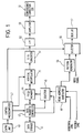
- FIGURE 1 is a block diagram showing a first embodiment of a digital convergence apparatus according to the present invention.
- the same elements as those shown in FIGURE 12 are assigned with the same reference numerals.
- Horizontal and vertical sync signals separated from video signals are provided to a read address generator 46.
- the read address generator 46 having an arrangement the same as the section 46 defined by the broken line in FIGURE 13 generates correction data read addresses (X address, Y address) based on the horizontal and vertical sync signals, and then outputs them to a selector 45.
- An entry unit 49 provides data to a control microcomputer 42 according to the manipulation by an operator.
- the control microcomputer 42 controls a data transfer controller 43 and supplies convergence correction data to a data storage 41 and a field memory 44 via the data transfer controller 43.
- the correction data is stored as it is for the correction executing points of the first adjusting line and a differential data of the correction data between the correction executing points is stored for the correction executing points of the second and subsequent adjusting lines. Further, the correction data and the differential data of the correction executing points include convergence correction data in the horizontal and vertical directions. The correction executing points are those points on the odd field.
- the data transfer controller 43 controls the selecting operation of the selector 45 and provides a write address to the field memory 44 via the selector 45 or a read address from the read address generator 46 to the field memory 44 via the selector 45.
- the selector 45 gives the write address to the field memory 44 in the data transfer and the read address to the field memory 44 in the scanning period.
- the data transfer controller 43 reads out the correction data and the differential data stored in the data storage 41 and gives the write address to the field memory 44 via the selector 45 to store the correction data and the differential data in the address corresponding to the position on the screen.
- the correction data or the differential data read out of the field memory 44 is supplied to a vertical interpolator 71.
- the vertical interpolator 71 interpolates the correction data between the correction executing points in the vertical direction.
- the correction data is obtained for each of all the scanning lines.
- the output of the vertical interpolator 71 is given to a D/A converter 51.
- the D/A converter 51 converts the correction data into the analog correction signal and output to an LPF 52.
- the LPF 52 interpolates the analog correction signal in the horizontal direction by eliminating the harmonic component and outputs the signal to an amplifier 53.
- the amplifier 53 amplifies the correction signal and supplies to a convergence correction coil 32.
- the convergence correction coil 32 improves the convergence by controlling the deflection of the electron beam according to the correction signal.
- the output of the read address generator 46 is also supplied to a pattern generator 56.
- the pattern generator 56 generates a pattern signal to indicate the convergence convergence correction pattern and outputs the signal to the selector 55.
- the selector 55 is controlled by the control microcomputer 42 and selecting either a video signal or the convergence correction pattern signal, supplies it to a display 57.
- the display 57 displays the input signal while the deflection of the screen is controlled by the convergence correction coil 32.
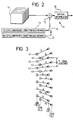
- FIGURE 2 is a block diagram showing the definite construction of the vertical interpolator 72 shown in FIGURE 1.
- the vertical interpolator 72 is comprised of a vertical interpolator 50, an adder 72, a first static convergence correction data memory 73, a second static convergence correction data memory 74 and a switch 75.
- the output of the field memory 44 is supplied to the adder 72.
- the adder 72 adds the static convergence correction data to the correction data read out of the field memory 44 and outputs to the vertical interpolator 50.
- the static convergence correction data the static convergence correction data S1 from the first static convergence correction data memory 73 and the static convergence correction data S2 from the second static convergence correction data memory 74 are selected and supplied to the adder 72.
- the first static convergence correction data memory 73 stores the static convergence correction data S1.
- the static convergence correction data S1 is for correcting the deviation of the static convergence generated by the effects of the earth magnetism due to the direction of installation, the secular change, etc.
- the second static convergence correction data memory 74 stores the static convergence correction data S2 which is obtained by further correcting the static convergence correction data S1 in response to the distance between the scanning lines in the odd and even fields. Further, as the static convergence correction data S2, for instance, an optimum data obtained while observing the convergence correction pattern in the actual convergence correction is set.
- These static convergence correction data S1 and S2 may be modified by the control microcomputer 42.
- the outputs of the first and the second static convergence correction data memories 73 and 74 are given to the adder 72 through the switch 75.
- the switch 75 selects the output of the first static convergence correction data memory 73 in the odd field and the output of the second static convergence correction data memory 74 in the even field and gives both outputs to the adder 72.
- the adder 72 adds the correction data with the static convergence correction data S1 or S2 and outputs to the vertical interpolator 50 and also, outputs the differential data as it is to the vertlcal interpolator 50.
- the vertical interpolator 50 is in the same construction as that of the broken lined portion 50 shown in FIGURE 13 and is comprised of a divider to divide the differential data by a divisor responsive to the number of scanning lines to be interpolated, an adder to accumulate the output of the divider, a register and a latch.
- the vertical interpolator 50 divides the differential data by a divisor which is according to the number of scanning lines to be interpolated and by accumulating the result of this division to the correction data with the static convergence correction data added, interpolates and outputs the correction data for each of all the scanning lines between the correction executing points.
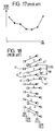
- FIGURE 3 shows the positions of the scanning lines before and after the convergence correction.
- the square marks represent the positions of the scanning lines in the odd and even fields before the correction, while the circles represent the positions of the scanning lines after the correction.
- the convergence correction is carried out before the shipment of the apparatus.
- the operator makes a convergence correction pattern to be displayed by manipulating the entry unit 49.
- the pattern signal from the pattern generator 56 is supplied to the display 57 via the selector 55 and for instance, a crosshatch pattern is displayed on the screen (not shown) of the display 57.
- the operator performs the convergence correction for each correction executing point by manipulating the entry unit 49 while observing the screen.
- the data from the entry unit 49 is given to the control microcomputer 42.
- the control microcomputer 42 gives the data corresponding to the correction executing point of the first adjusting line at the upper end of the screen directly to the data storage 41 and the field memory 44 as the correction data and gives the differential data with the correction data of the correction executing point of the preceding adjusting line to the data storage 41 and the field memory 44.
- This convergence correction corrects the deviation of the static convergence resulting from errors in the electron gun assembling, etc.
- the correction data is obtained for each of all the scanning lines using the correction data and the differential data stored in the data storage 41 and the static convergence correction data considering the effects of the place of installation and secular change.
- the data transfer controller 43 is controlled by the control microcomputer 42 and transfers the correction data and the differential data to the field memory 44.
- the read address generator 46 gives the read address (X address. Y address) to the field memory 44 via the selector 45. In this case, the read address is generated at the horizontal cycle and the same Y address continues by the number of times responsive to the number of scanning lines between the correction executing points in the vertical direction.
- the correction data from the field memory 44 is supplied to the vertical interpolator 71.
- the correction data is added with the static convergence correction data by the adder 72 of the vertical interpolator 71.
- +(12 - S1) is stored in the field memory 44 as the correction data in the vertical direction of the correction executing point K1 at the prescribed horizontal position of the prescribed adjusting line.
- the "+" sign of the correction data represents a convergence correction data in the upward direction, while the "-" sign represents a convergence correction data in the downward direction.
- FIGURE 3 shows the status of the correction of the scanning lines in the odd and even fields between the correction executing points K1 and K2.
- the correction data +(12 - S1) in the vertical direction for the correction executing point K1 which is read out of the field memory 44 is supplied to the adder 72.
- the switch 75 select the first static convergence correction data memory 73.
- the static convergence correction data S1 stored in the static convergence correction data memory 73 is supplied to the adder 72.
- the adder 72 adds the static convergence correction data S1 to the correction data and outputs +12 via the vertical interpolator 50.
- the output of the vertical interpolator 50 is converted into analog signal by the D/A converter 51, subject to the restriction of the band by the LPF 52 and after amplified by the amplifier 53, supplied to the convergence correction coil 32.
- the scanning line k1 of the correction executing point K1 in the odd field moves upward by the amount of movement corresponding to the correction data +12 according to the correction signal supplied to the vertical convergence correction coil of the convergence correction coil 32 as shown in FIGURE 3.
- the differential data -2n is read out of the field memory 44 at the timing when the scanning line k2 next to the scanning line k1 of the correction executing point K1 is input.
- the vertical interpolator 71 gives the differential data -2n as it is to the vertical interpolator 50.
- the vertical interpolator 50 multiplies the differential data by 2/n and adds it to the correction data of the scanning line of the correction executing point K1.
- This correction data is supplied to the convergence correction coil 32 through the D/A converter 51, the LPF 52 and the amplifier 53.
- the scanning line m1 which is next to the scanning line k1 of the correction executing point K1 is corrected.
- the correction data of the correction executing point K1 is also used.
- the correction data +(12 - S1) from the field memory 44 is supplied to the adder 72 of the vertical interpolator 72.
- the switch 75 selects the output of the second static convergence correction data memory 74 in the even field.
- the static convergence correction data S2 is supplied to the adder 72.
- a numerical data (S1 - 2) corresponding to the data "2" which represents the scanning line distance is set as the static convergence correction data S2.
- This correction data is supplied to the convergence correction coil 32 from the vertical interpolator 71 through the D/A converter 51, the LPF 52 and the amplifier 53.
- the scanning line m1 is corrected in the upward direction by the amount of movement corresponding to the correction data +10 as shown in FIGURE 3.
- the correction data is obtained using the differential data -2n between the correction executing points K1 and K2.
- the convergence is corrected according to this correction data and the scanning line m2 moves in the upward direction by 6 as shown in FIGURE 3. Thereafter, in the same manner as above, the correction data is obtained for each of all the scanning lines in the even field between the correction executing points K1 and K2 and the convergence is corrected.
- FIGURE 4 is a block diagram showing a second embodiment of the present invention, presenting the definite construction of the vertical interpolator.
- the same elements as those shown in FIGURE 2 are assigned with the same reference numerals and the explanations are omitted.
- the vertical interpolator 83 is comprised of a static convergence correction data output unit 80, a first offset data memory 81, a second offset data memory 82, the switch 75, the adder 72 and the vertical interpolator 50.
- the static convergence correction data output unit 80 stores the static convergence correction data S for correcting the deviation of the static convergence generated by the effects of the earth magnetism against the installing direction, secular change, etc. after the shipment of the projection type television receivers and the like.
- This static convergence correction data S is supplied to the adder 72.
- the output of the first or the second offset data memory 81 or 82 is given to the adder 72 through the switch 75.
- An offset data in the vertical direction for preventing the density of the scanning lines from lacking uniformity in the odd and even fields after the convergence correction is very small. Therefore, the correction data for the odd and even fields are corrected by adding an offset data to the static convergence correction data S in this embodiment.
- the first offset data memory 81 is a type of register for storing a first offset data for correcting the correction data in the odd field
- the second offset data memory 82 is also a type of register for storing a second offset data for correcting the correction data in the even field.
- the switch 75 gives the first offset data to the adder 72 in the odd field period, while the second offset data to the adder 72 in the even field period.
- the adder 72 adds the first or the second offset data to the correction data from the field memory 44, thereby preventing the density of the scanning lines from lacking uniformity resulting from offset of the positions of the scanning lines of the odd and even fields.
- the correction data is comprised of 12 bits more than 8 bits adopted for general video signals.
- the static convergence correction data is variable in 256 kinds which are expressed in 8 bits. In this embodiment, therefore, for instance, 8 bits in the most significant bit (MSB) side of the static convergence correction data S are given to the adder 72 and, for instance, 4 bits in the least significant bit (LSB) side of the first or the second offset data is given to the adder 72.
- MSB most significant bit
- LSB least significant bit
- the switch 75 selects the output of the first offset data memory 81.
- the adder 72 adds the 8 bits of the MSB side of the static convergence correction data with the 4 bits of the LSB side of the first offset data from the switch 75.
- the switch 75 selects the output of the second offset data memory 82 and gives to the adder 72.
- This embodiment has an advantage that the memory capacity can be reduced to less than that of the embodiment shown in FIGURE 2 as it is sufficient enough to provide one memory for storing the static convergence correction data and two memories for storing the offset data.
- FIGURE 5 is a block diagram showing a third embodiment of the present invention, presenting the definite construction of the vertical interpolator.
- the same elements as those shown in FIGURE 4 will be assigned with the same reference numerals and the explanations will be omitted.
- the vertical interpolator 85 of this embodiment is different from the vertical interpolator of the embodiment shown in FIGURE 4 in that the adders 47 and 84 are provided instead of the adder 72.
- the adder 47 adds the static convergence correction data S from the static convergence correction data output unit 80 to the correction data from the field memory 44 and outputs the added result to the adder 84.
- the adder 84 adds the first or the second offset data from the switch 75 to the output of the adder 47 and outputs the added result to the vertical interpolator 50.
- the static convergence correction data S is added to the correction data in the adder 47. Further, in the odd field the first offset data is added to the output of the adder 47 by the adder 84, while in the even field the second offset data is added to the output of the adder 47.
- FIGURE 6 is a block diagram showing a fourth embodiment of the present invention, presenting the definite construction of the vertical interpolator.
- the same elements as those shown in FIGURE 4 are assigned with the same reference numerals and the explanations are omitted.
- the vertical interpolator 98 of this embodiment is different from that of the embodiment shown in FIGURE 4 in that a first and a second offset data memories 96 and 97 are used for the first and the second offset data memories 81 and 82.
- the static convergence correction data are corrected for each field in response to the distance between the scanning lines, while the same correction data are used uniformly on the screen.
- optimum data corresponding to the positions on the screen are used as the correction data.
- first and the second offset data memories 96 and 97 optimum offset data corresponding to the odd and even field positions on the screen are stored. That is, the first and the second offset data memories 96 and 97 are the field memories to store offset data of the various points on the screen.
- the adder 72 when the correction data for the correction executing points of the first adjusting line are read out of the field memory 44 in the odd field, the adder 72 adds up the MSB of the static convergence correction data S and the LSB of the offset data from the first offset data memory 96. In this case, an optimum offset data is added according to the location on the screen. Thus, the convergence of the screen of the odd field is corrected with the high precision.
- the adder 72 adds up the MSB of the static convergence correction data S with the LSB of the offset data from the second offset data memory 97.
- the convergence of the screen of the even field is corrected with the high precision.
- FIGURE 7 is a block diagram showing a fifth embodiment of the present invention, presenting the definite construction of the vertical interpolator.
- the same elements as those shown in FIGURE 5 are assigned with the same reference numerals and the explanations are omitted.
- This embodiment enables the correction of the convergence of the HDTV (High Definition Television) system or the ATV (Advanced Television) system using the circuits adopted for the NTSC color television system.
- the vertical interpolator 90 of this embodiment is different from that of the embodiment shown in FIGURE 5 in that a switch 91 is used for the switch 75 and a first through a fourth offset data memories 92 through 95 are provided for the first and the second offset data memories 81 and 82.
- a switch 91 outputs the outputs of the first through the fourth offset data memories 92 through 95 selectively to the adder 84.
- the first and the second offset data memories 92 and 93 are the registers to maintain the first and the second offset data for correcting the correction data in the odd field and the third and the fourth offset data memories 94 and 95 are the registers to maintain the third and the fourth offset data for correcting the correction data in the even field.
- the switch 91 outputs the output of the first offset data memory 92 in the odd field and the output of the third offset data memory 93 in the even field.
- the switch 91 outputs the outputs of the first and the second offset data memories 92 and 93 by changing over them for every horizontal scanning period in the odd field and the outputs of the third and the fourth offset data memories 94 and 95 by changing over them for every horizontal scanning period in the even field.
- the first through the fourth offset data from the first through the fourth offset data memories are selectively supplies to the adder 84.
- the switch 91 outputs the output of the first offset data memory 92 in the odd field and the output of the third offset data memory 94 in the even field. In this case, the same operations as in the embodiment shown in FIGURE 4 are carried out.
- the switch 91 selects the outputs of the first and the second offset data memories 92 and 93 in the odd field. That is, the output of the first offset data memory 92 is selected in the odd line of the odd field and the output of the second offset data memory 93 is selected in the even line.
- the switch 91 selects the outputs of the first and the second offset data memories 92 and 93 in the odd field. That is, the output of the first offset data memory 92 is selected in the odd line of the odd field and the output of the second offset data memory 93 is selected in the even line.
- the switch 91 selects the output of the third offset data memory 94 in the odd line and the output of the fourth offset data memory 95 in the even line.
- the switch 91 is enabled to correct the convergence using the NTSC circuits also for the HDTV or the ATV circuits.
- the present invention can provide an extremely preferable digital convergence apparatus which improves the quality of screen by preventing the density of the scanning lines from lacking uniformity even when the convergence is corrected.
Landscapes
- Engineering & Computer Science (AREA)
- Multimedia (AREA)
- Signal Processing (AREA)
- Video Image Reproduction Devices For Color Tv Systems (AREA)
Applications Claiming Priority (2)
| Application Number | Priority Date | Filing Date | Title |
|---|---|---|---|
| JP6140504A JPH089405A (ja) | 1994-06-22 | 1994-06-22 | ディジタルコンバーゼンス装置 |
| JP140504/94 | 1994-06-22 |
Publications (2)
| Publication Number | Publication Date |
|---|---|
| EP0689363A2 true EP0689363A2 (de) | 1995-12-27 |
| EP0689363A3 EP0689363A3 (de) | 1997-05-28 |
Family
ID=15270187
Family Applications (1)
| Application Number | Title | Priority Date | Filing Date |
|---|---|---|---|
| EP95304367A Withdrawn EP0689363A3 (de) | 1994-06-22 | 1995-06-22 | Digitale Konvergenzvorrichtung |
Country Status (5)
| Country | Link |
|---|---|
| US (1) | US5592240A (de) |
| EP (1) | EP0689363A3 (de) |
| JP (1) | JPH089405A (de) |
| KR (1) | KR0167017B1 (de) |
| CA (1) | CA2152457A1 (de) |
Cited By (3)
| Publication number | Priority date | Publication date | Assignee | Title |
|---|---|---|---|---|
| DE19632188A1 (de) * | 1996-08-09 | 1998-02-12 | Thomson Brandt Gmbh | Verfahren und Vorrichtung zur Gewinnung von Korrekturwerten für Videozeilen eines Videobildes |
| WO2001041454A1 (en) * | 1999-11-30 | 2001-06-07 | Thomson Licensing S.A. | Projection television set with parity error checking |
| US6982766B1 (en) * | 1997-08-29 | 2006-01-03 | Thomson Licensing | Digital raster correction |
Families Citing this family (24)
| Publication number | Priority date | Publication date | Assignee | Title |
|---|---|---|---|---|
| JP3488314B2 (ja) * | 1995-04-21 | 2004-01-19 | ソニー株式会社 | 映像信号処理装置及び画像調整方法 |
| JPH0984035A (ja) * | 1995-09-08 | 1997-03-28 | Toshiba Corp | ディジタルコンバーゼンス装置 |
| KR0179844B1 (ko) * | 1995-10-06 | 1999-05-01 | 문정환 | 티브이의 화면 모서리 부분의 밝기 조정회로 |
| KR100200095B1 (ko) * | 1995-12-30 | 1999-06-15 | 윤종용 | 디지탈 컨버젼스를 이용한 화면 이펙트 방법 및회로 |
| US6014168A (en) * | 1996-04-26 | 2000-01-11 | Display Laboratories, Inc. | Screen mapping of a cathode ray tube |
| JPH11514813A (ja) * | 1996-04-26 | 1999-12-14 | フィリップス エレクトロニクス ネムローゼ フェンノートシャップ | スポット位置表示信号発生 |
| US6437829B1 (en) | 1997-01-16 | 2002-08-20 | Display Laboratories, Inc. | Alignment of cathode ray tube displays using a video graphics controller |
| US5969486A (en) * | 1997-01-16 | 1999-10-19 | Display Laboratories, Inc. | Detecting horizontal blanking time in cathode ray tube devices |
| US6285397B1 (en) | 1997-01-16 | 2001-09-04 | Display Laboratories, Inc. | Alignment of cathode ray tube video displays using a host computer processor |
| JP3634575B2 (ja) * | 1997-07-14 | 2005-03-30 | エヌイーシー三菱電機ビジュアルシステムズ株式会社 | デジタル画像補正装置及びディスプレイ装置 |
| KR100267729B1 (ko) * | 1998-04-30 | 2000-10-16 | 윤종용 | 영상 신호의 수평 편향 보간 장치 |
| US6753856B1 (en) * | 1998-05-12 | 2004-06-22 | Apple Computer, Inc. | System and method for dynamic correction of display characteristics |
| JP3395832B2 (ja) * | 1998-08-28 | 2003-04-14 | ソニー株式会社 | 画像表示補正システム、画像表示補正装置および方法並びに画像表示装置および方法 |
| US6486926B1 (en) * | 1999-09-29 | 2002-11-26 | Thomson Licensing S.A. | Adaptable raster distortion correction system for multiple horizontal scanning frequencies |
| US6292235B1 (en) * | 1999-09-29 | 2001-09-18 | Thomson Licensing S.A. | Distortion correction system with switchable digital filter |
| NO20000656A (no) * | 2000-02-09 | 2001-07-09 | Knut Krogstad | Digital korreksjonsmodul for videoprojektor |
| FR2810488B1 (fr) * | 2000-06-16 | 2002-08-30 | St Microelectronics Sa | Correction de convergence d'un ecran ou projecteur a tube cathodique |
| AU2003261448A1 (en) * | 2002-08-09 | 2004-02-25 | Iljin Diamond Co., Ltd. | Anti-contouring display correction |
| US7990840B2 (en) * | 2005-03-08 | 2011-08-02 | Qualcomm Incorporated | Methods and apparatus for efficient digital broadcast signaling in a wireless communications system |
| US7408595B2 (en) * | 2005-08-04 | 2008-08-05 | Tte Technology, Inc. | Method and apparatus for image correction |
| US7805260B2 (en) * | 2005-11-23 | 2010-09-28 | Electric Mirror, Llc | Mirror assembly |
| US8099247B2 (en) * | 2005-11-23 | 2012-01-17 | Electric Mirror, Llc | Back lit mirror with media display device |
| US7853414B2 (en) | 2005-11-23 | 2010-12-14 | Electric Mirror, Llc | Mounting structure for a mirror assembly |
| KR101339127B1 (ko) * | 2011-12-08 | 2013-12-09 | 아진산업(주) | 출력 지연으로 인한 노이즈를 제거할 수 있는 차량 어라운드 뷰 영상 생성방법 |
Family Cites Families (10)
| Publication number | Priority date | Publication date | Assignee | Title |
|---|---|---|---|---|
| JPS58101586A (ja) * | 1981-12-14 | 1983-06-16 | Sony Corp | コンバ−ゼンス補正回路 |
| JPS6178294A (ja) * | 1984-09-25 | 1986-04-21 | Sony Corp | デイジタルコンバ−ジエンス補正装置 |
| JP2634160B2 (ja) * | 1986-08-11 | 1997-07-23 | 日本放送協会 | 画像歪の補正方法 |
| JP2714023B2 (ja) * | 1988-01-29 | 1998-02-16 | 株式会社日立製作所 | 画像表示装置 |
| JP2637221B2 (ja) * | 1989-02-16 | 1997-08-06 | 株式会社日立製作所 | ディジタルコンバーゼンス補正装置 |
| DE69025526T2 (de) * | 1989-09-28 | 1996-09-19 | Matsushita Electric Ind Co Ltd | Digitale Konvergenzvorrichtung |
| DE3933950A1 (de) * | 1989-10-11 | 1991-04-18 | Thomson Brandt Gmbh | Einrichtung zur rasterkorrektur in einem fernsehgeraet |
| JP3029439B2 (ja) * | 1990-04-09 | 2000-04-04 | 株式会社日立製作所 | ディジタルコンバーゼンス補正データ作成方法 |
| JPH04207384A (ja) * | 1990-11-30 | 1992-07-29 | Hitachi Ltd | ディジタルコンバーゼンス補正装置 |
| JPH06141351A (ja) * | 1992-10-26 | 1994-05-20 | Matsushita Electric Ind Co Ltd | 信号発生装置 |
-
1994
- 1994-06-22 JP JP6140504A patent/JPH089405A/ja active Pending
-
1995
- 1995-06-22 CA CA002152457A patent/CA2152457A1/en not_active Abandoned
- 1995-06-22 EP EP95304367A patent/EP0689363A3/de not_active Withdrawn
- 1995-06-22 US US08/493,749 patent/US5592240A/en not_active Expired - Fee Related
- 1995-06-22 KR KR1019950016822A patent/KR0167017B1/ko not_active Expired - Fee Related
Non-Patent Citations (1)
| Title |
|---|
| None |
Cited By (4)
| Publication number | Priority date | Publication date | Assignee | Title |
|---|---|---|---|---|
| DE19632188A1 (de) * | 1996-08-09 | 1998-02-12 | Thomson Brandt Gmbh | Verfahren und Vorrichtung zur Gewinnung von Korrekturwerten für Videozeilen eines Videobildes |
| US6108054A (en) * | 1996-08-09 | 2000-08-22 | Deutsche Thomson Brandt Gmbh | Method and apparatus for obtaining correction values for video lines of a video frame |
| US6982766B1 (en) * | 1997-08-29 | 2006-01-03 | Thomson Licensing | Digital raster correction |
| WO2001041454A1 (en) * | 1999-11-30 | 2001-06-07 | Thomson Licensing S.A. | Projection television set with parity error checking |
Also Published As
| Publication number | Publication date |
|---|---|
| CA2152457A1 (en) | 1995-12-23 |
| US5592240A (en) | 1997-01-07 |
| JPH089405A (ja) | 1996-01-12 |
| EP0689363A3 (de) | 1997-05-28 |
| KR960003450A (ko) | 1996-01-26 |
| KR0167017B1 (ko) | 1999-03-20 |
Similar Documents
| Publication | Publication Date | Title |
|---|---|---|
| US5592240A (en) | Digital convergence apparatus | |
| CA2039143C (en) | Convergence control system for multiple vertical formats | |
| HK1004589B (en) | Convergence control system for multiple vertical formats | |
| EP0982934A2 (de) | Vorrichtung und Verfahren zur Korrektur der Ablenkverzerrung bei Kathodenstrahlröhren | |
| JPH05176238A (ja) | 撮像装置 | |
| US4549117A (en) | Circuit for generating signal for correcting deflection of electron beam | |
| JPH06141351A (ja) | 信号発生装置 | |
| US5793447A (en) | Digital convergence apparatus | |
| US5161002A (en) | Convergence control system for multiple vertical formats | |
| US6437522B1 (en) | Method for controlling digital dynamic convergence and system thereof | |
| US5301021A (en) | Display with vertical scanning format transformation | |
| EP0835583B1 (de) | Erzeugung von spline-wellenformen | |
| EP0774871A2 (de) | Projektor mit Schaltungsanordnung zum Korrigieren von Farbphasen- und Helligkeitsfehlern | |
| JPH045314B2 (de) | ||
| US20030098930A1 (en) | Digital dynamic convergence control system in a display system | |
| JPS6359191A (ja) | デイジタルコンバ−ゼンス装置 | |
| JP3352468B2 (ja) | コンバーゼンス自動調整装置 | |
| JPS631792B2 (de) | ||
| EP1013077B1 (de) | Digitale rasterkorrektur | |
| US6982766B1 (en) | Digital raster correction | |
| JPH0126234B2 (de) | ||
| US20050117076A1 (en) | Restration adjuser and registration adjusting method | |
| JP3402788B2 (ja) | ディジタルコンバーゼンス装置 | |
| JPH0750936B2 (ja) | デイジタルコンバ−ゼンス装置 | |
| JPS5842382A (ja) | デイジタルコンバ−ゼンス装置 |
Legal Events
| Date | Code | Title | Description |
|---|---|---|---|
| PUAI | Public reference made under article 153(3) epc to a published international application that has entered the european phase |
Free format text: ORIGINAL CODE: 0009012 |
|
| 17P | Request for examination filed |
Effective date: 19950713 |
|
| AK | Designated contracting states |
Kind code of ref document: A2 Designated state(s): DE FR GB NL |
|
| PUAL | Search report despatched |
Free format text: ORIGINAL CODE: 0009013 |
|
| AK | Designated contracting states |
Kind code of ref document: A3 Designated state(s): DE FR GB NL |
|
| 17Q | First examination report despatched |
Effective date: 19990519 |
|
| STAA | Information on the status of an ep patent application or granted ep patent |
Free format text: STATUS: THE APPLICATION IS DEEMED TO BE WITHDRAWN |
|
| 18D | Application deemed to be withdrawn |
Effective date: 19990921 |