EP0691741A2 - Verriegelungsschaltung - Google Patents
Verriegelungsschaltung Download PDFInfo
- Publication number
- EP0691741A2 EP0691741A2 EP95110429A EP95110429A EP0691741A2 EP 0691741 A2 EP0691741 A2 EP 0691741A2 EP 95110429 A EP95110429 A EP 95110429A EP 95110429 A EP95110429 A EP 95110429A EP 0691741 A2 EP0691741 A2 EP 0691741A2
- Authority
- EP
- European Patent Office
- Prior art keywords
- state
- switch means
- latch circuit
- input terminal
- switch
- Prior art date
- Legal status (The legal status is an assumption and is not a legal conclusion. Google has not performed a legal analysis and makes no representation as to the accuracy of the status listed.)
- Granted
Links
Images







Classifications
-
- H—ELECTRICITY
- H03—ELECTRONIC CIRCUITRY
- H03K—PULSE TECHNIQUE
- H03K3/00—Circuits for generating electric pulses; Monostable, bistable or multistable circuits
- H03K3/02—Generators characterised by the type of circuit or by the means used for producing pulses
- H03K3/027—Generators characterised by the type of circuit or by the means used for producing pulses by the use of logic circuits, with internal or external positive feedback
- H03K3/037—Bistable circuits
-
- H—ELECTRICITY
- H03—ELECTRONIC CIRCUITRY
- H03K—PULSE TECHNIQUE
- H03K3/00—Circuits for generating electric pulses; Monostable, bistable or multistable circuits
- H03K3/01—Details
- H03K3/012—Modifications of generator to improve response time or to decrease power consumption
Definitions
- This invention pertains to a latch circuit for use in semiconductor integrated circuits.
- a chopper inverter amplifier is often used in analog-to-digital (A/D) converters.
- a comparator is made up of a chopper inverter amplifier and a latch circuit that is located at a stage after the chopper inverter amplifier.
- This latch circuit includes two inverters (the first- and second-stage inverters) connected in series, an input switch connected between an input terminal of the first-stage inverter and an output terminal of the chopper inverter amplifier, and a feedback switch connected between the input terminal of the first-stage inverter and an output terminal of the second-stage inverter.
- FIGURE 22 illustrates a conventional latch circuit structure.
- 51 is an external input terminal.
- 52 is a first inverter.
- 53 is a second inverter.
- 54 is an external output terminal.
- An input switch S1 is made up of a PMOS 55a and an NMOS 55b .
- a feedback switch S2 is made up of a PMOS 56a and an NMOS 56b .
- a control voltage V ⁇ is applied to a gate of the PMOS 55a and to a gate of the NMOS 56b
- a control voltage /V ⁇ that is an inversion of the control voltage V ⁇ is applied to a gate of the NMOS 55b and to a gate of the PMOS 56a .
- V ⁇ is HIGH, then /V ⁇ is LOW. Both the PMOS 55a and the NMOS 55b go into the nonconducting state, and the input switch S1 turns off. Meanwhile, both the PMOS 56a and the NMOS 56b go into the conducting state, and the feedback switch S2 turns on. This period is called a feedback period. If V ⁇ is LOW, then /V ⁇ becomes HIGH. The PMOS 55a and the NMOS 55b each go into the conducting state, and the input switch S1 turns on. On the other hand, the PMOS 56a and the NMOS 56b each go into the nonconducting state, and the feedback switch S2 turns off. This period is called a sampling period. In the FIGURE 22 latch circuit, the input switch S1 and the feedback switch S2 make their transition at the same time.
- V in (the voltage applied at the external input terminal 51 ) is greater than V a (the first inverter's 52 threshold voltage) at the end of a sampling period, then an output voltage of the second inverter 53 is fed back in a positive feedback manner to become V DD (the supply voltage) in a feedback period. If V in is lower than V a at the end of a sampling period, then an output voltage of the second inverter 53 is fed back in a positive feedback manner to become V SS (the ground voltage) in a feedback period.
- a conventional latch circuit presents the following problems.
- the inventors of the present application found that in actual latch circuit operations a phenomenon that the input switch S1 and the feedback switch S2 simultaneously have an on state occurs resulting in impeding high-speed, high-accuracy latch circuit operations.
- FIGURE 23 shows the operation of the input switch S1 as well as the operation of the feedback switch S2 .
- V ⁇ remains HIGH until time t1, which is to say, the latch circuit is in a feedback period.
- V ⁇ begins making a HIGH ⁇ LOW transition at time t1 and the latch circuit holds V DD in a feedback period.
- Applied at terminals of the input switch S1 are V in applied at the external input terminal 51 and V DD held by the latch circuit. As shown in a graph (the above one) of FIGURE 23 , the PMOS 55a of the input switch S1 conducts when V ⁇ becomes lower than V DD by V tp (the threshold voltage), and the NMOS 55b of the input switch S1 conducts when /V ⁇ becomes greater than V in by V tn (the threshold voltage).
- V DD Applied at the terminals of the feedback switch S2 is V DD held by the latch circuit.
- the PMOS 56a of the feedback switch S2 goes into the nonconducting state when /V ⁇ becomes lower than V DD by V tp , and the NMOS 56b of the feedback switch S2 remains nonconducting because it is impossible for V ⁇ to become greater than V DD by V tn .
- FIGURE 24 The operation of the latch circuit is shown in FIGURE 24 .
- the FIGURE 24 latch circuit has the first inverter 52 , the second inverter 53 , and the input switch S1 , and the feedback switch S2 .
- 61 is a preceding-stage amplifier.
- FIGURE 24 there exists a first transitional period during which both the input switch S1 and the feedback switch S2 have an on state at the same time when there is made a feedback ⁇ sampling transition, while there exists a second transitional period during which both the input switch S1 and the feedback switch S2 have an on state at the same time when there is made a sampling ⁇ feedback transition.
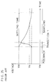
- FIGURE 25 is a graph showing changes in the output voltage of the amplifier 61 in the first transitional period.
- the amplifier's 61 output voltage is represented by solid line and the second inverter's 53 output voltage is represented by dot-dash line.
- V a is the first inverter's 52 threshold voltage.
- the second inverter's 53 output voltage is V DD .
- the amplifier 61 outputs a voltage of V in that is slightly lower than V a .
- both the input switch S1 and the feedback switch S2 each have an on state, as a result of which the amplifier's 61 output voltage is driven to the second inverter 53 to go up to near V DD .
- the feedback switch S2 turns off, so that the amplifier's 61 output voltage is again driven to V in .
- the amplifier's 61 output voltage has been increased to near V DD in the first transitional period, so that it needs a period of time known as the settling time to become V in again.
- the latch circuit is likely to hold V DD although V in was lower than V a . This prolongs the length of the sampling period because the settling time must be included therein. More specifically, 10-15 ns is required, thereby producing a bar to high-speed latch circuit operations.
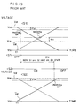
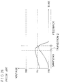
- FIGURE 26 is a graph showing changes in the input voltage of the first inverter 52 in the second transitional period.
- the first inverter's 52 input voltage is represented by solid line and the second inverter's 53 output voltage is represented by dot-dash line.
- V a is the first inverter's 52 threshold voltage.
- the second inverter's 53 output voltage changes with a delay with respect to the first inverter's 52 input voltage. If the latch circuit goes into the second transitional period when the first inverter's 52 input voltage exceeds V a and when the second inverter's 53 output voltage is below V a , both the input switch S1 and the feedback switch S2 have an on state and the first inverter's 52 input voltage is driven to the second inverter 53 to become lower than V a .
- the latch circuit comes to hold V SS in the feedback period although the first inverter's 52 input voltage was higher than V a at the end of the sampling period. The accuracy of latch circuit operation is reduced.
- an object of the present invention is to provide an improved latch circuit capable of high-speed, high-accuracy operations by preventing the input switch and the feedback switch from having at the same time an on state.
- the present invention provides a latch circuit comprising: an external input terminal for accepting a voltage coming in from outside the latch circuit; a noninverting amplifier with an input terminal and an output terminal for amplifying the voltage in a noninverting amplification manner; a first switch means which is connected between the external input terminal and the input terminal of the noninverting amplifier and which is capable of having either an on state for establishing a connection between the external input terminal and the input terminal of the noninverting amplifier or an off state for establishing a disconnection between the external input terminal and the input terminal of the noninverting amplifier; a second switch means which is connected between the input terminal and the output terminal of the noninverting amplifier and which is capable of having either an on state for establishing a connection between the input and output terminals of the noninverting amplifier or an off state for establishing a disconnection between the input and output terminals of the noninverting amplifier; a control means for controlling the on/off state of the first switch means and the on/off state of the second switch means in such
- this latch circuit it is arranged such that the first and second switch means do not have at the same time an on state. This eliminates a period for the noninverting amplifier to drive a voltage coming in from the external input terminal. Input voltage disturbance occurring in a conventional latch circuit can be controlled thereby improving the rate and accuracy of latch circuit operation.
- control means may include: a first drive means for driving the first switch means for setting the state thereof; a second drive means for driving the second switch means for setting the state thereof; a delay means for receiving a first signal and delaying same to generate a second signal; a signal generation means which receives the first signal and the second signal, to generate a third signal prompting the first switch means to change state, the generated third signal being forwarded to the first drive means, and to generate a fourth signal prompting the second switch means to change state, the generated fourth signal being forwarded to the second drive means.
- the noninverting amplifier may comprise an even number of inverting amplifiers connected in series.
- the latch circuit may include a capacitor with two terminals, one of which being connected to an input terminal of a first-stage inverting amplifier of the inverting amplifiers and the other of which being connected to an output terminal of the first-stage inverting amplifier.
- the provision of the capacitor reduces the effect of a parasitic capacitor. This reduces not only the error voltage in the input voltage of the latch circuit but also the error voltage variation due to the semiconductor integrated circuit fabrication process.
- the latch circuit may include a capacitor with two terminals, one of which being connected to an input terminal of a last-stage inverting amplifier of the inverting amplifiers and the other of which being connected to an output terminal of the last-stage inverting amplifier.
- the provision of the capacitor reduces the effect of the operation of a circuit located at a stage after the latch circuit, and voltage transition disturbance in a latch circuit feedback operation can be controlled.
- the latch circuit may include a capacitor with two terminals, one of which being connected to an input terminal of the noninverting amplifier and the other of which being connected to an output terminal of the noninverting amplifier.
- the provision of the capacitor reduces the effect of a parasitic capacitor. This reduces not only the error voltage in the input voltage of the latch circuit but also the error voltage variation due to the semiconductor integrated circuit fabrication process.
- the present invention provides a latch circuit comprising: an external input terminal for accepting a voltage coming in from outside the latch circuit; a noninverting amplifier with an input terminal and an output terminal, consisting of N inverting amplifiers connected in series, where the number N is even, for amplifying the voltage in a noninverting amplification manner; a first switch means which is connected between the external input terminal and the input terminal of the noninverting amplifier and which is capable of having either an on state for establishing a connection between the external input terminal and the input terminal of the noninverting amplifier or an off state for establishing a disconnection between the external input terminal and the input terminal of the noninverting amplifier; a second switch means which is connected between the input terminal and the output terminal of the noninverting amplifier and which is capable of having either an on state for establishing a connection between the input and output terminals of the noninverting amplifier or an off state for establishing a disconnection between the input and output terminals of the noninverting amplifier; N bias switch means each of which is connected
- the above-described latch circuit may include a control means for controlling the on/off state of the first switch means and the on/off state of the second switch means in such a way as to prevent both the first switch means and the second switch means from having an on state at the same time when the first switch means and the second switch means together make their respective state transitions.
- a voltage, held by the latch circuit in the feedback period changes to a threshold voltage, and the settling time taken for setting a voltage applied at the external input terminal to a final voltage in a sampling period is not affected by a difference in the voltage held by the latch circuit in the preceding feedback period.
- the noninverting amplifier may include (N - 1) capacitors connected in series between an output terminal of an ith-stage inverting amplifier of the N inverting amplifiers and an input terminal of an (i + 1)th-stage inverting amplifier of the N inverting amplifiers, where the number i is an integer satisfying a condition of 1 ⁇ i ⁇ (N - 1) .
- This capacitor is able to hold a difference between a threshold voltage of an inverting amplifier and that of an adjoining inverting amplifier. This reduces the inverting amplifier threshold voltage variation thereby improving the accuracy of latch circuit operation.
- FIGURE 1 is a block diagram outlining a structure of a first latch circuit in accordance with the present invention.
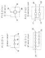
- FIGURE 2 comprised of FIGURES 2a , 2b , 2c , and 2d , shows structural elements of the first latch circuit of FIGURE 1 , wherein FIGURE 2a shows a delay circuit, and FIGURE 2b shows a switch device, and FIGURE 2c shows a drive circuit, and FIGURE 2d shows a composite gate.
- FIGURE 3 is a circuit diagram showing an embodiment of the first latch circuit.
- FIGURE 4 is an input/output signal timing diagram for a composite gate included in the first latch circuit.
- FIGURE 5 is a timing diagram useful in understanding the operation of a latch section of the first latch circuit.
- FIGURE 6 is a graph showing changes in the voltage applied at an external input terminal, in the operation of the latch section of the first latch circuit.
- FIGURE 7 illustrates an embodiment of a second latch circuit in accordance with the present invention.
- FIGURE 8 is an input/output signal timing diagram for a composite gate included in the second latch circuit.
- FIGURE 9 is a timing diagram useful in understanding the operation of a latch section of the second latch circuit.
- FIGURE 10 is a graph showing changes in the voltage applied at an external input terminal, in the operation of the latch section of the second latch circuit.
- FIGURE 11 comprised of FIGURES 11a and 11b , shows structural elements of a third latch circuit in accordance with the present invention, wherein FIGURE 11a shows a composite gate and FIGURE 11b shows a delay circuit.
- FIGURE 12 shows an embodiment of the third latch circuit.
- FIGURE 13 is an input/output signal timing diagram for a composite gate included in the second latch circuit.
- FIGURE 14 is a timing diagram useful in understanding the operation of a latch section of the third latch circuit.
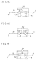
- FIGURE 15 illustrates a latch section of a fourth latch circuit in accordance with the present invention.
- FIGURE 16 illustrates a latch section of a fifth latch circuit in accordance with the present invention.
- FIGURE 17 illustrates a latch section of a sixth latch circuit in accordance with the present invention.
- FIGURE 18 illustrates a latch section of a seventh latch circuit in accordance with the present invention.
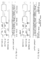
- FIGURE 19 comprised of FIGURES 19a and 19b , wherein FIGURE 19a is a timing diagram useful in understanding the operation of a latch section of the seventh latch circuit and FIGURE 19b is a timing diagram useful in understanding the operation of the seventh latch circuit employed as a latch section in the first latch circuit.
- FIGURE 20 is a circuit diagram showing an eighth latch circuit in accordance with the present invention.
- FIGURE 21 is a timing diagram useful in understanding the operation of the eighth latch circuit.
- FIGURE 22 is a circuit diagram showing a conventional latch circuit structure.
- FIGURE 23 shows the operation of an input switch as well as the operation of a feedback switch in a conventional latch circuit.
- FIGURE 24 is a diagram showing the operation of a conventional latch circuit.
- FIGURE 25 is a graph showing changes in the output voltage of an amplifier 61 in the operation of a conventional latch circuit.
- FIGURE 26 is a graph showing changes in the input voltage of a first inverter 52 in the operation of a conventional latch circuit.
- a latch circuit in accordance with the present invention comprises an inverter, a switch, a logical circuit, a delay circuit, and the like.
- An inverter is formed by a circuit which takes in a positive voltage and puts out a negative one, or vice versa such as a CMOS inverter, an E/D inverter, and an NMOS inverter.
- a switch is formed by a CMOS switch, an NMOS switch, or a PMOS switch.
- FIGURE 1 outlines a first latch circuit of the present invention.
- the first latch circuit has a latch section 12 formed by an external input terminal 1 , a first inverter 2 , a second inverter 3 , an external output terminal 4 , an input switch S1 as a first switch means, and a feedback switch S2 as a second switch means.
- the first and second inverters 2 and 3 together form a noninverting amplifier 5 .
- the input switch S1 is connected between the external input terminal 1 and an input terminal of the first inverter 2 . When the input switch S1 has an on state, an input voltage applied at the external input terminal 1 is fed to the first inverter 2 .
- the first inverter 2 is associated with the input switch S1 and acts as an amplifier for input voltage inverting amplification.
- the second inverter 3 is connected in series to the first inverter 2 and acts as an amplifier for inversion-amplifying an output voltage of the first inverter 2 .
- the feedback switch S2 is connected between the input terminal of the first inverter 2 and an output terminal of the second inverter 3 . When the feedback switch S2 has an on state, an output voltage of the second inverter 3 is fed back in a positive feedback manner to the first inverter 2 via the feedback switch S2 .
- the external output terminal 4 is an output terminal at which an output voltage of the second inverter 3 is put out to outside the latch circuit.
- the first latch circuit has a control section 11 comprising a first drive circuit 6 , a second drive circuit 7 , a composite gate 8 as a signal generation means, a delay circuit 9 , and a signal input terminal 10 .
- the first drive circuit 6 is operable to turn on or off the input switch S1
- the second drive circuit 7 is operable to turn on or off the feedback switch S2 .
- the composite gate 8 accepts a signal from the signal input terminal 10 and a signal from the delay circuit 9 and performs a logical operation on the signals received.
- the signal input terminal 10 is an input terminal for accepting a basic clock signal based on which each operation period of the latch section 12 is determined.
- FIGURE 2a is a circuit diagram depicting an example of the delay circuit 9 .
- the delay circuit 9 is made up of a first-stage inverter 14 and a second-stage inverter 15 connected together in series.
- a sum of the time taken for a pulse to traverse the inverter 14 and the time taken for a pulse to traverse the inverter 15 is the delay circuit's 9 delay time. Since the number of inverters to be connected in series is designed to be even, a signal taken in at an input terminal 13 and a signal put out at an output terminal 16 have the same polarity.
- FIGURE 2b is a circuit diagram showing an example of the switch S1 ( S2 ). Since the input switch S1 and the feedback switch S2 are identical in configuration with each other, only the input switch S1 is described here.
- the input switch S1 is a transmission gate formed by a PMOS transistor and an NMOS transistor.
- the input switch S1 has input terminals 17 , 18 and control terminals 19 , 20 .
- the FIGURE 2b switch is turned on or off by control signals applied at the control terminals 19 and 20 .
- FIGURE 2c is a circuit diagram showing an example of the drive circuit 6 ( 7 ). Since the drive circuits 6 and 7 are identical circuits, only the drive circuit 6 is described here. As shown in FIGURE 2c , the drive circuit 6 is formed by an in-series connection path consisting of five inverters connected in series and a branch path consisting of three inverters connected in series and branching off at the output side of a first-stage inverter of the in-series connection path.
- the drive circuit 6 has an input terminal 21 , an inverting output terminal 22 , and a noninverting output terminal 23 . If a signal, taken in at the input terminal 21 , is transmitted through the in-series connection path, an inverting signal is put out at the inverting output terminal 22 .
- FIGURE 2d is a circuit diagram showing an example of the composite gate 8 .
- this composite gate 8 is made up of a first NAND gate with two input terminals associated with a terminal I1 , a first inverter which is connected to a stage after the first NAND gate and which has an output terminal associated with a terminal O1 , a second NAND gate with two input terminals respectively associated with the terminal I1 and a terminal I2 , and a second inverter which is connected to a stage after the second NAND gate and which has an output terminal associated with a terminal O2 .
- FIGURE 3 is an embodiment of the first latch circuit. This embodiment is implemented employing the FIG. 2a delay circuit, the FIG. 2b switch, the FIG. 2c drive circuit, and the FIG. 2d composite gate.
- the terminal 17 of the input switch S1 is connected to the external input terminal 1 and the terminal 18 thereof is connected to the input terminal of the noninverting amplifier 5 .
- the terminal 17 of the feedback switch S2 is connected to the input terminal of the noninverting amplifier 5 and the terminal 18 thereof is connected to the output terminal of the noninverting amplifier 5 .
- the input terminal 13 of the delay circuit 9 is connected to the signal input terminal 10 .
- the terminal I1 of the composite gate 8 is connected to the signal input terminal 10 and the terminal I2 is connected to the output terminal 16 of the delay circuit 9 .
- the terminal O1 of the composite gate 8 is connected to the input terminal 21 of the second drive circuit 7 and the terminal O2 thereof is connected to the input terminal 21 of the first drive circuit 6 .
- the inverting output terminal 22 of the first drive circuit 6 is connected to the terminal 19 of the input switch S1 and the noninverting output terminal 23 thereof is connected to the terminal 20 of the input switch S1 .
- the inverting output terminal 22 of the second drive circuit 7 is connected to the terminal 20 of the feedback switch S2 and the noninverting output terminal 23 thereof is connected to the terminal 19 of the feedback switch S2 .
- the internal organization of each of the first drive circuit 6 , the second drive circuit 7 , and the composite gate 8 is not shown in FIGURE 3 .
- the operation of the first latch circuit is explained by making reference to FIGURES 4 and 5 .
- FIGURE 4 is an input/output signal timing diagram for the composite gate 8 .
- a basic clock signal is directly applied to the terminal I1 of the composite gate 8 from the signal input terminal 10 .
- This basic clock signal is also indirectly applied to the terminal I2 of the composite gate 8 via the delay circuit 9 .
- the terminal I2 accepts a delayed clock signal that is delayed by means of the delay circuit 9 a specific amount with respect to the basic clock signal.
- the composite gate 8 puts out at the terminal O1 a first signal identical in waveform with the basic clock signal.
- the composite gate 8 further puts out at the terminal O2 a second signal that is delayed only in the rising timing with respect to the first signal.
- the first drive circuit 6 generates from a signal from the terminal O2 of the composite gate 8 a noninverting signal and an inverting signal, for on-off controlling of the input switch S1 .
- the second drive circuit 7 generates from a signal from the terminal O1 of the composite gate 8 a noninverting signal and an inverting signal, for on-off controlling of the feedback switch S2 .
- FIGURE 5 is a timing diagram showing the operation of the latch section 12 .
- the latch section 12 is characterized in that there is established a separation period between a feedback period and a sampling period, during which both the input switch S1 and the feedback switch S2 have an off state.
- the input switch S1 has an on state while on the other hand the feedback switch S2 has an off state.
- the first inverter 2 takes in a voltage, applied at the external input terminal 1 , as its input voltage.
- the first inverter 2 inversion-amplifies this input voltage on the basis of V a (the threshold voltage).
- This inversion-amplified voltage is further inversion-amplified by the second inverter 3 and is put out.
- a voltage that the first inverter 2 takes in and a voltage that the second inverter 3 puts out have the same polarity on the basis of V a .
- the input switch S1 has an off state while the feedback switch S2 has an on state.
- the on/off state of the input switch S1 and the on/off state of the feedback switch S2 are switched simultaneously.
- an output voltage of the second inverter 3 is fed back, in a positive feedback manner, to the input terminal of the first inverter 2 by way of the feedback switch S2 that is now in the on state. Because of such positive feedback, an input voltage of the first inverter 2 and an output voltage of the second inverter 3 are driven to the supply voltage or ground voltage.
- V a i.e., the first inverter's 2 threshold voltage
- the input switch S1 stays off while the feedback switch S2 makes an on ⁇ off transition.
- a separation period Such a situation where both the input switch S1 and the feedback switch S2 have an off state is called a separation period.
- the provision of the separation period prevents the input switch S1 and the feedback switch S2 from simultaneously having an on state.
- a conventional latch circuit produces the phenomenon that in the feedback ⁇ sampling transition a voltage that the external input terminal 1 accepts is driven towards a voltage held by the second inverter 3 in the feedback period
- the present invention prevents the occurrence of such a phenomenon. Additionally this enables a circuit located at a preceding stage to the latch circuit to operate without distortion.
- FIGURE 6 is a graph showing changes in the voltage applied at the external input terminal 1 in a feedback ⁇ sampling transition.
- the voltage applied at the external input terminal 1 is represented by solid line and the voltage held by the second inverter 3 in the feedback period is represented by dot-dash line.
- a voltage applied at the external input terminal 1 is not affected by a voltage held by the second inverter 3 in the feedback period because there is provided a separation period. Since the settling time can be reduced, this provides fast latch operations. A separation period of, say, about 1.5 ns will produce sufficient effects. Therefore the separation period can be set much lower than the settling time (10-15 ns).
- the control section 11 consisting of the first drive circuit 6 , the second drive circuit 7 , the composite gate 8 , and the delay circuit 9 , controls in an active manner the operation order of the switches S1 and S2 of the latch section 12 , and a separation period is established between a feedback period and a sampling period.
- This arrangement not only allows a circuit located at a preceding stage to the latch circuit to operate without distortion but also enables high-speed latch operations.
- FIGURE 7 illustrates an embodiment of the second latch circuit.
- the second latch circuit is made up of different circuits as shown in FIGURE 2 . Only features of the second latch circuit are described here.
- the terminal I1 of the composite gate 8 is connected to the signal input terminal 10 while the terminal I2 thereof is connected to the output terminal 16 of the delay circuit 9 .
- the terminal I2 of the composite gate 8 is connected to the signal input terminal 10 while the terminal I1 thereof is connected to the output terminal 16 of the delay circuit 9 .
- the second latch circuit is identical in configuration with the first latch circuit. Elements in the second embodiment, which are functionally equivalent to their counterparts of the first embodiment, are thus assigned the same reference numerals and they are not described in detail here accordingly.
- FIGURE 8 is an input/output signal timing diagram for the composite gate 8 .
- a delayed clock signal that is delayed by the delay circuit 9 for a specific amount with respect to a basic clock signal is applied to the terminal I1 of the composite gate 8 .
- the terminal I2 of the composite gate 8 accepts a basic clock signal directly from the signal input terminal 10 .
- the composite gate 8 provides a first signal identical in waveform with the basic clock signal at the terminal O1 .
- the composite gate 8 further puts out a second signal that is advanced only in the falling timing with respect to the first signal, at the terminal O2 .
- the first drive circuit 6 generates from a signal from the terminal O2 of the composite gate 8 a noninverting signal and an inverting signal for on-off controlling of the input switch S1.
- the second drive circuit 7 generates from a signal from the terminal O1 of the composite gate 8 a noninverting signal and an inverting signal for on-off controlling of the feedback switch S2 .
- FIGURE 9 is a timing diagram showing the operation of the latch section 12 .
- the latch section 12 is characterized in that there is established a hold period between a sampling period and a feedback period, during which both the input switch S1 and the feedback switch S2 have an off state.
- the feedback switch S2 stays off while the input switch S1 makes an on ⁇ off transition.
- a hold period Such a situation where both the input switch S1 and the feedback switch S2 are in the off state is called a hold period.
- the provision of the hold period prevents the input switch S1 and the feedback switch S2 from simultaneously having an on state.
- a conventional latch circuit produces the phenomenon that in a sampling ⁇ feedback transition a voltage applied at the external input terminal 1 is driven towards a voltage provided by the second inverter 3 in a sampling period
- the present invention prevents the occurrence of such a phenomenon. Additionally this enables a circuit located at a preceding stage to the latch circuit to operate without distortion.
- FIGURE 10 is a graph showing changes in the input voltage of the first inverter 2 in a sampling ⁇ feedback transition.
- the input voltage of the first inverter 2 is represented by solid line and the output voltage of the second inverter 3 is represented by dot-dash line.
- an input voltage of the first inverter 2 is not affected by an output voltage of the second inverter 3 , being maintained at the same level as at the end of the sampling period. Since the first inverter 2 takes in a voltage greater than V a (i.e., the first inverter's 2 threshold voltage), this causes the second inverter 3 to provide a supply voltage in a feedback period. This provides improvements in latch circuit operation accuracy.
- the control section 11 consisting of the first drive circuit 6 , the second drive circuit 7 , the composite gate 8 , and the delay circuit 9 , controls in an active manner the operation order of the switches S1 and S2 of the latch section 12 , and a hold period is established between a sampling period and a feedback period.
- This arrangement not only enables a circuit located at a preceding stage to the latch circuit to operate without distortion but also improves the accuracy of latch circuit operation.
- FIGURE 11a shows an example of a composite gate 8A for use in the third latch circuit.
- the composite gate 8A is composed of a first NAND gate with two input terminals both connected to a terminal I1 , a first inverter which is connected to the next stage after the first NAND gate and which has an output terminal connected to a terminal O1 , a second NAND gate with two input terminals, one of which being connected to a terminal I2 and the other being connected to a terminal I3 , and a second inverter which is connected to the next stage after the second NAND gate and which has an output terminal connected to a terminal O2 .
- FIGURE 11b shows an example of a delay circuit 9A employed in the third latch circuit.
- the delay circuit 9A is composed of a first delay section circuit of inverters 25 and 26 connected in series and a second delay section circuit of inverters 27 and 28 connected in series, the first and second delay sections being connected together in series.
- a sum of the time taken for a pulse to traverse the inverter 25 and the time taken for a pulse to traverse the inverter 26 is defined as the first delay time
- a sum of the time taken for a pulse to traverse the inverter 27 and the time taken for a pulse to traverse the inverter 28 is defined as the second delay time. Since the number of inverters to be connected in series in each of the first and second delay section circuits is designed to be even, a signal applied at an input terminal 24 and signals provided at output terminals 29 and 30 are the same in polarity.
- FIGURE 12 shows an embodiment of the third latch circuit wherein FIGURE 2b switches are used as the input switch S1 and as the feedback switch S2 , FIGURE 2c drive circuits are used as the first drive circuit 6 and as the second drive circuit 7 , a FIGURE 11a composite gate is used as the composite gate 8A , and a FIGURE 11b delay circuit is used as the delay circuit 9A .
- the input terminal 24 of the delay circuit 9A is connected to the signal input terminal 10 .
- the terminal I1 of the composite gate 8A is connected to the output terminal 29 of the delay circuit 9A , and the terminal I2 is connected to the signal input terminal 10 , and the terminal I3 is connected to the output terminal 30 of the delay circuit 9A .
- the terminal O1 of the composite gate 8A is connected to the input terminal 21 of the second drive circuit 7 and the terminal O2 is connected to the input terminal 21 of the first drive circuit 6 .
- the second latch circuit is identical in organization with the first and second latch circuits.
- FIGURE 13 is an input/output signal timing diagram for the composite gate 8A .
- a basic clock signal is delayed by the first delay section circuit of the delay circuit 9A by the first delay time, thereafter being applied as a first delayed clock signal to the terminal I1 of the composite gate 8A .
- the terminal I2 of the composite gate 8A accepts a basic clock signal directly from the signal input terminal 10 .
- the first delayed clock signal is further delayed by the second delay section circuit of the delay circuit 9A by the second delay time, thereafter being applied as a second delayed clock signal to the terminal I3 of the composite gate 8A .
- the composite gate 8A operates to provide a first signal identical in waveform with the basic clock signal at the terminal O1 .
- the composite gate 8A further provides, at the terminal O2 , a second signal that is delayed in the rising timing and advanced in the falling timing with respect to the first signal.
- the first drive circuit 6 generates from a signal from the terminal O2 of the composite gate 8 a noninverting signal and an inverting signal for on-off controlling of the input switch S1 .
- the second drive circuit 7 generates from a signal from the terminal O1 of the composite gate 8 a noninverting signal and an inverting signal for on-off controlling of the feedback switch S2 .
- FIGURE 14 is a timing diagram showing the operation of the latch section 12 of the third latch circuit.
- the latch section 12 is characterized in that there is established not only a separation period between a feedback period and a sampling period during which both the input switch S1 and the feedback switch S2 have an off state but also a hold period between a sampling period and a feedback period during which both the input switch S1 and the feedback switch S2 have an off state.
- the latch section 12 of the third latch circuit operates in the same way that the first and second latch circuits operate and the operation of each period is not described here.
- the control section 11 consisting of the first drive circuit 6 , the second drive circuit 7 , the composite gate 8A , and the delay circuit 9A , controls in an active manner the operation order of the switches S1 and S2 of the latch section 12 , and a separation period between a feedback period and a sampling period as well as a hold period between a sampling period and a feedback period is provided.
- This arrangement not only enables a circuit located at a preceding stage to the latch circuit to operate without distortion but also increases the rate and accuracy of latch circuit operation.
- FIGURE 15 is a circuit diagram of a latch section of the fourth latch circuit.
- the latch section of the fourth latch circuit is identical in configuration with the latch section 12 of the first latch circuit of FIGURE 1 except that the present latch section has a capacitor C1 connected between the input and output terminals of the first inverter 2 .
- the capacitor C1 is provided to reduce the degree of affection produced by a parasitic capacitor Cs between the input terminal of the first inverter 2 and ground.
- the latch section of the fourth latch circuit may find applications in any one of the first, second, and third latch circuits. However, a case where the present latch section is used in the second latch circuit is described here because the effect of the capacitor C1 is demonstrated most characteristically when employed in the second latch circuit (see FIGURE 9 ).
- V a is the first inverter's 2 threshold voltage and G is the voltage gain in the vicinity of V a (G ⁇ 0).
- V in i.e., a voltage applied at the external input terminal 1
- G ⁇ V in + V a
- q S C1 ⁇ (V in - (G ⁇ (V in - V a ) + V a ))
- q SS Cs ⁇ V in
- an input voltage of the first inverter 2 is set to a voltage of V H .
- the first inverter 2 then provides a voltage of G ⁇ (V H - V a ) + V a .
- q f which is the amount of electric charge injected, at the time when a transition to a hold period is made, into the point by charge redistribution accompanied with movement between power sources of terminal voltages of parasitic capacitors in the switches S1 and S2 , is added to a formula expressing the conservation of charge, for obtaining circuit characteristics as close as possible to actual ones.
- V H V in + q f /(Cs + (1 - G) ⁇ C1)
- the presence of C1 reduces the value of error voltage. In other words, the capacitor C1 contributes to lowering an error voltage.
- V H V in + q f /((1 - G) ⁇ C1) ( ⁇ Cs ⁇ (1 - G) ⁇ C1) Therefore the error voltage of the second term of the right side becomes independent on the parasitic capacitor Cs, whereupon the error voltage variation is reduced.
- the latch circuit performs a feedback operation according to V H .
- the error voltage In order to perform high-accuracy operations, the error voltage must be kept as low as possible.
- the capacitor C1 is connected between the input and output terminals of the first inverter 2 .
- error voltage can be controlled in the hold period, and the variation in the error voltage due to fabrication steps of the semiconductor integrated circuit can be controlled.
- a fifth latch circuit of the present invention is now described by making reference to FIGURE 16 .
- FIGURE 16 shows a latch section of the fifth latch circuit.
- the latch section of the fifth latch circuit is characterized in that a capacitor C2 is connected between the input and output terminals of the second inverter 3 so as to prevent a circuit, located at the next stage after the latch circuit, from affecting the latch circuit.
- Elements of FIGURE 16 which are functionally equivalent to their counterparts of FIGURE 15 , are thus assigned the same reference numerals and they are not described in detail here accordingly.
- the latch section of the fifth latch circuit may find applications either in the second latch circuit or in the third latch circuit. However, the operation of the present latch section is described when employed in the first latch circuit of FIGURE 3 .
- the effect of the capacitor C2 characteristically appears when the output voltage of the latch circuit makes a transition in the feedback operation.
- the capacitor C2 acts as a feedback circuit network.
- a voltage which is generated at the time when a circuit connected to the next stage after the latch circuit operates, appears at the external output terminal 4 , such a generated voltage is then applied to the input terminal of the second inverter 3 via the capacitor C2 and is inversion-amplified. Because of such arrangement, disturbance voltage from a stage after the latch circuit can be prevented. This reduces the effect of the operation of a circuit after the latch circuit with respect to the output voltage of the latch circuit and controls voltage transition disturbance occurring when the latch circuit is in a feedback operation.
- the latch section of the fifth latch circuit may be used in the second or third latch circuit with the same effect.
- the capacitor C2 is connected between the input and output terminals of the second inverter 3 .
- Such an arrangement not only reduces the effect of the operation of a circuit after the latch circuit with respect to the output voltage of the latch circuit but also controls voltage transition disturbance occurring when the latch circuit is in a feedback operation and increases the accuracy of latch circuit operation.
- a sixth latch circuit of the present invention is described by making reference to FIGURE 17 .
- FIGURE 17 is a circuit diagram showing a latch section of the sixth latch circuit. Unlike the latch section of the fourth latch circuit in which the capacitor C1 is connected between the input and output terminals of the first inverter 2 , the present latch section is characterized in that a capacitor C3 is connected between the input terminal of the first inverter 2 and the output terminal of the second inverter 3 .
- Elements of FIGURE 17 which are functionally equivalent to their counterparts of FIGURE 15 , are thus assigned the same reference numerals and they are not described in detail here accordingly.
- the latch section of the sixth latch circuit may find applications either in the first latch circuit, in the second latch circuit, or in third latch circuit. However, a case where the present latch section is used in the second latch circuit is described here because the effect of the capacitor C3 is demonstrated most characteristically when employed in the second latch circuit (see FIGURE 9 ).
- q SS i.e., the amount of electric charge held by the parasitic capacitor Cs connected between the input terminal of the first inverter 2 and ground
- q SH the amount of electric charge distributed to the capacitor C3
- q SH C3 ⁇ (V H - (G 2 ⁇ (V H - V a ) + V a ))
- q SSH the amount of electric charge distributed to the parasitic capacitor Cs
- the latch circuit performs a feedback operation according to the setting voltage V H .
- the error voltage In order to perform high-accuracy operations, the error voltage must be kept as low as possible.
- the capacitor C3 is connected between the input terminal of the first inverter 2 and the output terminal of the second inverter 3 .
- the error voltage can be controlled in the hold period, and variations in the error voltage due to fabrication steps of the semiconductor integrated circuit can be controlled.
- a seventh latch circuit of the present invention is described by making reference to FIGURE 18 .
- FIGURE 18 is a circuit diagram showing the seventh latch circuit.
- 1 is an external input terminal.
- 2 is a first inverter.
- 3 is a second inverter.
- 4 is an external output terminal.
- S1 is an input switch acting as a first switch means.
- S2 is a feedback switch acting as a second switch means.
- S3 is a first bias switch acting as a third switch mans.
- S4 is a second bias switch acting as a fourth switch means.
- 5 is a noninverting amplifier made up of the first and second inverters 2 and 3 .
- the input switch S1 is connected between the external input terminal 1 and an input terminal of the first inverter 2 .
- the first inverter 2 is associated with the input switch S1 and acts as an amplifier for inversion-amplifying an input voltage.
- the second inverter 3 is connected in series to the first inverter 2 and acts as an inverting amplifier for inversion-amplifying an output voltage of the first inverter 2 .
- the feedback switch S2 is connected between the input terminal of the first inverter 2 and the output terminal of the second inverter 3 . When the feedback switch S2 has an on state, an output voltage of the second inverter 3 is fed back in a positive feedback manner to the first inverter 2 .
- the first bias switch S3 Connected between the input and output terminals of the first inverter 2 is the first bias switch S3 .
- the first bias switch S3 is operable to establish connection or disconnection between the input and output terminals of the first inverter 2 .
- the second bias switch S4 is connected between the input and output terminals of the second inverter 3 .
- the second bias switch S4 is operable to establish connection or disconnection between the input and output terminals of the second inverter 3 .
- FIGURE 19a is a timing diagram showing the operation of the FIGURE 18 latch circuit.
- the input switch S1 has an on state while on the other hand the feedback switch S2 , the first bias switch S3 , and the second bias switch S4 each have an off state.
- a voltage of V in applied at the external input terminal 1 , is supplied to the input terminal of the first inverter 2 via the input switch S1 .
- V a the first inverter's 2 threshold voltage
- the first inverter 2 inversion-amplifies the input voltage V in .
- This inversion-amplified voltage is further inversion-amplified by the second inverter 3 and is put out.
- An input voltage of the first inverter 2 and an output voltage of the second inverter 3 have the same polarity on the basis of V a .
- the input switch S1 has an off state while the feedback switch S2 has an on state.
- the first and second bias switches S3 and S4 each remain off.
- an output voltage of the second inverter 3 is fed back, in a positive feedback manner, to the input terminal of the first inverter 2 via the feedback switch S2 that is now in the on state.
- an input voltage of the first inverter 2 and an output voltage of the second inverter 3 are driven to the supply or ground voltage. Therefore a voltage, applied at the end of the sampling period, is driven to the supply or ground voltage on the basis of V a (i.e., the threshold voltage of the first inverter 2 ), and is put out at the external output terminal 4 .
- V a i.e., the threshold voltage of the first inverter 2
- the input switch S1 has an off state while the feedback switch S2 has an on state.
- the first and second bias switches S3 and S4 each make an off ⁇ on transition.
- V a is biased by the first and second bias switches S3 and S4 to the input and output terminals of the first inverter 2 and to the input and output terminals of the second inverter 3 .
- a voltage, held by the latch circuit in the preceding feedback period makes a transition to V a , and the settling time taken for setting a voltage applied at the external input terminal to a final voltage in a sampling period is not affected by a difference in the voltage held by the latch circuit in the preceding feedback period.
- the latch circuit of the present embodiment may be used as a latch section in the first, second, or third latch circuit.
- the present latch circuit is applied as a latch section to the first latch circuit of FIGURE 3 and the operation thereof is shown in FIGURE 19b .
- the operation of this latch circuit is a combination of the operation of the first latch circuit and the operation of the present latch circuit.
- V a is biased by the first and second bias switches S3 and S4 to the input and output terminals of the first inverter 2 and to the input and output terminals of the second inverter 3 .
- An eighth latch circuit of the present invention is described by making reference to FIGURE 20 .
- FIGURE 20 is a circuit diagram showing the eighth latch circuit.
- the eighth latch circuit is identical in configuration with the seventh latch circuit of FIGURE 18 except that the eighth latch circuit is provided with a capacitor C4 for holding a difference between V af (the first inverter's 2 threshold voltage) and V as (the second inverter's 3 threshold voltage). As shown in FIGURE 20 , the capacitor C4 is connected between the output terminal of the first inverter 2 and the input terminal of the second inverter 3 .
- Elements of FIGURE 20 which are functionally equivalent to their counterparts of FIGURE 18 , are thus assigned the same reference numerals and they are not described in detail here.
- the capacitor C4 is operable to reduce the degree of such threshold voltage variation.
- FIGURE 21 is a timing diagram showing the operation of the eighth latch circuit. Since the sampling period operation and the feedback period operation are the same as those in the seventh embodiment, they are not described here in detail.
- a feature of the eighth latch circuit lies in the bias period operation.
- the first and second bias switches S3 , S4 each have an on state.
- V af and V as are biased to the first and second inverters 2 and 3 , respectively.
- the first bias switch S3 makes an on ⁇ off transition while the second bias switch S4 remains on. Thereafter the second bias switch S4 makes an on ⁇ off transition. Because of such operations, a difference between V af and V as is held in the capacitor C4. This controls possible affection due to the threshold voltage variation thereby increasing the accuracy of latch circuit operation.
- any one of the first to eighth latch circuits is applied to A/D converters, this improves the performance of an A/D converter (e.g., the differential non-linearity and the integral non-linearity).
Landscapes
- Liquid Crystal Display Device Control (AREA)
- Electronic Switches (AREA)
- Amplifiers (AREA)
- Logic Circuits (AREA)
- Analogue/Digital Conversion (AREA)
Applications Claiming Priority (3)
| Application Number | Priority Date | Filing Date | Title |
|---|---|---|---|
| JP15321994 | 1994-07-05 | ||
| JP153219/94 | 1994-07-05 | ||
| JP15321994 | 1994-07-05 |
Publications (3)
| Publication Number | Publication Date |
|---|---|
| EP0691741A2 true EP0691741A2 (de) | 1996-01-10 |
| EP0691741A3 EP0691741A3 (de) | 1998-05-20 |
| EP0691741B1 EP0691741B1 (de) | 2004-10-06 |
Family
ID=15557662
Family Applications (1)
| Application Number | Title | Priority Date | Filing Date |
|---|---|---|---|
| EP95110429A Expired - Lifetime EP0691741B1 (de) | 1994-07-05 | 1995-07-04 | Verriegelungsschaltung |
Country Status (3)
| Country | Link |
|---|---|
| US (1) | US5719513A (de) |
| EP (1) | EP0691741B1 (de) |
| DE (1) | DE69533604T2 (de) |
Cited By (1)
| Publication number | Priority date | Publication date | Assignee | Title |
|---|---|---|---|---|
| WO1998000916A1 (en) * | 1996-06-28 | 1998-01-08 | Lsi Logic Corporation | Circuit and method for reducing the effects of metastability |
Families Citing this family (3)
| Publication number | Priority date | Publication date | Assignee | Title |
|---|---|---|---|---|
| FR2872356B1 (fr) * | 2004-06-25 | 2007-01-19 | St Microelectronics Sa | Circuit bistable protege contre les aleas et rapide, bascule latch et bascule flip-flop utilisant un tel circuit bistable |
| US9118305B2 (en) * | 2013-08-22 | 2015-08-25 | Analog Devices, Inc. | DC restoration for synchronization signals |
| US9941881B1 (en) | 2017-03-23 | 2018-04-10 | Qualcomm Incorporated | Apparatus and method for latching data including AND-NOR or OR-NAND gate and feedback paths |
Citations (1)
| Publication number | Priority date | Publication date | Assignee | Title |
|---|---|---|---|---|
| JPS6380617A (ja) | 1986-09-24 | 1988-04-11 | Sony Corp | チヨツパ型コンパレ−タ |
Family Cites Families (24)
| Publication number | Priority date | Publication date | Assignee | Title |
|---|---|---|---|---|
| US3986046A (en) * | 1972-07-24 | 1976-10-12 | General Instrument Corporation | Dual two-phase clock system |
| US4547683A (en) * | 1982-10-18 | 1985-10-15 | Intersil, Inc. | High speed charge balancing comparator |
| US4691122A (en) * | 1985-03-29 | 1987-09-01 | Advanced Micro Devices, Inc. | CMOS D-type flip-flop circuits |
| JPS61293014A (ja) * | 1985-04-26 | 1986-12-23 | トライクイント セミコンダクタ インコ−ポレイテツド | ラツチ回路及びラツチ機能付き比較器 |
| US4656368A (en) * | 1985-09-13 | 1987-04-07 | Ncr Corporation | High speed master-slave flip-flop |
| US4745302A (en) * | 1985-12-23 | 1988-05-17 | Hitachi, Ltd. | Asynchronous signal synchronizing circuit |
| EP0262412A1 (de) * | 1986-09-01 | 1988-04-06 | Siemens Aktiengesellschaft | Lastangepasster Taktgenerator in CMOS-Schaltungen |
| JPH0691431B2 (ja) * | 1987-03-02 | 1994-11-14 | 沖電気工業株式会社 | フリツプフロツプ回路用クロツク制御回路 |
| JPH0275218A (ja) * | 1988-09-09 | 1990-03-14 | Fujitsu Ltd | 半導体集積回路装置 |
| JPH02117205A (ja) * | 1988-10-26 | 1990-05-01 | Mitsubishi Electric Corp | スキヤンラツチ回路 |
| JPH02205110A (ja) * | 1989-02-03 | 1990-08-15 | Matsushita Electric Ind Co Ltd | フリップフロップ回路装置 |
| US5057701A (en) * | 1990-02-13 | 1991-10-15 | Hewlett-Packard Company | High speed low skew clock circuit |
| US5086236A (en) * | 1990-08-27 | 1992-02-04 | Advanced Micro Devices, Inc. | Synchronizing circuit of two clock signals |
| US5124572A (en) * | 1990-11-27 | 1992-06-23 | Hewlett-Packard Co. | VLSI clocking system using both overlapping and non-overlapping clocks |
| JP3031486B2 (ja) * | 1990-11-30 | 2000-04-10 | 日本テキサス・インスツルメンツ株式会社 | 差動チョッパ形コンパレータ |
| JP2523998B2 (ja) * | 1991-01-31 | 1996-08-14 | 株式会社東芝 | コンパレ―タ |
| JPH04263510A (ja) * | 1991-02-18 | 1992-09-18 | Nec Corp | フリップフロップ回路 |
| TW198159B (de) * | 1991-05-31 | 1993-01-11 | Philips Gloeicampenfabrieken Nv | |
| JP3337241B2 (ja) * | 1991-07-26 | 2002-10-21 | テキサス インスツルメンツ インコーポレイテツド | 改良型多重チャンネル・センサーインターフェース回路とその製造方法 |
| JPH0567949A (ja) * | 1991-09-09 | 1993-03-19 | Nec Ic Microcomput Syst Ltd | フリツプフロツプ回路 |
| JPH05110391A (ja) * | 1991-10-18 | 1993-04-30 | Sharp Corp | Dフリツプフロツプ回路 |
| JPH065091A (ja) * | 1992-06-23 | 1994-01-14 | Mitsubishi Electric Corp | 半導体装置 |
| JPH06232704A (ja) * | 1993-02-03 | 1994-08-19 | Nippon Steel Corp | フリップフロップ回路 |
| JP3222276B2 (ja) * | 1993-07-30 | 2001-10-22 | セイコーインスツルメンツ株式会社 | コンパレータ回路およびコンパレータ回路の制御方法 |
-
1995
- 1995-07-04 DE DE69533604T patent/DE69533604T2/de not_active Expired - Lifetime
- 1995-07-04 EP EP95110429A patent/EP0691741B1/de not_active Expired - Lifetime
-
1996
- 1996-08-20 US US08/699,808 patent/US5719513A/en not_active Expired - Lifetime
Patent Citations (1)
| Publication number | Priority date | Publication date | Assignee | Title |
|---|---|---|---|---|
| JPS6380617A (ja) | 1986-09-24 | 1988-04-11 | Sony Corp | チヨツパ型コンパレ−タ |
Cited By (2)
| Publication number | Priority date | Publication date | Assignee | Title |
|---|---|---|---|---|
| WO1998000916A1 (en) * | 1996-06-28 | 1998-01-08 | Lsi Logic Corporation | Circuit and method for reducing the effects of metastability |
| US5999029A (en) * | 1996-06-28 | 1999-12-07 | Lsi Logic Corporation | Meta-hardened flip-flop |
Also Published As
| Publication number | Publication date |
|---|---|
| EP0691741A3 (de) | 1998-05-20 |
| EP0691741B1 (de) | 2004-10-06 |
| DE69533604D1 (de) | 2004-11-11 |
| US5719513A (en) | 1998-02-17 |
| DE69533604T2 (de) | 2005-02-10 |
Similar Documents
| Publication | Publication Date | Title |
|---|---|---|
| EP0456231B1 (de) | Programmierbare Verzögerungsschaltung | |
| US5777501A (en) | Digital delay line for a reduced jitter digital delay lock loop | |
| US4539551A (en) | Differential voltage amplifier | |
| US5081377A (en) | Latch circuit with reduced metastability | |
| EP0594305B1 (de) | Vergleichsschaltung | |
| US5028815A (en) | Clocked comparator with offset reduction | |
| EP0886377B1 (de) | Chopper-Komparator für Spannungen | |
| US11295789B2 (en) | Latching sense amplifier | |
| DK1110321T3 (da) | Fremgangsmåde og kredslöb til höjhastighedsbufring af kloksignaler | |
| WO1983003932A1 (en) | A switched capacitor comparator | |
| US6144232A (en) | Chopper type voltage comparing circuit capable of correctly determining output polarity, and voltage comparing method | |
| KR950014550B1 (ko) | 반도체집적회로 | |
| EP0691741A2 (de) | Verriegelungsschaltung | |
| US6344761B2 (en) | Current comparison type latch | |
| JP2591981B2 (ja) | アナログ電圧比較器 | |
| JPH08265115A (ja) | 集積回路 | |
| US5532628A (en) | Fast comparator circuit | |
| US4358690A (en) | Digital voltage comparator | |
| US6724338B1 (en) | Method and apparatus for early comparison with a constant delay circuit | |
| US6437603B2 (en) | Semiconductor integrated circuit having logical operation function | |
| US6690213B2 (en) | Chopper type comparator | |
| JPS607224A (ja) | デ−タラツチ回路 | |
| US5654709A (en) | Analog signal sampling circuit constructed with field-effect transistors | |
| US4663546A (en) | Two state synchronizer | |
| CN1004912B (zh) | 直接耦合的半导体逻辑电路 |
Legal Events
| Date | Code | Title | Description |
|---|---|---|---|
| PUAI | Public reference made under article 153(3) epc to a published international application that has entered the european phase |
Free format text: ORIGINAL CODE: 0009012 |
|
| AK | Designated contracting states |
Kind code of ref document: A2 Designated state(s): DE FR GB NL |
|
| PUAL | Search report despatched |
Free format text: ORIGINAL CODE: 0009013 |
|
| AK | Designated contracting states |
Kind code of ref document: A3 Designated state(s): DE FR GB NL |
|
| 17P | Request for examination filed |
Effective date: 19980720 |
|
| 17Q | First examination report despatched |
Effective date: 20030825 |
|
| GRAP | Despatch of communication of intention to grant a patent |
Free format text: ORIGINAL CODE: EPIDOSNIGR1 |
|
| GRAS | Grant fee paid |
Free format text: ORIGINAL CODE: EPIDOSNIGR3 |
|
| GRAA | (expected) grant |
Free format text: ORIGINAL CODE: 0009210 |
|
| AK | Designated contracting states |
Kind code of ref document: B1 Designated state(s): DE FR GB NL |
|
| REG | Reference to a national code |
Ref country code: GB Ref legal event code: FG4D |
|
| REF | Corresponds to: |
Ref document number: 69533604 Country of ref document: DE Date of ref document: 20041111 Kind code of ref document: P |
|
| ET | Fr: translation filed | ||
| PLBE | No opposition filed within time limit |
Free format text: ORIGINAL CODE: 0009261 |
|
| STAA | Information on the status of an ep patent application or granted ep patent |
Free format text: STATUS: NO OPPOSITION FILED WITHIN TIME LIMIT |
|
| 26N | No opposition filed |
Effective date: 20050707 |
|
| REG | Reference to a national code |
Ref country code: GB Ref legal event code: 746 Effective date: 20091215 |
|
| PGFP | Annual fee paid to national office [announced via postgrant information from national office to epo] |
Ref country code: NL Payment date: 20100716 Year of fee payment: 16 |
|
| PGFP | Annual fee paid to national office [announced via postgrant information from national office to epo] |
Ref country code: GB Payment date: 20110629 Year of fee payment: 17 |
|
| PGFP | Annual fee paid to national office [announced via postgrant information from national office to epo] |
Ref country code: FR Payment date: 20110727 Year of fee payment: 17 |
|
| PGFP | Annual fee paid to national office [announced via postgrant information from national office to epo] |
Ref country code: DE Payment date: 20110629 Year of fee payment: 17 |
|
| REG | Reference to a national code |
Ref country code: NL Ref legal event code: V1 Effective date: 20120201 |
|
| PG25 | Lapsed in a contracting state [announced via postgrant information from national office to epo] |
Ref country code: NL Free format text: LAPSE BECAUSE OF NON-PAYMENT OF DUE FEES Effective date: 20120201 |
|
| GBPC | Gb: european patent ceased through non-payment of renewal fee |
Effective date: 20120704 |
|
| REG | Reference to a national code |
Ref country code: FR Ref legal event code: ST Effective date: 20130329 |
|
| PG25 | Lapsed in a contracting state [announced via postgrant information from national office to epo] |
Ref country code: DE Free format text: LAPSE BECAUSE OF NON-PAYMENT OF DUE FEES Effective date: 20130201 Ref country code: GB Free format text: LAPSE BECAUSE OF NON-PAYMENT OF DUE FEES Effective date: 20120704 Ref country code: FR Free format text: LAPSE BECAUSE OF NON-PAYMENT OF DUE FEES Effective date: 20120731 |
|
| REG | Reference to a national code |
Ref country code: DE Ref legal event code: R119 Ref document number: 69533604 Country of ref document: DE Effective date: 20130201 |