EP0694873B1 - Optische Karte - Google Patents
Optische Karte Download PDFInfo
- Publication number
- EP0694873B1 EP0694873B1 EP95111718A EP95111718A EP0694873B1 EP 0694873 B1 EP0694873 B1 EP 0694873B1 EP 95111718 A EP95111718 A EP 95111718A EP 95111718 A EP95111718 A EP 95111718A EP 0694873 B1 EP0694873 B1 EP 0694873B1
- Authority
- EP
- European Patent Office
- Prior art keywords
- optical recording
- card
- recording member
- optical
- recess
- Prior art date
- Legal status (The legal status is an assumption and is not a legal conclusion. Google has not performed a legal analysis and makes no representation as to the accuracy of the status listed.)
- Expired - Lifetime
Links
Images





Classifications
-
- G—PHYSICS
- G06—COMPUTING OR CALCULATING; COUNTING
- G06K—GRAPHICAL DATA READING; PRESENTATION OF DATA; RECORD CARRIERS; HANDLING RECORD CARRIERS
- G06K19/00—Record carriers for use with machines and with at least a part designed to carry digital markings
- G06K19/06—Record carriers for use with machines and with at least a part designed to carry digital markings characterised by the kind of the digital marking, e.g. shape, nature, code
- G06K19/067—Record carriers with conductive marks, printed circuits or semiconductor circuit elements, e.g. credit or identity cards also with resonating or responding marks without active components
- G06K19/07—Record carriers with conductive marks, printed circuits or semiconductor circuit elements, e.g. credit or identity cards also with resonating or responding marks without active components with integrated circuit chips
- G06K19/077—Constructional details, e.g. mounting of circuits in the carrier
- G06K19/0772—Physical layout of the record carrier
- G06K19/07728—Physical layout of the record carrier the record carrier comprising means for protection against impact or bending, e.g. protective shells or stress-absorbing layers around the integrated circuit
-
- G—PHYSICS
- G06—COMPUTING OR CALCULATING; COUNTING
- G06K—GRAPHICAL DATA READING; PRESENTATION OF DATA; RECORD CARRIERS; HANDLING RECORD CARRIERS
- G06K19/00—Record carriers for use with machines and with at least a part designed to carry digital markings
- G06K19/06—Record carriers for use with machines and with at least a part designed to carry digital markings characterised by the kind of the digital marking, e.g. shape, nature, code
- G06K19/06009—Record carriers for use with machines and with at least a part designed to carry digital markings characterised by the kind of the digital marking, e.g. shape, nature, code with optically detectable marking
- G06K19/06046—Constructional details
Definitions
- the present invention relates to an optical information recording medium, particularly an optical card which can be used in credit cards, debit cards, cards for medical data, and the like.
- optical cards having a higher storage capacity than magnetic cards and IC cards have hitherto been developed in the art.
- Recording systems in the optical cards include ROM, write-once read-many, and erasable recording systems, and recording media and constructions for each recording system have been studied.
- One of these known optical cards is an optical card which comprises an optical recording member embedded in an island form in a card substrate (see, for example, Japanese Utility Model Publication No. 22299/1990).
- the end face of the optical recording member and the side face of the recess of the card substrate in which the optical recording member is embedded are normal to the card face. Therefore, in order to properly fit the optical recording member into the recess of the card substrate, it is necessary to provide a certain gap between the edge of the optical recording member and the periphery of the recess. The provision of the above gap results in poor appearance of optical card products. Further, since an adhesive or a pressure-sensitive adhesive is applied to only the bottom face of the optical recording member, stress is created in the side face of the recess upon bending of the card, leading to a possibility of the card crazing or cracking.
- an object of the present invention is to provide an optical card having good appearance and high bending strength.
- an optical card comprising:
- an optical card comprising:
- an optical card comprising a card substrate having a recess; and an optical recording member comprising a transparent protective layer, a track pattern provided on the back side of the transparent protective layer, and an optical recording layer laminated so as to cover the track pattern, the optical recording member being embedded in the card substrate through an adhesive layer, wherein the optical recording member being embedded in a position through which at least one of a center line in the direction of a longer side of the card and a center line in the direction of a shorter side is passed.
- an optical card comprising:
- step of forming a recess comprises the step of tapering the side face of the recess at an angle of 3 to 50° to the direction normal to the surface of the card.
- step of forming an opening comprises the step of tapering the side face of the opening at an angle of 3 to 50° to the direction normal to the surface of the card.
- step of forming an opening comprises the step of tapering the side face of the opening at an angle of 3 to 50° to the direction normal to the surface of the card.
- the optical card comprises: a card substrate 6 having a recess 7; and an optical recording member 5 comprising, in the following order, a surface hard layer 1, a transparent protective layer 2, a pattern layer 3, and an optical recording material layer 4, the optical recording member 5 being embedded in the recess 7 through an adhesive layer 8, wherein the end face of the optical recording member 5 and the side face of the recess of the card substrate 6 respectively have outwardly widened tapers facing each other and the optical recording member 5 is embedded in the recess 7 of the card substrate 6 so that the end face of the optical recording member 5 is not exposed from the card substrate 6.
- the end face of the optical recording member 5 and the side face of the recess of the card substrate 6 each are tapered at an angle ⁇ of 3 to 50° to the direction normal to the surface of the card.
- the taper angle ⁇ is less than 3°, it is difficult to fit the optical recording member 5 into the recess 7 of the card substrate 6.
- the taper angle ⁇ exceeds 50°, the position of the optical recording member 5 is deviated from the contemplated position, rendering exact positioning of the optical recording member 5 difficult.
- the adhesive layer 8 between the optical recording member 5 and the card substrate 6 is preferably provided on the end face as well as on the bottom face of the optical recording member 5.
- Methods for forming the optical recording member having a tapered end face and the card substrate provided with a recess having a tapered side face corresponding to the tapered end face of the optical recording member can be classified roughly into two methods.
- the first method is to form the end face of the optical recording member and the recess of the card substrate by cutting
- the second method is to form the optical recording member and the card substrate by injection or cast molding.
- an optical recording member is first prepared by forming a surface hard layer on one side of a transparent protective layer and forming a pattern layer and an optical recording material layer on the other side of the transparent protective layer remote from the surface hard layer, and cutting is carried out so that the end face of the optical recording member is tapered at an angle of 3-50° .
- a protective layer is provided in order to avoid damage to the optical recording material layer.
- the protective layer may be formed of a material having no adverse effect on the optical recording material layer, such as an acrylic, vinyl chloride, or polyester material. When a protective film is used, there is no need to provide the protective layer.
- the transparent protective layer It is important for the transparent protective layer to be formed of a material which is less likely to exhibit birefringence. Suitable materials for the transparent protective layer include polycarbonate (PC), polymethyl methacrylate (PMMA), acrylonitrile/styrene copolymer (AS), cellulose propionate (CP), cellulose acetate butyrate (CAB), polyvinyl chloride (PVC), and polyesters. Among them, an about 400 ⁇ m-thick polycarbonate (PC) layer is preferred.
- the surface hard layer provided on one side of the transparent protective layer is suitably formed of an acrylic UV-curable hard coating agent.
- Other hard coating agents such as melamine and silicone hard coating agents, may also be used.
- the hard coating agent has excellent temperature and moisture resistance and hardness high enough to cause no cracking upon bending of the card.
- the pattern layer on the other side of the transparent protective layer remote from the surface hard layer may be generally formed by 2P method (photo polymer method), injection, casting, or other known methods.
- the resin used is a UV-curable resin.
- the resin used is the same as that used in the transparent protective layer.
- the pattern layer is formed closely although a gutter for cutting is provided. This is for effectively using the optical recording material.
- the optical recording material layer may be formed of a commonly used metallic optical recording material, such as a tellurium- or bismuth-based material. It may also be formed of a dye optical recording material, such as phthalocyanine- or naphthoquinone-based recording material.
- the optical recording material layer may be of ROM type as well as write-once read-many type.
- a recess in which the optical recording member is to be embedded is formed by cutting (counter sinking) in such a manner that the taper of the side face of the recess corresponds to that of the end face of the optical recording member.
- cutting of the edge of the card substrate is carried out simultaneously with the counter sinking.
- the card substrate is formed of polyvinyl chloride, ABS resin or the like.
- a four-layer structure of 0.10/0.28/0.28/0.10 mm, 0.05/0.37/0.37/0.05 mm or the like is suitable.
- 0.10 mm-thick polyvinyl chloride and 0.05 mm-thick polyvinyl chloride are transparent.
- 0.28 mm-thick polyvinyl chloride and 0.37 mm-thick polyvinyl chloride are pearlescent. In order to enhance the abrasion resistance of a print, printing is carried out on one side of the pearlescent polyvinyl chloride.
- the optical recording member is fixed into the recess of the card substrate with an adhesive.
- adhesives such as urethane, epoxy, acrylic, vinyl, and amide adhesives, may be used for this purpose. Since, however, the adhesive comes into direct contact with the optical recording material layer, it preferably has high recording sensitivity and excellent temperature and moisture resistance.
- the fixation with the adhesive is carried out by dropping an UV-curable adhesive in the recess of the card substrate, fitting the optical recording member into the recess, pressing the optical recording member by means of a flat press having a size equal to that of the optical recording member, and applying ultraviolet light to the resultant assembly to adhere the optical recording member to the card substrate.
- a method which comprises previously applying a hot-melt adhesive to the optical recording member through a T-die, fitting the optical recording member into the recess, and hot-pressing the optical recording member by means of a flat press or a roll press may also be used.
- pressing conditions are set so that the adhesive is spread between the end face of the optical recording member and the side face of the recess of the card substrate.
- a pressure-sensitive adhesive is used for fixing the optical recording member into the recess of the card substrate, a pressure-sensitive adhesive double coated tape may be used.
- an optical recording member comprising a transparent protective layer, a surface hard layer provided on one side of the transparent protective layer, and a pattern layer and an optical recording material layer provided on the other side of the transparent protective layer remote from the surface hard layer is prepared, a plastic hot-melt adhesive is coated onto the optical recording material layer, the optical recording member with an adhesive layer laminated thereon is tapered by cutting so that the taper angle of the end face of the optical recording member is 3 to 50° , the optical recording member is fitted into the recess of the card substrate, and bonding is carried out by hot pressing by taking advantage of heat from a flat press or a roll press. In this case, pressing conditions are set so that the adhesive is melted and spread between the end face of the optical recording member and the side face of the recess of the card substrate.
- a transparent protective layer having a pattern is prepared using polycarbonate, acrylic, or other resins by injection or cast molding commonly known in the art.
- molding is carried out so that the end face of the transparent protective layer is tapered at an angle of 3 to 50°.
- a surface hard layer is formed on the side of the transparent protective layer remote from the pattern, and an optical recording material layer is formed on the pattern face.
- the surface hard layer and the optical recording material layer may be the same as those described above.
- a card substrate is prepared using ABS, polyvinyl chloride, or other resins by injection or cast molding. At that time, a recess into which the optical recording member is to be fitted is formed.
- molding is carried out so that the taper angle of the side face of the recess is the same as that of the end face of the optical recording member.
- a design is provided by in-mold decorating.
- the optical recording member is fixed into the recess of the card substrate by means of an adhesive or a pressure-sensitive adhesive in the same manner as described above.
- a magnetic stripe 9 may be provided on one side of the card substrate 6, which is the same as or opposite to the side where the optical recording member 5 is provided, or both sides of the card substrate 6, and an IC module 10 may be provided on one side of the card substrate 6 which is the same as or opposite to the side where the optical recording member 5 is provided.
- Matching of skew (parallelism between card edge and optical recording track) can be carried out by the following methods.
- a card substrate having a size larger than the actual size is prepared.
- the formation of a recess and the preparation of an optical recording member can be carried out by either injection molding or cutting.
- the optical recording member is embedded in the recess of the card substrate.
- a card having a predetermined shape is punched out based on the embedded position of the optical recording member to match the skew.
- the step of punching and the step of provision of a recess by cutting are carried out uniaxially.
- "uniaxially” used herein includes cutting with one or two cutters without refixation after the step of punching the card. This method can minimize the difference in parallelism between the card edge and the recess.
- the optical recording member can be fixed into the recess with an adhesive or the like by the following methods.
- the use of a laminator, local pressing, or pressing of the elements including the card substrate by hot pressing is preferably adopted in order to avoid inclusion of air bubbles in the adhesive layer.
- the optical card according to another embodiment of the invention comprises: a card substrate 66 having a recess 67; and an optical recording member 65 comprising, in the following order from the top, a surface hard layer 61, a transparent protective layer 63 having a track pattern 62 on the underside thereof, and an optical recording material layer 64, the optical recording member 65 being embedded in the recess 67 through an adhesive layer 68.
- at least one side in the longitudinal direction of each of the optical recording member 65 and the recess 67 of the card substrate 66 being in a wave form.
- wave form is fundamentally intended to mean all possible forms except for a straight line parallel to the longitudinal direction of the card.
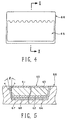
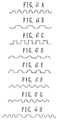
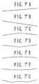
- wave forms include those as shown in Fig. 4 and Figs. 6A to 6H, such as a form consisting of repetition of a semicircle or a part of an ellipse, a form consisting of repetition of a rectangle or other polygons having or not having a round corner, and a sawtooth wave form; those as shown in Figs. 7A to 7G, such as a straight line inclined toward the longitudinal direction of the card and a curve; and any combination of the above forms.
- the optical recording member 65 is embedded in the recess 67 of the card substrate 66 in such a manner that the end face a of the optical recording member 65 is not exposed from the surface of the card substrate 66.
- the adhesive layer 68 between the optical recording member 65 and the card substrate 66 is preferably provided on the end face as well as the bottom face of the optical recording member 65.
- a taper ⁇ in the end face a of the optical recording member 65 and the side face b of the recess of the card substrate 66, as shown in Fig. 6.
- Such taper ⁇ is preferably provided in at least each side in the longitudinal direction.
- Methods for preparing the above optical recording member 65 and the card substrate 66 can be classified roughly into two methods.
- the first method is to form the end face of the optical recording member and the recess of the card substrate by cutting
- the second method is to form the optical recording member and the card substrate by injection or cast molding.
- a plate having a plurality of optical recording members is first prepared each of which comprises a transparent protective layer,- a surface hard layer formed on one side of the transparent protective layer, and a layer having a pattern and an optical recording material layer formed on the other side of the transparent protective layer remote from the surface hard layer.
- This is cut into individual optical recording members having a predetermined size. At least one side in the longitudinal direction of the optical recording member is cut into a wave form. At that time, if necessary, a desired taper is provided in the end face of the optical recording member.
- a protective layer is provided in order to avoid damage to the optical recording material layer.
- the protective layer may be formed of a material having no adverse effect on the optical recording material layer, such as an acrylic, vinyl chloride, or polyester material. When a protective film is used, there is no need to provide the protective layer.
- the transparent protective layer It is important for the transparent protective layer to be formed of a material which is less likely to exhibit birefringence. Suitable materials for the transparent protective layer include polycarbonate (PC), polymethyl methacrylate (PMMA), acrylonitrile/styrene copolymer (AS), cellulose propionate (CP), cellulose acetate butyrate (CAB), polyvinyl chloride (PVC), and polyesters. Among them, an about 400 ⁇ m-thick polycarbonate (PC) layer is preferred.
- the surface hard layer provided on one side of the transparent protective layer is suitably formed of an acrylic UV-curable hard coating agent.
- Other hard coating agents such as melamine and silicone hard coating agents, may also be used.
- the hard coating agent has excellent temperature and moisture resistance and hardness high enough to cause no cracking upon bending of the card.
- the pattern layer on the other side of the transparent protective layer may be generally formed by 2P method, injection, casting, or other known methods.
- the resin used is a UV-curable resin.
- the resin used is the same as that used in the transparent protective layer.
- the pattern layer is formed closely although a gutter for cutting is provided. This is for effectively using the optical recording material.
- the optical recording material layer may be formed of a commonly used metallic optical recording material, such as a tellurium- or bismuth-based material. It may also be formed of a dye optical recording material, such as phthalocyanine- or naphthoquinone-based recording material.
- the optical recording material layer may be of ROM type as well as write-once read-many type.
- a recess in which the optical recording member is to be embedded is formed by cutting (counter sinking). At that time, at least one side in the longitudinal direction is brought to a wave form corresponding to the form of the optical recording member.
- counter sinking is carried out so that the taper of the side face of the recess corresponds to the taper of the end face of the optical recording member.
- cutting of the edge of the card substrate 66 is carried out simultaneously with the counter sinking.
- the card substrate is formed of polyvinyl chloride, ABS resin or the like.
- a four-layer structure of 0.10/0.28/0.28/0.10 mm, 0.05/0.37/0.37/0.05 mm or the like is suitable.
- 0.10 mm-thick polyvinyl chloride and 0.05 mm-thick polyvinyl chloride are transparent.
- 0.28 mm-thick polyvinyl chloride and 0.37 mm-thick polyvinyl chloride are pearlescent. In order to enhance the abrasion resistance of a print, printing is carried out on one side of the pearlescent polyvinyl chloride.
- the optical recording member is fixed into the recess of the card substrate with an adhesive.
- adhesives such as urethane, epoxy, acrylic, vinyl, and amide adhesives, may be used for this purpose. Since, however, the adhesive comes into direct contact with the optical recording material layer, it preferably has high recording sensitivity and excellent temperature and moisture resistance.
- the fixation with the adhesive is carried out by dropping an UV-curable adhesive in the recess of the card substrate, fitting the optical recording member into the recess, pressing the optical recording member by means of a flat press having a size equal to that of the optical recording member, and applying ultraviolet light to the resultant assembly to adhere the optical recording member to the card substrate.
- a method which comprises previously applying a hot-melt adhesive to the optical recording member through a T-die, fitting the optical recording member into the recess, and hot-pressing the optical recording member by means of a flat press or a roll press may also be used.
- pressing conditions are set so that the adhesive is spread between the end face of the optical recording member and the side face of the recess of the card substrate.
- a pressure-sensitive adhesive is used for fixing the optical recording member into the recess of the card substrate, a pressure-sensitive adhesive double coated tape may be used.
- an optical recording member comprising a transparent protective layer, a surface hard layer provided on one side of the transparent protective layer, and a pattern layer and an optical recording material layer provided on the other side of the transparent protective layer is prepared, and a plastic hot-melt adhesive is coated onto the optical recording material layer.
- a plate having a plurality of optical recording members with an adhesive layer laminated thereon is cut into individual optical recording members which are then subjected to cutting in the same manner as described above.
- the optical recording member is fitted into the recess of the card substrate, and bonding is carried out by hot pressing by taking advantage of heat from a flat press or a roll press. In this case, pressing conditions are set so that the adhesive is melted and spread between the end face of the optical recording member and the side face of the recess of the card substrate.
- a transparent protective layer having a pattern is prepared using polycarbonate, acrylic, or other resins by injection or casting commonly known in the art.
- at least one side in the longitudinal direction is made wavy, and, if necessary, the whole end face is tapered.
- a surface hard layer is formed on the side of the transparent protective layer remote from the pattern, and an optical recording material layer is formed on the pattern face.
- the surface hard layer and the optical recording material layer may be the same as those described above.
- a card substrate is prepared using ABS resin, polyvinyl chloride, or other resins by injection or cast molding. At that time, a recess into which the optical recording member is to be fitted is formed.
- At least one side in the longitudinal direction is brought to a wave form corresponding to the form of the optical recording member, and, further, when the optical recording member has a tapered end face, a taper corresponding to the end face of the optical recording member is provided in the side face of the recess.
- a design is provided by in-mold decorating.
- the optical recording member is fixed into the recess of the card substrate by means of an adhesive or a pressure-sensitive adhesive in the same manner as described above.
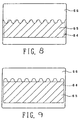
- the optical recording member 65 is embedded in an island form in the card substrate. It is also possible to use a method wherein, as shown in Fig. 8, the optical recording member 65 is embedded with both ends thereof having a trimmed-off structure. If embedding in this way is used, the recess 67 can be formed in the card substrate 66 by one-pass counter sinking even when the width of the recess 67 is large, enabling the cost to be lowered. It is noted that when TeO x or the like is used in the optical recording material layer 64, there is a possibility that oxidation starts at both edges of the optical recording member. For this reason, as shown in the hatched region of Fig. 8, no optical recording material layer 4 is preferably provided in the optical recording member in its portions near respective both ends. This offers an additional advantage that the appearance of the resultant card is like that of the card with the optical recording member embedded in an island form.
- an optical recording material layer may be omitted in an area in a wave form.
- the optical recording material layer 64 is provided in only the area other than the area in a wave form.
- the track for information recording is provided in the longitudinal direction of the card, and the area in a wave form cannot be used for information recording. Therefore, the information capacity is independently of whether or not the optical recording material layer is provided in the area in a wave form.
- the amount of the expensive optical recording material used can be reduced, and, at the same time, since the area where no optical recording material layer is provided becomes transparent, the boundary between the optical recording material layer and the area in a wave form where no information recording material layer is provided looks like a straight line, making the wave form inconspicuous.
- a magnetic stripe 69 may be provided on one side of the card substrate 66, which is the same as or opposite to the side where the optical recording member 65 is provided, or both sides of the card substrate 66, and an IC module 60 may be provided on one side of the card substrate 66 which is the same as or opposite to the side where the optical recording member 65 is provided.
- characters representing information on the cards such as personal name and registration number, can be formed as a relief of characters by embossing in the area other than that where the optical recording material is present.
- At least one side in the longitudinal direction in the optical recording member and in the recess of the card substrate in which the optical recording member is embedded are in a wave form.
- the wave form serves to disperse the stress created upon bending of the card, improving the bending strength.
- the optical card comprises: a card substrate 72 having a recess; and an optical recording member 71 comprising a transparent protective layer, a track pattern provided on the back side of the transparent protective layer, and an optical recording layer laminated so as to cover the track pattern, the optical recording member 71 being embedded in the recess of the card substrate through an adhesive layer, the optical recording member 71 being embedded in a position through which at least one of a center line x in the direction of a longer side of the card and a center line y in the direction of a shorter side of the card is passed.
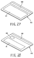
- a further improvement in bending strength can be attained when the optical recording member 71 is embedded substantially symmetrically with respect to the center line x in the direction of a longer side of the card or the center line y in the direction of a shorter side of the card. Since the bending strength in the direction of a longer side of the card is lower than that in the direction of a shorter side of the card, the bending strength is not significantly influenced by embedding of the optical recording member in a substantially symmetrical manner with respect to the center line y in the direction of a shorter side of the card, as shown in Fig. 16.
- the optical recording member 71 is embedded in the recess of the card substrate in such a manner that the end face of the optical recording member 71 is not exposed from the surface of the card substrate 72.
- the adhesive layer between the optical recording member 71 and the card substrate 72 is preferably provided on the end face as well as the bottom face of the optical recording member 71.
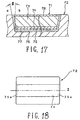
- a taper ⁇ in the end face a of the optical recording member 71 and the side face b of the recess of the card substrate 72, as shown in Fig. 17 (cross-sectional view).
- Such taper ⁇ is preferably provided in at least each side in the longitudinal direction.
- numeral 73 designates a transparent protective layer having a track pattern 74 on the underside thereof, numeral 75 an optical recording layer laminated so as to cover the track pattern 74, and numeral 76 a surface protective layer provided on the surface of the transparent protective layer 73.
- These elements constitutes the optical recording member 71.
- the optical recording member 71 is embedded in the recess 77 formed in the card substrate 72 through an adhesive layer 78.
- Methods for preparing the above optical recording member 71 and the card substrate 72 can be classified roughly into two methods.
- the first method is to form the end face a of the optical recording member 71 and the recess 77 of the card substrate 72 by cutting
- the second method is to form the optical recording member 71 and the card substrate 72 by injection or cast molding.
- a plate having a plurality of optical recording members is first prepared each of which comprises a transparent protective layer 73, a surface hard layer 76 formed on one side of the transparent protective layer 73, and a layer having a track pattern 74 and an optical recording material layer 75 formed on the other side of the transparent protective layer 73 remote from the surface hard layer.
- This is cut into individual optical recording members 71 having a predetermined size.
- a desired taper ⁇ is provided in the end face a .
- a protective layer is provided on the surface of the optical recording layer 75 in order to avoid damage to the optical recording material layer 75.
- the protective layer may be formed of a material having no adverse effect on the optical recording material layer 75, such as an acrylic, vinyl chloride, or polyester material. When a protective film is used, there is no need to provide the protective layer.
- the transparent protective layer 73 is important for the transparent protective layer 73 to be formed of a material which is less likely to exhibit birefringence.
- Suitable materials for the transparent protective layer include polycarbonate (PC), polymethyl methacrylate (PMMA), acrylonitrile/styrene copolymer (AS), cellulose propionate (CP), cellulose acetate butyrate (CAB), polyvinyl chloride (PVC), and polyesters.
- PC polycarbonate
- PMMA polymethyl methacrylate
- AS acrylonitrile/styrene copolymer
- CP cellulose propionate
- CAB cellulose acetate butyrate
- PVC polyvinyl chloride
- polyesters an about 400 ⁇ m-thick polycarbonate (PC) layer is preferred.
- the surface hard layer 76 provided on one side of the transparent protective layer 73 is suitably formed of an acrylic UV-curable hard coating agent.
- Other hard coating agents such as melamine and silicone hard coating agents, may also be used.
- the hard coating agent has excellent temperature and moisture resistance and hardness high enough to cause no cracking upon bending.
- the layer having a track pattern 74 formed on the other side of the transparent protective layer 73 may be generally formed by 2P, injection, casting, or other known methods.
- the resin used is a UV-curable resin.
- the resin used is the same as that used in the transparent protective layer 73.
- the layer having the track pattern 74 is formed closely although a gutter for cutting is provided. This is for effectively using the optical recording material.
- the optical recording layer 75 may be formed of a commonly used metallic optical recording material, such as a tellurium- or bismuth-based material. It may also be formed of a dye optical recording material, such as phthalocyanine- or naphthoquinone-based recording material.
- the optical recording material layer may be of ROM type as well as write-once read-many type.
- a recess 77 in which the optical recording member 71 is to be embedded is formed in the card substrate 72 by cutting (counter sinking).
- the recess 77 is formed in a position through which at least one of a center line x in the direction of a long side of the card and a center line y in the direction of a short side of the card is passed.
- the position of the recess 77 may be symmetrical with respect to the center line y .
- the card substrate 72 is formed of polyvinyl chloride, ABS resin or the like.
- a four-layer structure of 0.10/0.28/0.28/0.10 mm, 0.05/0.37/0.37/0.05 mm or the like is suitable.
- 0.10 mm-thick polyvinyl chloride and 0.05 mm-thick polyvinyl chloride are transparent.
- 0.28 mm-thick polyvinyl chloride and 0.37 mm-thick polyvinyl chloride are pearlescent. In order to enhance the abrasion resistance of a print, printing is carried out on one side of the pearlescent polyvinyl chloride.
- the optical recording member 71 is fixed into the recess 77 of the card substrate 72 through an adhesive layer 78.
- Known adhesives such as urethane, epoxy, acrylic, vinyl, and amide adhesives, may be used for this purpose. Since, however, the adhesive comes into direct contact with the optical recording layer 75, it preferably has high recording sensitivity and excellent temperature and moisture resistance.
- the fixation with the adhesive is carried out by dropping an UV-curable adhesive in the recess 77 of the card substrate 72, fitting the optical recording member 71 into the recess 77, pressing the optical recording member 71 by means of a flat press having a size equal to that of the optical recording member 71, and applying ultraviolet light to the resultant assembly to adhere the optical recording member 71 to the card substrate 72.
- a method which comprises previously applying a hot-melt adhesive to the optical recording member 71 through a T-die, fitting the optical recording member 71 into the recess 77, and hot-pressing the optical recording member by means of a flat press or a roll press Other methods may also be used. In all the above methods, pressing conditions are set so that the adhesive is spread between the end face a of the optical recording member 71 and the side face b of the recess of the card substrate 72.
- a pressure-sensitive adhesive is used for fixing the optical recording member 71 into the recess 77 of the card substrate 72
- a pressure-sensitive adhesive double coated tape may be used.
- an optical recording member 71 comprising a transparent protective layer 73, a surface hard layer 76 provided on one side of the transparent protective layer 73, and a layer having a track pattern 74 and an optical recording layer 75 provided on the other side of the transparent protective layer 73 is prepared, and a plastic hot-melt adhesive is coated onto the optical recording layer 75.
- a plate having a plurality of optical recording members 71 with an adhesive layer laminated thereon is cut into individual optical recording members 71 which are then subjected to cutting in the same manner as described above. Then, the optical recording member 71 is fitted into the recess 77 of the card substrate 72, and bonding is carried out by hot pressing by taking advantage of heat from a flat press or a roll press. In this case, pressing conditions are set so that the adhesive is melted and spread between the end face a of the optical recording member 71 and the side face b of the recess of the card substrate 72.
- a transparent protective layer 73 having a track pattern is prepared using polycarbonate, acrylic, or other resins by injection or cast molding commonly known in the art.
- the end face a of the transparent protective layer 73 is tapered.
- a surface hard layer 76 is formed on the side of the transparent protective layer remote from the track pattern, and an optical recording layer 75 is formed on the track pattern face.
- the surface hard layer 76 and the optical recording layer 75 may be the same as those described above.
- a card substrate 72 is prepared using ABS resin, polyvinyl chloride, or other resins by injection or casting. At that time, a recess 77 in which the optical recording member 71 is to be embedded is formed.
- the optical recording member 71 has a taper ⁇ in the end face a
- a taper corresponding to the taper ⁇ in the end face of the optical recording member 71 is provided in the side face b of the recess.
- the recess 77 of the card substrate 72 is formed in a position through which at least one of a center line x in the direction of a longer side of the card and a center line y in the direction of a shorter side of the card is passed.
- it is preferred for the position of the recess 77 to be symmetrical with respect to the center line x .
- the position of the recess 77 may be symmetrical with respect to the center line y .
- a design is provided by in-mold decorating.
- the optical recording member 71 is fixed into the recess 77 of the card substrate 72 by means of an adhesive or a pressure-sensitive adhesive in the same manner as described above.
- the optical recording member 71 is embedded in an island form in the card substrate. It is also possible to use a method wherein, as shown in Fig. 18, the optical recording member 71 is embedded in the card substrate 72 with both ends thereof having a trimmed-off structure. If embedding in this way is adopted, the recess 77 can be formed in the card substrate 72 by one-pass counter sinking even when the width of the recess 77 is large, enabling the cost to be lowered. It is noted that when TeO x or the like is used in the optical recording layer 75, there is a possibility that oxidation starts at both edges of the optical recording member. For this reason, no optical recording material layer 75 is preferably provided in the optical recording member 71 in its portions near respective both ends 71a. This offers an additional advantage that the appearance of the resultant card is like that of the card with the optical recording member embedded in an island form.
- a magnetic stripe 79 may be provided on one side of the card substrate 72, which is the same as or opposite to the side where the optical recording member 71 is provided, or both sides of the card substrate 72, and an IC module 70 may be provided on one side of the card substrate 72 which is the same as or opposite to the side where the optical recording member 71 is provided.
- characters representing information on the cards such as personal name and registration number, can be formed as a relief of characters by embossing in the area other than that where the optical recording member is present.
- the optical recording member and the recess of the card substrate in which the optical recording member is embedded are located in a position through which at least one of a center line in the direction of a longer side of the card and a center line in the direction of a shorter side of the card is passed, preventing stress created in the recess upon bending of the card from being remarkably localized.
- the optical recording member is embedded so that it is substantially symmetrical with respect to the center line in the longitudinal direction of the card, the stress created upon bending of the card can be evenly dispersed.
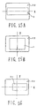
- the optical card of the present invention comprises: a card substrate; and an optical recording member, having a rectangular shape in flat, comprising a transparent protective layer, a track pattern provided on the back side of the transparent protective layer, and an optical recording layer laminated so as to cover the track pattern, the optical recording member being embedded in the card substrate with the surface of the optical recording member exposed from the card substrate, the transparent protective layer being provided with a rib portion at least on both sides thereof in the longitudinal direction of the optical recording layer with the rib portions being dropped in level from the top surface of a protrusion constituting the transparent protective layer except for the rib portions, the optical recording member being embedded and adhesive-fixed in the card substrate so that a part of the card substrate covers the rib portions and the surface of the protrusion excluding the rib portions is exposed from the card substrate.
- the optical card having the above construction can be produced by any of the following three processes.
- the first production process comprises the steps of:
- the second production process comprises the steps of:
- the third production process comprises the steps of:
- the rib portions of the optical recording member is pressed by the top sheet, preventing the optical recording member from emerging from the card substrate upon bending of the card and enabling the stress created by bending of the card to be relaxed. Therefore, there is no fear of the card substrate being folded.
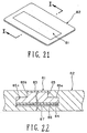
- Fig. 21 is a perspective view showing one embodiment of the present invention
- Fig. 22 is a schematic cross-sectional view taken on line X-X of Fig. 21.
- an optical recording member 81 having a rectangular shape in flat, is embedded in a card substrate 82 with the surface of the optical recording member exposed from the card substrate.
- the optical recording member 81 comprises a transparent protective layer 85, a surface hard layer 83 formed on the upper surface of the transparent protective-layer 85, a track pattern 84 formed on the lower surface of the transparent protective layer 85, and an optical recording layer 86 laminated so as to cover the track pattern 84.
- the transparent protective layer 85 is provided with a rib portion 85a on both sides thereof in the longitudinal direction of the optical recording layer with the rib portions being dropped in level from the top surface of a protrusion constituting the transparent protective layer.
- the optical recording member 81 is embedded in the card substrate 82 so that a part of the card substrate 82 covers the rib portions 85 and the surface of the protrusion 85b excluding the rib portions 85a is exposed from the card substrate 82.
- the optical recording member 81 is adhesive-fixed in the card substrate 82 through an adhesive layer 87.
- the surface of the protrusion 85b is preferably flush with the surface of the card substrate 82. However, some projection or recession is acceptable.
- the optical recording member 81 having the above construction is prepared as follows. At the outset, an optical recording member is prepared which comprises a transparent protective layer 85, a surface hard layer 83 formed on one side of the transparent protective layer 85, and a pattern layer of a track pattern 84 and an optical recording layer 86 on the other side of the transparent protective layer 85 remote from the surface hard layer 83.
- the end face of the optical recording member is cut into a desired shape having a difference in level.
- a protective layer is provided on the surface of the optical recording layer 86 in order to avoid damage to the optical recording layer 86.
- the protective layer may be formed of a material having no adverse effect on the optical recording layer 75, such as an acrylic, vinyl chloride, or polyester material. When a protective film is used, there is no need to provide the protective layer.
- the transparent protective layer 85 is important for the transparent protective layer 85 to be formed of a material which is less likely to exhibit birefringence.
- Suitable materials for the transparent protective layer include polycarbonate (PC), polymethyl methacrylate (PMMA), acrylonitrile/styrene copolymer (AS), cellulose propionate (CP), cellulose acetate butyrate (CAB), polyvinyl chloride (PVC), and polyesters.
- PC polycarbonate
- PMMA polymethyl methacrylate
- AS acrylonitrile/styrene copolymer
- CP cellulose propionate
- CAB cellulose acetate butyrate
- PVC polyvinyl chloride
- polyesters an about 400 ⁇ m-thick polycarbonate (PC) layer is preferred.
- the pattern layer formed on the other side of the transparent protective layer 85 may be generally formed by 2P method, injection, casting, or other known methods.
- the resin used is a UV-curable resin.
- the resin used is the same as that used in the transparent protective layer 85.
- the pattern layer is formed closely although a gutter for cutting is provided. This is for effectively using the optical recording material.
- the optical recording layer 86 may be formed of a commonly used metallic optical recording material, such as a tellurium- or bismuth-based material. It may also be formed of a dye optical recording material, such as phthalocyanine- or naphthoquinone-based recording material.
- the optical recording material layer may be of ROM type as well as write-once read-many type.
- the optical recording member 81 having the above construction can be prepared also by the following method.
- a transparent protective layer 85 having a track pattern 84 is prepared using polycarbonate, acrylic, or other resins by injection or casting commonly known in the art.
- the end face of the transparent protective layer 85 is cut into a desired shape having a difference in level.
- a surface hard layer 83 is formed on the side of the transparent protective layer 85 remote from the track pattern 84, and an optical recording layer 86 is formed on the track pattern face 84.
- the surface hard layer 83 and the optical recording layer 86 may be the same as those described above.
- a card substrate 82 is formed of a back sheet 111 and a top sheet 112.
- the back sheet 111 has a three-layer structure comprising a core sheet 111a formed of pearlescent polyvinyl chloride and, laminated on both sides of the core sheet 111a, an overlay sheet 111b formed of transparent polyvinyl chloride. A design or the like is printed on both sides of the core sheet 111a.
- a transparent polyvinyl chloride sheet having the same thickness as the protrusion 85b of the optical recording member 81 is used for the top sheet 112.
- a recess 113 in which the rib portions 85a and a portion located under the rib portions 85a are to be embedded is formed on the back sheet 111.
- an opening 114 having a size corresponding to the size of protrusion 81b is formed in the top sheet 112.
- the optical recording member 81 is first fixed into the recess 113 of the back sheet 111 through an adhesive layer 87.
- Known adhesives such as urethane, epoxy, acrylic, vinyl, and amide adhesives, may be used in the adhesive layer 87. Since, however, the adhesive layer 87 comes into direct contact with the optical recording layer 86, it preferably has high recording sensitivity and excellent temperature and moisture resistance.
- the fixation with the adhesive is carried out by dropping an UV-curable adhesive in the recess 113, fitting the optical recording member 81 into the recess 113, pressing the optical recording member 81 by means of a flat press having a size equal to that of the optical recording member 81, and applying ultraviolet light to the resultant assembly.
- a process which comprises previously applying a hot-melt adhesive to the optical recording member 81 through a T-die, fitting the optical recording member 81 into the recess, and hot-pressing the optical recording member by means of a flat press or a roll press.
- Other processes may also be used.
- Bonding may also be carried out with a pressure-sensitive adhesive double coated tape. Further, the following process may also be used.
- a plastic hot-melt adhesive is coated onto the optical recording layer 86.
- the optical recording member with an adhesive layer 87 laminated thereon is then cut into a desired shape.
- the optical recording member 81 is fitted into the recess 113 of the back sheet 111, and bonding is carried out by hot pressing using a flat press or a roll press.
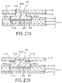
- the transparent top sheet 112 is adhered onto the top surface of the back sheet 111 so that the protrusion 81b is fit into the opening 115 of the top sheet 112.
- a method which comprises coating a hot-melt adhesive on the back side of the top sheet 112 to form an adhesive layer 115, putting the top sheet on top of the back sheet 111 and then hot-pressing the resultant assembly by means of a flat press or a roll press to carry out bonding. Since the adhesive layer 115 is not associated with the optical recording layer 86, it is possible to use an adhesive having high adhesive strength.
- top sheet 112 is formed of transparent vinyl chloride
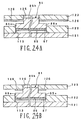
- a process may be used wherein, as shown in Fig. 23B, an adhesive layer 115 on the back side of the top sheet 112 is provided in only portions corresponding to the rib portions 85a and, in the other portions, lamination is carried out by heat fusing.
- the fixation of the optical recording member 81 into the recess 113 by bonding may be carried out simultaneously with the lamination of the top sheet 112 onto the back sheet 111.
- a card substrate 82 is formed of a back sheet 121, an intermediate sheet 122, and a top sheet 123.
- a transparent polyvinyl chloride sheet having a predetermined thickness is used as the back sheet 121
- a pearlescent polyvinyl chloride sheet having the same thickness as the rib portions 85a of the optical recording member 81 is used as the intermediate sheet 122
- a transparent polyvinyl chloride sheet having the same thickness as the protrusion 85b of the optical recording member 81 is used as the top sheet 123.
- a design or the like is printed on both sides of the intermediate sheet 122.
- An opening 124 having a size suitable for fitting the rib portions 85a of the optical recording member 81 is formed in the intermediate sheet 122, and an opening 125 having a size corresponding to the size of the protrusion 85b of the optical recording member 81 is formed in the top sheet 123. Further, an adhesive layer 126 is provided on the back side of the top sheet 123, for example, by coating a hot-melt adhesive.
- the intermediate sheet 122 and the top sheet 123 are worked.
- the intermediate sheet 122 is first put on top of the back sheet 121 and temporarily fixed thereto.
- the optical recording member 81 is fitted and temporarily fixed into the recess defined by the opening 124.
- the top sheet 123 is put on top of the intermediate sheet 122 so that the protrusion 85b of the optical recording member 81 is fitted into the opening 125.
- the whole assembly is then hot-pressed.
- the back sheet 121 is bonded to the intermediate sheet 122 by heat fusing, and the optical recording member 81 is bonded and fixed to the card substrate 82 through the adhesive layer 87 and the adhesive layer 126. Since the adhesive layer 126 is not associated with the optical recording layer 86, it is possible to use an adhesive having high adhesive strength.
- a process may also be used wherein, as shown in Fig. 24B, an adhesive layer 126 on the back side of the top sheet 123 is provided in only portions corresponding to the rib portions 85a and, in the other portions, lamination is carried out by heat fusing.
- a sheet having a three-layer structure like the back sheet 111 described above in connection with the first production method, is used as the back sheet 121, a similar design is printed thereon, and a transparent sheet is used as the intermediate sheet 122 and the back sheet 123.
- a card substrate 82 comprises a back sheet 131 and a top sheet 132.
- a pearlescent polyvinyl chloride sheet having a predetermined thickness is used as the back sheet 131
- a transparent polyvinyl chloride sheet having the same thickness as the optical recording member 81 is used as the back sheet 132
- a design or the like is previously printed on the inner side of the back sheet 131.
- a pearlescent polyvinyl chloride sheet is used as the top sheet 132
- a transparent polyvinyl chloride sheet is used as the back sheet 131
- a design or the like is printed on the inner side of the top sheet 132.
- a stepped opening 133 into which the optical recording member 81 is to be fitted from the back side of the top sheet 132 is formed in the top sheet 132.
- the optical recording member 81 is adhesive-fixed into the opening 133 through an adhesive layer 134.
- the back sheet 131 is laminated onto the back side of the top sheet 132 through an adhesive layer 87.
- the optical recording member 81 too is adhesive-fixed to the back sheet 131 through the adhesive layer 87.
- a process may also be used wherein, as shown in Fig. 25B, an adhesive layer 87 on the inner side of the back sheet 83 is provided in only portions corresponding to the optical recording layer 86 and, in the other portions, lamination is carried out by heat fusing.
- the rib portions 85a formed in the transparent protective layer 85 of the optical recording member 81 may be inclined. What is required of the rib portions which have been embedded in the card substrate is to prevent the optical recording member from emerging from the card substrate upon bending of the card.
- the form of the recess formed in the card substrate 82 preferably conforms to that of the optical recording member 81. Some gap between the optical recording member and the card substrate poses little or no problem because such gap is filled with the adhesive. Further, a gap may be provided between the optical recording member 81 in its portion other than the bottom face and the card substrate 82. This gap serves as a reservoir for the adhesive at the time of bonding of the optical recording member 81. The presence of the adhesive on the side face as well as on the bottom face of the optical recording member 81 results in further improved bending strength.
- a magnetic stripe 88 may be provided on one side of the card substrate 82, which is the same as or opposite to the side where the optical recording member 81 is provided, or both sides of the card substrate 82, and an IC module 89 may be provided on one side of the card substrate 82 which is the same as or opposite to the side where the optical recording member 81 is provided. Embossing may be carried out in an area other than the area where the above elements are provided.
- the transparent protective layer of the optical recording member is provided with a rib portion on both sides thereof in the longitudinal direction, the optical recording member is embedded'and fixed by bonding in the card substrate so that a part of the card substrate covers the rib portions and the surface of the protrusion excluding the rib portions is exposed from the card substrate.
- the rib portions of the optical recording member are pressed, preventing the optical recording member from emerging from the card substrate upon bending of the card.
- the optical card of the present invention has high bending strength.
- the optical recording member is embedded in a part of the card substrate, the utilization of the remaining area of the card substrate enables the preparation of optical cards in such a form that could not prepared in the prior art, for example, an optical card having a magnetic stripe on both sides thereof, an optical card having an emboss, and an optical card wherein an optical recording member and an IC module are provided on different sides of the card.
- a hard coat agent (UH-001, manufactured by Toray Industries, Inc.) was spin-coated on one side of a 0.4 mm-thick polycarbonate sheet (a transparent protective layer) to form a surface hard layer. Then, a guide track pattern was formed by 2P method (photo polymer method) on the other side of the sheet remote from surface hard layer. TeO x was sputtered thereon to form an optical recording material layer. Subsequently, an adhesive (PPET-2101, manufactured by Toa Gosei Chemical Industry Co.) was coated using a T-die on the optical recording material layer to form a 50 ⁇ m-thick adhesive layer. Then, cutting was carried out in such a manner that the whole end face was tapered at an angle of 10° and parallel to the card track, thereby preparing an optical recording member.
- PPET-2101 manufactured by Toa Gosei Chemical Industry Co.
- Silk offset printing was carried out on each one side of two 0.28 mm-thick pearlescent polyvinyl chloride sheets.
- the two core sheets were put on top of the other so that the non-printed faces faced each other.
- the two core sheets were sandwiched between two 0.10 mm-thick overlay sheets, and heat fusing was carried out to prepare a card substrate having a four-layer structure.
- a magnetic tape of 650 oersted was formed on one side of one of the overlay sheets, while a magnetic tape of 290 oersted was formed on one side of the other overlay sheet.
- a recess, having a rectangular shape in flat, in which the optical recording member is to be embedded was formed in the card substrate by cutting.
- the optical recording member was fitted into the recess of the card substrate, and hot pressing was carried out using a flat press having a size equal to the size of the optical recording member under conditions of 120°C and 6 kg/cm 2 for 2.5 sec. This melted the adhesive, and the melt could cover the bottom face and end face of the optical recording member to adhesive-fix the optical recording member into the recess. Further, since heat was transferred from the top of the transparent protective layer (polycarbonate) toward the polyvinyl chloride located at the bottom face of the optical recording member, sagging of the polyvinyl chloride derived from heat was not observed.
- the above sample was used to write data of 100 tracks by optical card R/W (3B3H-DJ-01, manufactured by Omron Corp.). As a result, the error rate was within 1 x 10 -4 . Further, even after embossing on the card substrate of the above sample, writing and reading by optical card R/W could be successfully carried out. Furthermore, the above sample was tested for bending according to bending test specifications of ISO. As a result, no problem occurred.
- a 0.4 mm-thick patterned polymethyl methacrylate (a surface protective layer) was prepared by casting.
- the casting was designed so that the whole end face was tapered at an angle of 10°.
- a hard coat agent (UH-001, manufactured by Toray Industries, Inc.) was spin-coated on the side of the surface protective layer remote from the pattern face to form a surface hard layer. TeO x was sputtered on the pattern face to form an optical recording material layer, thereby preparing an optical recording member.
- a card substrate in the form of a 0.78 mm-thick card having in a part thereof a recess having a depth of 0.45 mm and an outer diameter of 16 mm x 84 mm, the side face of the recess being tapered at an angle of 10° was prepared using ABS resin by injection molding.
- a design was formed by in-mold decorating.
- a UV-curable adhesive (863, manufactured by Kyoritsu Chemical Industry Corporation) was dropped in the recess of the card substrate, and the optical recording member was fitted into the recess. The whole assembly was pressed by a flat press and irradiated with ultraviolet light to cure an adhesive. At that time, press conditions were set so that the adhesive was spread also on the end face of the optical recording member.
- the above sample was used to write data of 100 tracks by optical card R/W (3B3H-DJ-01, manufactured by Omron Corp.). The error rate was within 1 x 10 -4 . Further, the above sample was tested for bending according to bending test specifications of ISO. As a result, no problem occurred.
- the present invention having the above constitution has the following effects.
- the end face of the optical recording member and the side face of the recess of the card substrate are tapered outwardly so that the taper in the face of the optical recording member faces the taper in the side face of the recess of the card substrate.
- the optical recording member is embedded in the recess of the card substrate so as for the end face of the optical recording member not to be exposed from the card substrate. This permits the optical recording member to be easily embedded into the recess and can minimize the gap between the end face of the optical recording member and the side face of the recess, offering good appearance.
- the optical card Since the adhesive layer between the optical recording member and the card substrate is provided on the end face as well as on the bottom face, the optical card has improved bending strength.
- the optical recording member is embedded in a part of the card substrate, the utilization of the remaining area of the card substrate enables the preparation of optical cards in such a form that could not prepared in the prior art, for example, an optical card having a magnetic stripe on both sides thereof, an optical card having an emboss, an optical card wherein an optical recording member and an IC module are provided on different sides of the card, an optical card both sides of which can be subjected to CP working, and an optical card wherein a hologram can be transferred onto both sides thereof.
- a hard coat agent (UH-001, manufactured by Toray Industries, Inc.) was spin-coated on one side of a 0.4 mm-thick polycarbonate sheet (a transparent protective layer) to form a surface hard layer. Then, a guide track pattern was formed by 2P method on the other side of the sheet remote from the surface hard layer. TeO x was sputtered thereon to form an optical recording material layer. Subsequently, an adhesive (PPET-2101, manufactured by Toa Gosei Chemical Industry Co.) was coated using a T-die on the optical recording material layer to form a 50 ⁇ m-thick adhesive layer. Then, cutting was carried out so that a wave form (shown in Fig.
- the same wave form as that provided in the optical recording member was formed on one upper side in the longitudinal direction of the recess, and counter sinking was carried out in such a manner that the side face of the recess was tapered outwardly at an angle of 10° to the direction normal to the bottom face of the card and the size of the recess was 50 ⁇ m larger than the optical recording member. Further, cutting of the end face of the card substrate was carried out so as to ensure the parallelism between the recess and the end face of the card substrate.
- the optical recording member was fitted into the recess of the card substrate, and hot pressing was carried out using a flat press having a size equal to the size of the optical recording member under conditions of 120°C and 6 kg/cm 2 for 2.5 sec. melted the adhesive, and bonding could be carried out with the melt covering the bottom face and end face of the optical recording member. Further, since heat was transferred from the top of the transparent protective layer (polycarbonate) toward the polyvinyl chloride located on the bottom face of the optical recording member, sagging of the polyvinyl chloride derived from heat was not observed.
- optical card thus prepared was used to write data of 100 tracks by optical card R/W (3B3H-DJ-01, manufactured by Omron Corp.). As a result, the error rate was within 1 x 10 -4 . Further, even after embossing on the card substrate, writing and reading by optical card R/W could be successfully carried out. Furthermore, the optical card was tested for bending according to bending test specifications of ISO. As a result, no problem occurred.
- a 0.4 mm-thick patterned polymethyl methacrylate (a surface protective layer) was prepared by casting.
- design was carried out so that a wave form (shown in Fig. 4) having a width of 3 mm, a pitch of 4 mm and a corner R of 1 mm was formed on the top in the longitudinal direction was formed and the end face was tapered at an angle of 10°.
- a hard coat agent (UH-001, manufactured by Toray Industries, Inc.) was spin-coated on the side of the surface protective layer remote from the pattern face to form a surface hard layer. TeO x was sputtered on the pattern face to form an optical recording material layer, thereby preparing an optical recording member.
- a card substrate in a 0.78 mm-thick card form having a recess in which the optical recording member is to be embedded was formed using ABS resin by injection molding.
- the recess was formed so that the depth was 0.45 mm, the same wave form as that of the optical recording member was provided on one upper side in the longitudinal direction, the side face was tapered outwardly at an angle of 10° to the direction normal to the bottom face of the card and the outer dimension was 16 mm x 84 mm.
- a design was formed by in-mold decorating.
- a UV-curable adhesive (863, manufactured by Kyoritsu Chemical Industry Corporation) was dropped in the recess of the card substrate, and the optical recording member was fitted into the recess. The whole assembly was pressed by a flat press and irradiated with ultraviolet light to cure the adhesive. Press conditions were set so that the adhesive was spread also on the end face of the optical recording member.
- the optical card thus prepared was used to write data of 100 tracks by optical card R/W (3B3H-DJ-01, manufactured by Omron Corp.). As a result, the error rate was within 1 x 10 -4 . Further, the optical card was tested for bending according to bending test specifications of ISO. As a result, no problem occurred.
- the present invention having the above constitution has the following effects.
- At least one side in the longitudinal direction is in a wave form, which serves to disperse the bending stress created upon bending of the card, improving the bending strength.
- the optical card Since the adhesive layer between the optical recording member and the card substrate is provided on the end face as well as on the bottom face of the optical recording member, the optical card has further improved bending strength.
- the optical recording member can be easily fitted into the recess and, at the same time, the gap between the end face of the optical recording member and the side face of the recess of the card substrate can be minimized, offering good appearance.
- the optical recording member is embedded in a part of the card substrate, the utilization of the remaining area of the card substrate enables the preparation of optical cards in such a form that could not be prepared in the prior art, for example, an optical card having a magnetic stripe on both sides thereof, an optical card having an emboss, an optical card wherein an optical recording member and an IC module are provided on different sides of the card, an optical card both sides of which can be subjected to CP working, and an optical card wherein a hologram can be transferred onto both sides thereof.
- a hard coat agent (UH-001, manufactured by Toray Industries, Inc.) was spin-coated on one side of a 0.4 mm-thick polycarbonate sheet (a transparent protective layer) to form a surface hard layer. Then, a guide track pattern was formed by 2P method on the other side of the sheet remote from surface hard layer. TeO x was sputtered thereon to form an optical recording layer. Subsequently, an adhesive (PPET-2101, manufactured by Toa Gosei Chemical Industry Co.) was coated using a T-die on the optical recording layer to form a 50 ⁇ m-thick adhesive layer. Then, cutting was carried out in such a manner that the end face was tapered at an angle of 10° and parallel to the card track, thereby preparing an optical recording member having a size of 15 mm in width and 80 mm in length.
- PPET-2101 manufactured by Toa Gosei Chemical Industry Co.
- counter sinking was carried out in such a manner that the side face of the recess was tapered outwardly at an angle of 10° to the direction normal to the bottom face of the card and the size of the recess was 50 ⁇ m larger than the optical recording member. Further, cutting of the end face of the card substrate was carried out so as to ensure the parallelism between the recess and the end face of the card substrate. In this case, counter sinking was carried out so that the recess was positioned at the center of the card substrate.
- the optical recording member was fitted into the recess of the card substrate, and hot pressing was carried out using a flat press having a size equal to the size of the optical recording member under conditions of 120°C and 6 kg/cm 2 for 2.5 sec. This melted the adhesive, and bonding could be carried out with the melt covering the bottom face and end face of the optical recording member. Further, since heat was transferred from the top of the transparent protective layer (polycarbonate) toward the polyvinyl chloride located on the bottom face of the optical recording member, sagging of the polyvinyl chloride derived from heat was not observed.
- the optical card prepared above was tested for bending according to bending test specifications of ISO. As a result, no problem occurred.
- a 0.4 mm-thick patterned polymethyl methacrylate (a surface protective layer) was prepared by casting. In this case, design was carried out so that the end face was tapered at an angle of 10°. Then, a hard coat agent (UH-001, manufactured by Toray Industries, Inc.) was spin-coated on the side of the surface protective layer remote from the pattern face to form a surface hard layer. TeO x was sputtered on the pattern face to form an optical recording layer, thereby preparing an optical recording member. The size of the optical recording member was 10 mm in width and 50 mm in length.
- a card substrate in a 0.78 mm-thick card form having a recess in which the optical recording member is to be embedded was formed using ABS resin by injection molding.
- the recess was formed so that the depth was 0.45 mm, the side face was tapered outwardly at an angle of 10° to the direction normal to the bottom face of the card as in the case of the optical recording member.
- a design was provided by in-mold decorating. As shown in Fig. 28, the recess was formed in a position which was substantially symmetrical with respect to the center line in the longitudinal direction of the card substrate and closer to one short side than the other short side.
- a UV-curable adhesive (863, manufactured by Kyoritsu Chemical Industry Corporation) was then dropped in the recess of the card substrate, and the optical recording member was fitted into the recess. The whole assembly was pressed by a flat press and irradiated with ultraviolet light to cure the adhesive. Press conditions were set so that the adhesive was spread also on the end face of the optical recording member. Further, an IC module was embedded in a position adjacent to the optical recording member.
- the optical card thus prepared was tested for bending according to bending test specifications of ISO as in the case of the above examples. As a result, no problem occurred.
Landscapes
- Engineering & Computer Science (AREA)
- Physics & Mathematics (AREA)
- General Physics & Mathematics (AREA)
- Theoretical Computer Science (AREA)
- Computer Hardware Design (AREA)
- Microelectronics & Electronic Packaging (AREA)
- Credit Cards Or The Like (AREA)
- Optical Record Carriers And Manufacture Thereof (AREA)
Claims (27)
- Optische Karte, aufweisend: ein Kartensubstrat (6; C; 66; 72; 82) mit einer Ausnehmung (7; 67; 77); und ein optisches Aufzeichnungselement (5; H; 65; 71; 81) umfassend, in der folgenden Reihenfolge, eine harte Oberflächenschicht (1; 61; 81), eine lichtdurchlässige bzw. transparente Schutzschicht (2; 63; 73; 85), eine Musterschicht (3) und eine optische Aufzeichnungsmaterialschicht (4; 64), wobei das optische Aufzeichnungselement (5; H; 65; 71; 81) in der Ausnehmung (7; 67; 77) durch eine Klebemittel- bzw. Klebstoffschicht (8; 68; 78; 87) in der Weise eingebettet ist, dass die optische Aufzeichnungsmaterialschicht (4; 64) in Berührung mit der Klebemittelschicht (8; 68; 78; 87) ist,
wobei die Endfläche (a) des optischen Aufzeichnungselements (5; H; 65; 71; 81) und die Seitenfläche (b) der Ausnehmung(7; 67; 77) des Kartensubstrats (6; C; 66; 72; 82) jeweils sich auswärts erweiternde bzw. ausweitende, einander gegenüberliegende Konizitäten bzw. Verjüngungen (α) aufweisen und wobei das optische Aufzeichnungselement (5; H; 65; 71; 81) in der Ausnehmung (7; 67; 77) des Kartensubstrats (6; C; 66;72; 82) in der Weise eingebettet ist, dass die Endfläche (a) des optischen Aufzeichnungselements (5; H; 65; 71; 81) von dem Kartensubstrat (6; C; 66; 72; 82) nicht freiliegend bzw. freigelegt bzw. exponiert ist,
dadurch gekennzeichnet, dass die Endfläche (a) des optischen Aufzeichnungselements (5; H; 65; 71; 81) und die Seitenfläche (b) der Ausnehmung (7; 67; 77) des Kartensubstrats (6; C; 66; 72; 82) jeweils unter einem Winkel von 3 bis 50° zu der Richtung normal zu der Oberfläche der Karte konisch bzw. kegelförmig zulaufend bzw. verjüngt sind. - Optische Karte nach Anspruch 1, bei der die Klebemittelschicht (8; 68; 78; 87) sowohl an der Endfläche (a) als auch an der unteren Fläche des optischen Aufzeichnungselements vorgesehen ist.
- Optische Karte nach Anspruch 1, bei der die Endfläche (a) des optischen Aufzeichnungselements (5; H; 65; 71; 81) und die Ausnehmung (7; 67; 77) des Kartensubstrats (6; C; 66; 72; 82) durch Schneiden bzw. Abtragen bzw. Fräsen bearbeitet worden sind.
- Optische Karte nach Anspruch 1, bei der das optische Aufzeichnungselement (5; H; 65; 71; 81) und das Kartensubstrat (6; C; 66; 72; 82) durch Spritzguss- oder Gießformen hergestellt worden sind.
- Optische Karte nach Anspruch 1, bei der ein Magnetstreifen (9; 69; 79) an einer von beiden Seiten des Kartensubstrats (6; C; 66; 72; 82) vorgesehen ist, welche die gleiche Seite wie die Seite oder die gegenüberliegende bzw. entgegengesetzte Seite zu der Seite ist, an der das optische Aufzeichnungselement (5; H; 65; 71; 81) vorgesehen ist, oder an beiden Seiten des Kartensubstrats (6; C; 66; 72; 82) vorgesehen ist.
- Optische Karte nach Anspruch 1, bei der ein IC-Modul bzw. Flachbaugruppe mit integriertem Schaltkreis (10; 70) an einer Seite des Kartensubstrats (6; C; 66; 72; 82) vorgesehen ist, die die gleiche wie die Seite oder die gegenüberliegende bzw. entgegengesetzte Seite zu dieser Seite ist, an der das optische Aufzeichnungselement (5; H; 65; 71; 81) vorgesehen ist.
- Optische Karte nach Anspruch 1, bei der die Härte des optischen Aufzeichnungselements (5; H; 65; 71; 81) im wesentlichen die gleiche wie diejenige des Kartensubstrats (6; C; 66; 72; 82) ist.
- Optische Karte nach einem oder mehreren der vorhergehenden Ansprüche, bei der wenigstens eine Seite in der Längsrichtung eines jeden der beiden, nämlich des optischen Aufzeichnungselements (65) und der Ausnehmung (67) des Kartensubstrats (66) in einer Wellenform ist.
- Optische Karte nach Anspruch 8, bei der die Klebemittelschicht (68) zwischen dem optischen Aufzeichnungselement (65) und dem Kartensubstrat (66) sowohl an der Endfläche (a) als auch an der unteren Fläche des optischen Aufzeichnungselements (65) vorgesehen ist.
- Optische Karte nach Anspruch 8, bei der sowohl die Endfläche (a) des optischen Aufzeichnungselements (65) als auch die Seitenfläche (b) in der Ausnehmung (67) des Kartensubstrats (66) kegelförmig bzw. konisch zulaufend bzw. verjüngt sind.
- Optische Karte nach Anspruch 8, bei der eine Prägung bzw. Einprägung in einem Bereich vorgesehen ist, der von dem Bereich verschieden ist, in dem das optische Aufzeichnungselement (65) vorhanden ist.
- Optische Karte nach Anspruch 8, bei der das optische Aufzeichnungselement (65) in einer Position eingebettet ist, durch die wenigstens eine der folgenden Mittellinien, nämlich eine Mittellinie (x) in der Richtung einer längeren Seite der Karte und eine Mittellinie (y) in der Richtung einer kürzeren Seite verläuft.
- Optische Karte nach einem oder mehreren der vorhergehenden Ansprüche, bei der die transparente Schutzschicht (85) mit einem Rippenbereich (85a) mindestens an beiden Seiten von ihr in der Längsrichtung versehen ist, wobei die Rippenbereiche (85a) im Niveau von der Oberseite eines Vorsprunges (85b) nach unten abgesetzt bzw. versenkt sind, der die transparente Schutzschicht (85) mit Ausnahme der Rippenbereiche (85a) bildet, wobei das optische Aufzeichnungselement (81) in dem Kartensubstrat (82) in der Weise eingebettet ist, dass ein Teil des Kartensubstrats (82) die Rippenbereiche (85a) bedeckt und die Oberfläche des Vorsprungs (85b) mit Ausnahme der Rippenbereiche (85a) von dem Kartensubstrat (82) freiliegend bzw. freigelegt bzw. exponiert ist.
- Optische Karte nach einem oder mehreren der vorhergehenden Ansprüche, bei der ein Spur- bzw. Speicherspur-Muster (74) an der Rückseite der transparenten Schutzschicht (73) vorgesehen ist und bei der die optische Aufzeichnungsschicht (75) in der Weise laminiert bzw. geschichtet ist, dass sie das Spur- bzw. Speicherspurmuster (74) bedeckt bzw. abdeckt, wobei das optische Aufzeichnungselement (71) in einer Position eingebettet ist, durch die wenigstens eine der folgenden Mittellinien, nämlich eine Mittellinie (x) in der Richtung einer längeren Seite der Karte und eine Mittellinie (y) in der Richtung einer kürzeren Seite verläuft.
- Optische Karte nach Anspruch 14, bei der das optische Aufzeichnungselement (71) im wesentlichen symmetrisch in Bezug auf die Mittellinie (x) in der Richtung einer längeren Seite der Karte eingebettet ist.
- Optische Karte nach Anspruch 14, bei der das optische Aufzeichnungselement (71) im wesentlichen symmetrisch in Bezug auf die Mittellinie (y) in der Richtung einer kürzeren Seite der Karte eingebettet ist.
- Optische Karte nach Anspruch 14, bei der die Klebemittelschicht (78) zwischen dem optischen Aufzeichnungselement (71) und dem Kartensubstrat (72) sowohl an der Endfläche (a) als auch an der unteren Fläche des optischen Aufzeichnungselements (71) vorgesehen ist.
- Optische Karte nach Anspruch 14, bei der die Endfläche (a) des optischen Aufzeichnungselements (71) und die Seitenfläche (b) in der Ausnehmung (77) des Kartensubstrats(72) kegelförmig bzw. konisch zulaufend bzw. verjüngt sind.
- Optische Karte nach Anspruch 14, bei der eine Prägung bzw. Einprägung in einem Bereich vorgesehen ist, der von dem Bereich verschieden ist, in dem das optische Aufzeichnungselement (71) vorgesehen ist.
- Verfahren zum Herstellen einer optischen Karte gemäß Anspruch 13, wobei das Verfahren die folgenden Schritte aufweist:Herstellen einer rückseitigen Platte (111) und einer oberen Platte (112) zum Bilden des Kartensubstrats (82);Bilden einer Ausnehmung (113) in der rückseitigen Platte (111), wobei in dieser Ausnehmung (113) die Rippenbereiche (85a) und ein Bereich in einer niedrigeren Position als die Rippenbereiche des optischen Aufzeichnungselements (81) einzubetten und zu bilden sind, und Bilden einer Öffnung (114) in der oberen Platte (112), welche die gleiche Dicke wie der Vorsprung (85b) des optischen Aufzeichnungselements (81) aufweist, wobei die Öffnung (114) eine dem Vorsprung (85b) entsprechende Größe bzw. Abmessung aufweist; undBefestigen des optischen Aufzeichnungselements (81) mittels Klebstoff bzw. Klebemittel oder Einpassen bzw. Einfügen des optischen Aufzeichnungselements (81) in der oder die Ausnehmung (113) der rückseitigen Platte (111), Anbringen bzw. Aufbringen der oberen Platte (112) auf die obere Seite der rückseitigen Platte (111), derart, dass der Vorsprung (85b) des optischen Aufzeichnungselements (81) in die Öffnung (114) eingepasst bzw. eingefügt wird, und Verbinden bzw. Zusammenfügen und Integrieren der rückseitigen Platte (111) mit der oberen Platte (112) durch Verkleben oder Heißschmelzen, um hierdurch eine optische Karte herzustellen, dadurch gekennzeichnet, dass der Schritt des Bildens einer Ausnehmung (113) den Schritt aufweist, die Seitenfläche der Ausnehmung unter einem Winkel von 3 bis 50° zu der Richtung normal zu der Oberfläche der Karte kegelförmig bzw. konisch verlaufend auszubilden bzw. zu verjüngen.
- Verfahren zum Herstellen einer optischen Karte gemäß Anspruch 13, wobei das Verfahren die folgenden Schritte aufweist:Herstellen einer rückseitigen Platte (121), einer Zwischenplatte (122) und einer oberen Platte (123) zum Bilden des Kartensubstrats (59);Bilden einer Öffnung in der Zwischenschicht (122), die dieselbe Dicke wie die Rippenbereiche (85a) des optischen Aufzeichnungselements (81) aufweist, wobei die Öffnung eine Größe bzw. Abmessung aufweist, die zum Einpassen bzw. Einfügen der Rippenbereiche (85a) hierin geeignet ist, und Bilden einer Öffnung (125) in der oberen Platte (123) mit derselben Dicke wie der Vorsprung (85b) des optischen Aufzeichnungselements (81), wobei die Öffnung (125) eine dem Vorsprung (85b) entsprechende Größe bzw. Abmessung aufweist;Anbringen bzw. Aufbringen der rückseitigen Platte (121) und der Zwischenplatte (122) an der oberen Seite der anderen und Einpassen bzw. Einfügen des optischen Aufzeichnungselements (81) in eine Ausnehmung, die durch die Öffnung der Zwischenplatte definiert ist; undAnbringen bzw. Aufbringen der oberen Platte (123) auf die obere Seite der Zwischenplatte (122), derart, dass der Vorsprung (85b) des optischen Aufzeichnungselements (81) in die Öffnung (125) der oberen Platte (123) einzupassen bzw. einzufügen ist, und Verbinden bzw. Zusammenfügen und Integrieren der Elemente miteinander durch Verkleben oder Heißverschmelzen, um hierdurch eine optische Karte herzustellen, dadurch gekennzeichnet, dass der Schritt des Bildens einer Öffnung den Schritt aufweist, die Seitenfläche der Öffnung unter einem Winkel von 3 bis 50° zu der Richtung normal zu der Oberfläche der Karte kegelförmig bzw. konisch verlaufend auszubilden bzw. zu verjüngen.
- Verfahren zum Herstellen einer optischen Karte gemäß Anspruch 1, wobei das Verfahren die folgenden Schritte aufweist:Herstellen einer rückseitigen Platte (131) und einer oberen Platte (132) zum Bilden des Kartensubstrats (15);Bilden einer abgestuften Öffnung (133) in der oberen Platte (132) mit der gleichen Dicke wie das optische Aufzeichnungselement (81), wobei in die abgestufte Öffnung (133) das optische Aufzeichnungselement (81) von der Rückseite der oberen Platte (132) einzupassen bzw. einzufügen ist;Befestigen des optischen Aufzeichnungselements (81) in der Öffnung (133) mittels Klebstoff bzw. Klebemittel; undLaminieren bzw. Schichten der rückseitigen Platte (131) auf der Rückseite der oberen Platte (132), um eine optische Karte herzustellen, dadurch gekennzeichnet, dass der Schritt des Formens einer Öffnung den Schritt aufweist, die Seitenfläche der Öffnung unter einem Winkel von 3 bis 50° zu der Richtung normal zu der Oberfläche der Karte kegelförmig bzw. konisch verlaufend auszubilden bzw. zu verjüngen.
- Verfahren nach Anspruch 21, bei dem ein Druck bzw. Aufdruck an der oberen Seite oder der inneren Seite der Zwischenplatte (122) vorgesehen ist, um die Rippenbereiche (85a) verborgen zu halten, so dass das Vorhandensein der Rippenbereiche (85a) von der Außenseite der Karte nicht erkannt wird.
- Verfahren nach einem der Ansprüche 20 bis 22, bei dem ein Druck bzw. Aufdruck an wenigstens einer Seite der rückseitigen Platte (111; 121; 131) vorgesehen ist und die obere Platte (112; 123; 132) lichtdurchlässig bzw. transparent ist.
- Verfahren nach einem der Ansprüche 20 bis 22, bei dem ein Druck bzw. Aufdruck an der oberen Seite oder der inneren Seite der oberen Platte (112; 123; 132) vorgesehen ist, um die Rippenbereiche (85a) verborgen zu halten, so dass das Vorhandensein der Rippenbereiche (85a) von der Außenseite der Karte nicht erkannt wird.
- Verfahren nach einem der Ansprüche 20 oder 21, bei dem die obere Platte (112; 123) undurchsichtig gemacht ist, um die Rippenbereiche (85a) verborgen zu halten, so dass das Vorhandensein der Rippenbereiche (85a) von der Außenseite der Karte nicht erkannt wird.
- Verfahren nach einem der Ansprüche 20 bis 22, bei dem kein optisches Aufzeichnungsmaterial in einem den Rippenbereichen (85a) entsprechenden Bereich gebildet wird, so dass das Vorhandensein der Rippenbereiche (85a) von der Außenseite der Karte nicht erkannt wird.
Applications Claiming Priority (12)
| Application Number | Priority Date | Filing Date | Title |
|---|---|---|---|
| JP192269/94 | 1994-07-25 | ||
| JP6192269A JPH0834184A (ja) | 1994-07-25 | 1994-07-25 | 光カード |
| JP19226994 | 1994-07-25 | ||
| JP203012/94 | 1994-08-05 | ||
| JP6203012A JPH0850640A (ja) | 1994-08-05 | 1994-08-05 | 光カード |
| JP20301294 | 1994-08-05 | ||
| JP27008494 | 1994-11-04 | ||
| JP270084/94 | 1994-11-04 | ||
| JP6270084A JPH08132772A (ja) | 1994-11-04 | 1994-11-04 | 光カード |
| JP27528694A JP3501522B2 (ja) | 1994-11-09 | 1994-11-09 | 光カード及びその製造方法 |
| JP27528694 | 1994-11-09 | ||
| JP275286/94 | 1994-11-09 |
Publications (3)
| Publication Number | Publication Date |
|---|---|
| EP0694873A2 EP0694873A2 (de) | 1996-01-31 |
| EP0694873A3 EP0694873A3 (de) | 1996-05-01 |
| EP0694873B1 true EP0694873B1 (de) | 2003-01-22 |
Family
ID=27475583
Family Applications (1)
| Application Number | Title | Priority Date | Filing Date |
|---|---|---|---|
| EP95111718A Expired - Lifetime EP0694873B1 (de) | 1994-07-25 | 1995-07-25 | Optische Karte |
Country Status (3)
| Country | Link |
|---|---|
| US (1) | US5763868A (de) |
| EP (1) | EP0694873B1 (de) |
| DE (1) | DE69529440T2 (de) |
Families Citing this family (34)
| Publication number | Priority date | Publication date | Assignee | Title |
|---|---|---|---|---|
| US6070990A (en) * | 1997-05-02 | 2000-06-06 | Eveready Battery Company, Inc. | Card light having a cover being an adhesively attached label |
| DE19721058A1 (de) * | 1997-05-20 | 1998-11-26 | Giesecke & Devrient Gmbh | Spritzgußkarte mit Dekorschicht |
| FR2785072B1 (fr) * | 1998-10-23 | 2001-01-19 | St Microelectronics Sa | Circuit electronique autocollant |
| US6484940B1 (en) * | 1999-05-11 | 2002-11-26 | Digital Castles | Data storage card having both linear and annular data regions |
| US6923378B2 (en) * | 2000-12-22 | 2005-08-02 | Digimarc Id Systems | Identification card |
| TWI242206B (en) * | 2001-06-22 | 2005-10-21 | Fuji Photo Film Co Ltd | Optical information recording medium |
| US7341820B2 (en) * | 2001-11-30 | 2008-03-11 | Fujifilm Corporation | Optical information recording medium |
| WO2003052680A1 (en) | 2001-12-18 | 2003-06-26 | Digimarc Id System, Llc | Multiple image security features for identification documents and methods of making same |
| AU2002364746A1 (en) | 2001-12-24 | 2003-07-15 | Digimarc Id Systems, Llc | Systems, compositions, and methods for full color laser engraving of id documents |
| US7694887B2 (en) | 2001-12-24 | 2010-04-13 | L-1 Secure Credentialing, Inc. | Optically variable personalized indicia for identification documents |
| AU2002361855A1 (en) * | 2001-12-24 | 2003-07-15 | Digimarc Id Systems Llc | Pet based multi-multi-layer smart cards |
| US7207494B2 (en) | 2001-12-24 | 2007-04-24 | Digimarc Corporation | Laser etched security features for identification documents and methods of making same |
| AU2002364255A1 (en) | 2001-12-24 | 2003-07-15 | Digimarc Id Systems, Llc | Covert variable information on id documents and methods of making same |
| US7728048B2 (en) | 2002-12-20 | 2010-06-01 | L-1 Secure Credentialing, Inc. | Increasing thermal conductivity of host polymer used with laser engraving methods and compositions |
| TW200303015A (en) * | 2002-01-23 | 2003-08-16 | Fuji Photo Film Co Ltd | Method for producing optical information recording medium and optical information recording medium |
| WO2003088144A2 (en) | 2002-04-09 | 2003-10-23 | Digimarc Id Systems, Llc | Image processing techniques for printing identification cards and documents |
| US7140540B2 (en) * | 2002-05-08 | 2006-11-28 | Lasercard Corporation | Method of making secure personal data card |
| US7824029B2 (en) | 2002-05-10 | 2010-11-02 | L-1 Secure Credentialing, Inc. | Identification card printer-assembler for over the counter card issuing |
| US7185814B2 (en) * | 2002-10-16 | 2007-03-06 | Dcard, Inc. | Layer structure and method of manufacture for optical memory strip (OMS) |
| US7334733B2 (en) * | 2002-10-16 | 2008-02-26 | Dcard, Inc. | Data access device using rotational head to access data stored in data strips and data arc segments or data circles |
| US7804982B2 (en) | 2002-11-26 | 2010-09-28 | L-1 Secure Credentialing, Inc. | Systems and methods for managing and detecting fraud in image databases used with identification documents |
| CN100341059C (zh) * | 2002-12-19 | 2007-10-03 | 富士胶片株式会社 | 光信息记录方法及光信息记录介质 |
| ATE491190T1 (de) | 2003-04-16 | 2010-12-15 | L 1 Secure Credentialing Inc | Dreidimensionale datenspeicherung |
| US20050072849A1 (en) * | 2003-09-03 | 2005-04-07 | Jones Robert L. | Identification document with optical memory and related method of manufacture |
| US20060208062A1 (en) * | 2005-03-16 | 2006-09-21 | Osborn Warren R | Injection molded gift case for debit, credit and smart cards |
| KR100717044B1 (ko) * | 2005-10-18 | 2007-05-10 | 삼성전자주식회사 | 광기록 매체가 매립된 광기록 메모리 |
| US12121328B2 (en) | 2007-12-24 | 2024-10-22 | Dynamics Inc. | Credit, security, debit cards and the like with buttons |
| US9418524B2 (en) * | 2014-06-09 | 2016-08-16 | Tyco Fire & Security Gmbh | Enhanced signal amplitude in acoustic-magnetomechanical EAS marker |
| US9831724B2 (en) | 2014-12-02 | 2017-11-28 | Tyco Fire & Security Gmbh | Access control system using a wearable access sensory implementing an energy harvesting technique |
| US9384607B1 (en) | 2014-12-03 | 2016-07-05 | Tyco Fire & Security Gmbh | Access control system |
| ES2833015T3 (es) | 2014-12-02 | 2021-06-14 | Sensormatic Electronics Llc | Etiquetas RFID pasivas con circuitos integrados que utilizan tecnología de subumbral |
| US9384608B2 (en) | 2014-12-03 | 2016-07-05 | Tyco Fire & Security Gmbh | Dual level human identification and location system |
| US9710978B1 (en) | 2016-03-15 | 2017-07-18 | Tyco Fire & Security Gmbh | Access control system using optical communication protocol |
| US9824559B2 (en) | 2016-04-07 | 2017-11-21 | Tyco Fire & Security Gmbh | Security sensing method and apparatus |
Family Cites Families (13)
| Publication number | Priority date | Publication date | Assignee | Title |
|---|---|---|---|---|
| DE3248385A1 (de) * | 1982-12-28 | 1984-06-28 | GAO Gesellschaft für Automation und Organisation mbH, 8000 München | Ausweiskarte mit integriertem schaltkreis |
| DE3650414T2 (de) * | 1985-02-18 | 1996-06-20 | Dainippon Printing Co Ltd | Prozess zum Herstellen von optischen Datenkarten. |
| FR2625000B1 (fr) * | 1987-12-22 | 1991-08-16 | Sgs Thomson Microelectronics | Structure de carte a puce |
| US4812633A (en) * | 1988-04-08 | 1989-03-14 | Minnesota Mining And Manufacturing Company | Optical data card |
| US5208450A (en) * | 1988-04-20 | 1993-05-04 | Matsushita Electric Industrial Co., Ltd. | IC card and a method for the manufacture of the same |
| DE68923686T2 (de) * | 1988-04-20 | 1996-01-25 | Matsushita Electric Ind Co Ltd | Halbleiterkarte und verfahren zur herstellung. |
| JPH0641760Y2 (ja) | 1988-07-26 | 1994-11-02 | 株式会社アマダ | プレス機械における制御装置 |
| US5270526A (en) * | 1989-11-02 | 1993-12-14 | Nippon Conlux Co., Ltd. | Card type recording medium and method of preventing a false use thereof |
| JPH04129077A (ja) * | 1990-09-19 | 1992-04-30 | Hitachi Ltd | 光カードメモリ |
| JPH04148999A (ja) * | 1990-10-12 | 1992-05-21 | Dainippon Printing Co Ltd | Icカード |
| JPH04307297A (ja) * | 1991-04-04 | 1992-10-29 | Matsushita Electric Ind Co Ltd | Icカード |
| US5432329A (en) * | 1992-02-07 | 1995-07-11 | American Bank Note Holographics | Automated holographic optical recognition and decoding system for verification |
| GB2267683A (en) * | 1992-06-02 | 1993-12-15 | Gec Avery Ltd | Integrated circuit card or token |
-
1995
- 1995-07-25 EP EP95111718A patent/EP0694873B1/de not_active Expired - Lifetime
- 1995-07-25 DE DE69529440T patent/DE69529440T2/de not_active Expired - Fee Related
- 1995-07-25 US US08/505,525 patent/US5763868A/en not_active Expired - Fee Related
Also Published As
| Publication number | Publication date |
|---|---|
| EP0694873A2 (de) | 1996-01-31 |
| DE69529440T2 (de) | 2003-11-20 |
| DE69529440D1 (de) | 2003-02-27 |
| EP0694873A3 (de) | 1996-05-01 |
| US5763868A (en) | 1998-06-09 |
Similar Documents
| Publication | Publication Date | Title |
|---|---|---|
| US5763868A (en) | Optical card | |
| US5679440A (en) | Optical card | |
| RU2169389C2 (ru) | Носитель данных с электронным модулем и способ его изготовления | |
| KR100706077B1 (ko) | 적층체, 특히, 카드 형태로 된 적층체 및 상기 적층체를제작하는 방법 | |
| JPS63227392A (ja) | 磁気トラックを有するidカード並びにその製造方法 | |
| JPS63141790A (ja) | 識別カ−ド | |
| AU1051599A (en) | Method and apparatus for the automatic production of personalized cards and pouches | |
| JP2021194833A (ja) | セキュリティ印刷物並びにセキュリティ印刷物を備えたカードおよび冊子体 | |
| JPH09190670A (ja) | 情報記録媒体 | |
| JP3501522B2 (ja) | 光カード及びその製造方法 | |
| JPH08142553A (ja) | 光カード | |
| JP3745269B2 (ja) | 情報記録媒体の製造方法 | |
| JPH09138844A (ja) | 光カード | |
| JP3669744B2 (ja) | 光カード | |
| JPH08142552A (ja) | 光カード | |
| JPH09102145A (ja) | 光カード | |
| JPH09161324A (ja) | 光カード | |
| JPH0850640A (ja) | 光カード | |
| JPH0834183A (ja) | 光カード | |
| JPH09161325A (ja) | 光カード及びその製造方法 | |
| JPH09128816A (ja) | 光カードの製造方法 | |
| JPH0930165A (ja) | 光カード | |
| JPH0834184A (ja) | 光カード | |
| JPH08132772A (ja) | 光カード | |
| JPH0930166A (ja) | 光カード |
Legal Events
| Date | Code | Title | Description |
|---|---|---|---|
| PUAI | Public reference made under article 153(3) epc to a published international application that has entered the european phase |
Free format text: ORIGINAL CODE: 0009012 |
|
| AK | Designated contracting states |
Kind code of ref document: A2 Designated state(s): DE FR GB IT |
|
| PUAL | Search report despatched |
Free format text: ORIGINAL CODE: 0009013 |
|
| RHK1 | Main classification (correction) |
Ipc: G06K 19/18 |
|
| AK | Designated contracting states |
Kind code of ref document: A3 Designated state(s): DE FR GB IT |
|
| 17P | Request for examination filed |
Effective date: 19961010 |
|
| 17Q | First examination report despatched |
Effective date: 19990706 |
|
| GRAG | Despatch of communication of intention to grant |
Free format text: ORIGINAL CODE: EPIDOS AGRA |
|
| GRAG | Despatch of communication of intention to grant |
Free format text: ORIGINAL CODE: EPIDOS AGRA |
|
| GRAG | Despatch of communication of intention to grant |
Free format text: ORIGINAL CODE: EPIDOS AGRA |
|
| GRAH | Despatch of communication of intention to grant a patent |
Free format text: ORIGINAL CODE: EPIDOS IGRA |
|
| GRAH | Despatch of communication of intention to grant a patent |
Free format text: ORIGINAL CODE: EPIDOS IGRA |
|
| GRAH | Despatch of communication of intention to grant a patent |
Free format text: ORIGINAL CODE: EPIDOS IGRA |
|
| GRAA | (expected) grant |
Free format text: ORIGINAL CODE: 0009210 |
|
| AK | Designated contracting states |
Kind code of ref document: B1 Designated state(s): DE FR GB IT |
|
| REG | Reference to a national code |
Ref country code: GB Ref legal event code: FG4D |
|
| REF | Corresponds to: |
Ref document number: 69529440 Country of ref document: DE Date of ref document: 20030227 Kind code of ref document: P |
|
| PG25 | Lapsed in a contracting state [announced via postgrant information from national office to epo] |
Ref country code: GB Free format text: LAPSE BECAUSE OF NON-PAYMENT OF DUE FEES Effective date: 20030725 |
|
| ET | Fr: translation filed | ||
| PLBE | No opposition filed within time limit |
Free format text: ORIGINAL CODE: 0009261 |
|
| STAA | Information on the status of an ep patent application or granted ep patent |
Free format text: STATUS: NO OPPOSITION FILED WITHIN TIME LIMIT |
|
| 26N | No opposition filed |
Effective date: 20031023 |
|
| PG25 | Lapsed in a contracting state [announced via postgrant information from national office to epo] |
Ref country code: DE Free format text: LAPSE BECAUSE OF NON-PAYMENT OF DUE FEES Effective date: 20040203 |
|
| GBPC | Gb: european patent ceased through non-payment of renewal fee |
Effective date: 20030725 |
|
| PG25 | Lapsed in a contracting state [announced via postgrant information from national office to epo] |
Ref country code: FR Free format text: LAPSE BECAUSE OF NON-PAYMENT OF DUE FEES Effective date: 20040331 |
|
| REG | Reference to a national code |
Ref country code: FR Ref legal event code: ST |
|
| PG25 | Lapsed in a contracting state [announced via postgrant information from national office to epo] |
Ref country code: IT Free format text: LAPSE BECAUSE OF NON-PAYMENT OF DUE FEES;WARNING: LAPSES OF ITALIAN PATENTS WITH EFFECTIVE DATE BEFORE 2007 MAY HAVE OCCURRED AT ANY TIME BEFORE 2007. THE CORRECT EFFECTIVE DATE MAY BE DIFFERENT FROM THE ONE RECORDED. Effective date: 20050725 |