EP0696055A2 - Elektronischer Zusammenbau und Behandlungsverfahren - Google Patents
Elektronischer Zusammenbau und Behandlungsverfahren Download PDFInfo
- Publication number
- EP0696055A2 EP0696055A2 EP95303811A EP95303811A EP0696055A2 EP 0696055 A2 EP0696055 A2 EP 0696055A2 EP 95303811 A EP95303811 A EP 95303811A EP 95303811 A EP95303811 A EP 95303811A EP 0696055 A2 EP0696055 A2 EP 0696055A2
- Authority
- EP
- European Patent Office
- Prior art keywords
- conductive
- die
- substrate
- pads
- electrically
- Prior art date
- Legal status (The legal status is an assumption and is not a legal conclusion. Google has not performed a legal analysis and makes no representation as to the accuracy of the status listed.)
- Withdrawn
Links
Images


Classifications
-
- H—ELECTRICITY
- H10—SEMICONDUCTOR DEVICES; ELECTRIC SOLID-STATE DEVICES NOT OTHERWISE PROVIDED FOR
- H10W—GENERIC PACKAGES, INTERCONNECTIONS, CONNECTORS OR OTHER CONSTRUCTIONAL DETAILS OF DEVICES COVERED BY CLASS H10
- H10W72/00—Interconnections or connectors in packages
- H10W72/01—Manufacture or treatment
- H10W72/012—Manufacture or treatment of bump connectors, dummy bumps or thermal bumps
-
- H—ELECTRICITY
- H10—SEMICONDUCTOR DEVICES; ELECTRIC SOLID-STATE DEVICES NOT OTHERWISE PROVIDED FOR
- H10W—GENERIC PACKAGES, INTERCONNECTIONS, CONNECTORS OR OTHER CONSTRUCTIONAL DETAILS OF DEVICES COVERED BY CLASS H10
- H10W72/00—Interconnections or connectors in packages
- H10W72/01—Manufacture or treatment
- H10W72/019—Manufacture or treatment of bond pads
-
- H—ELECTRICITY
- H10—SEMICONDUCTOR DEVICES; ELECTRIC SOLID-STATE DEVICES NOT OTHERWISE PROVIDED FOR
- H10W—GENERIC PACKAGES, INTERCONNECTIONS, CONNECTORS OR OTHER CONSTRUCTIONAL DETAILS OF DEVICES COVERED BY CLASS H10
- H10W72/00—Interconnections or connectors in packages
- H10W72/30—Die-attach connectors
-
- H—ELECTRICITY
- H10—SEMICONDUCTOR DEVICES; ELECTRIC SOLID-STATE DEVICES NOT OTHERWISE PROVIDED FOR
- H10W—GENERIC PACKAGES, INTERCONNECTIONS, CONNECTORS OR OTHER CONSTRUCTIONAL DETAILS OF DEVICES COVERED BY CLASS H10
- H10W74/00—Encapsulations, e.g. protective coatings
- H10W74/01—Manufacture or treatment
- H10W74/012—Manufacture or treatment of encapsulations on active surfaces of flip-chip devices, e.g. forming underfills
-
- H—ELECTRICITY
- H10—SEMICONDUCTOR DEVICES; ELECTRIC SOLID-STATE DEVICES NOT OTHERWISE PROVIDED FOR
- H10W—GENERIC PACKAGES, INTERCONNECTIONS, CONNECTORS OR OTHER CONSTRUCTIONAL DETAILS OF DEVICES COVERED BY CLASS H10
- H10W74/00—Encapsulations, e.g. protective coatings
- H10W74/10—Encapsulations, e.g. protective coatings characterised by their shape or disposition
- H10W74/15—Encapsulations, e.g. protective coatings characterised by their shape or disposition on active surfaces of flip-chip devices, e.g. underfills
-
- H—ELECTRICITY
- H10—SEMICONDUCTOR DEVICES; ELECTRIC SOLID-STATE DEVICES NOT OTHERWISE PROVIDED FOR
- H10W—GENERIC PACKAGES, INTERCONNECTIONS, CONNECTORS OR OTHER CONSTRUCTIONAL DETAILS OF DEVICES COVERED BY CLASS H10
- H10W72/00—Interconnections or connectors in packages
- H10W72/071—Connecting or disconnecting
- H10W72/073—Connecting or disconnecting of die-attach connectors
-
- H—ELECTRICITY
- H10—SEMICONDUCTOR DEVICES; ELECTRIC SOLID-STATE DEVICES NOT OTHERWISE PROVIDED FOR
- H10W—GENERIC PACKAGES, INTERCONNECTIONS, CONNECTORS OR OTHER CONSTRUCTIONAL DETAILS OF DEVICES COVERED BY CLASS H10
- H10W72/00—Interconnections or connectors in packages
- H10W72/20—Bump connectors, e.g. solder bumps or copper pillars; Dummy bumps; Thermal bumps
- H10W72/251—Materials
-
- H—ELECTRICITY
- H10—SEMICONDUCTOR DEVICES; ELECTRIC SOLID-STATE DEVICES NOT OTHERWISE PROVIDED FOR
- H10W—GENERIC PACKAGES, INTERCONNECTIONS, CONNECTORS OR OTHER CONSTRUCTIONAL DETAILS OF DEVICES COVERED BY CLASS H10
- H10W72/00—Interconnections or connectors in packages
- H10W72/851—Dispositions of multiple connectors or interconnections
- H10W72/853—On the same surface
- H10W72/856—Bump connectors and die-attach connectors
-
- H—ELECTRICITY
- H10—SEMICONDUCTOR DEVICES; ELECTRIC SOLID-STATE DEVICES NOT OTHERWISE PROVIDED FOR
- H10W—GENERIC PACKAGES, INTERCONNECTIONS, CONNECTORS OR OTHER CONSTRUCTIONAL DETAILS OF DEVICES COVERED BY CLASS H10
- H10W72/00—Interconnections or connectors in packages
- H10W72/90—Bond pads, in general
- H10W72/921—Structures or relative sizes of bond pads
- H10W72/923—Bond pads having multiple stacked layers
-
- H—ELECTRICITY
- H10—SEMICONDUCTOR DEVICES; ELECTRIC SOLID-STATE DEVICES NOT OTHERWISE PROVIDED FOR
- H10W—GENERIC PACKAGES, INTERCONNECTIONS, CONNECTORS OR OTHER CONSTRUCTIONAL DETAILS OF DEVICES COVERED BY CLASS H10
- H10W72/00—Interconnections or connectors in packages
- H10W72/90—Bond pads, in general
- H10W72/951—Materials of bond pads
- H10W72/952—Materials of bond pads comprising metals or metalloids, e.g. PbSn, Ag or Cu
Definitions
- This invention relates to methods of the kind for treating an integrated circuit die having conductive metal regions exposed on a surface of the die such that a metal oxide layer has formed thereon.
- integrated circuit dice can be connected to a substrate by means of anisotropic electroconductive adhesives, such as described in EP-A-0372880.
- anisotropic electroconductive adhesives such as described in EP-A-0372880.
- These adhesives have a non-conductive epoxy solution containing conductive particles.
- the composition of the adhesives is selected such that, when spread in a layer between the substrate and die, there is conduction between the substrate and the die via individual ones of the particles but there is no conduction in the plane of the layer because the particles are so widely distributed that they do not form a continuous conductive path.
- this technique avoids the need to form solder bumps, it does have problems.
- an oxide layer will form on the bond pads after exposure to air.
- This layer of aluminium oxide is electrically insulating.
- the oxide layer is broken through by the welding process used to make a wire bond to the pads.
- the oxide layer will remain intact and provide a poor contact.
- a method of the above-specified kind characterised in that the method includes the steps of removing the metal oxide to form windows onto the underlying metal regions, depositing on the die a layer of a protective electrically-conductive material, depositing on the protective layer overlying the windows pads of an electrically-conductive material and removing the protective layer except in regions where it is protected by the conductive pads.
- the electrically-conductive material may be titanium nitride and the pads may be of an electrically-conductive thermoplastic.
- the pads may be deposited by screen printing.
- the metal oxide is preferably removed by etching the entire surface of the die.
- the protective layer may be removed except where it is protected by the conductive pads by sputter or reactive ion etching or by chemical etching.
- a method of forming an electronic assembly comprising the steps of treating an integrated circuit die according to the above one aspect of the invention and joining the die to a substrate such that the conductive pads on the die make electrical connection with conductive regions on the substrate.
- the conductive pads on the die and the conductive regions on the substrate may be of electrically-conductive thermoplastic material, electrical connection of the die with the substrate being effected by applying heat to cause the thermoplastic material to flow together and allowing the material to cool and form a bond between the die and the substrate.
- the conductive pads on the die may be joined to the conductive regions of the substrate by means of an anisotropic electrically-conductive adhesive.
- the assembly comprises a substrate 1 supporting several integrated circuit chips or dice 2, only one of which is shown.
- the chips 2 are turned upside down or “flipped" so that their upper surface faces downwards.
- the substrate 1 may be simple multi-layer interconnect device for interconnecting the chips 2 with one another or with external circuitry.
- the substrate itself may include active components such as transistors.
- the upper surface 5 of the substrate 1 is formed with conductive bumps bonded to corresponding bumps on the underside of the chips to form unitary bumps 6, which electrically and mechanically join the chips to the substrate.
- FIG. 2 shows the chip 2 as supplied by the manufacturer with an aluminium bond pad 10 on its upper surface.
- the surface of the chip 2 is covered by an insulating layer 11, which extends over the pad 10 except for an opening 12 through which the pad is exposed.
- an insulating layer 13 of aluminium oxide is formed on the pad.
- the first step is to place the chip 2 in a vacuum chamber 20, as shown in Figure 3, where the entire surface area of the chip is exposed to sputter or reactive ion etching to remove the oxide layer 13 and any other passivation layers on the chip, so that windows are provided at the openings 12 onto the underlying metal regions 10.
- a thin film 14 of titanium nitride is deposited, by sputtering, onto the entire upper surface of the chip.
- the film 14, as shown in Figure 4 forms a coating over the bond pad 10 and acts as a passivation material to protect it from oxidation.
- the film 14 is electrically conductive; other electrically-conductive protective materials could be used instead of titanium nitride.
- the chip 2 is then removed from the vacuum chamber 20 and an electrically-conductive thermoplastic paste 15 is applied over the opening 12, as shown in Figure 5.
- the paste 15 could be screen printed onto the chip 2 or deposited in other ways, such as by dispensing from a syringe, which may be combined with computer-controlled x-y motor-driven stage.
- the chip 2 is then transferred to an oven 21 where it is heated to 150°C for 5 minutes to drive off carrier solvent in the paste 15, as shown in Figure 6.
- the temperature is then raised to 275°C for 15 minutes to improve adhesion of the paste.
- This temperature treatment hardens the paste 15 into conductive bumps 7.
- the barrier layer 14 electrically connects the bumps 7 with the pads 10 but also electrically connects the pads 10 with one another.
- the next step is to remove the barrier layer 14 except for the regions where it is protected by the bumps 7. This can be done by a wet chemical etch, the bumps 7 being used as an etch definition mask to protect the underlying part of the layer 14.
- the layer 14 is removed by sputter etching or reactive ion etching in the vacuum chamber 20, as shown in Figure 7.
- the bumps 7 act as sacrificial masks and lose a surface layer during the etching process.
- the chip 2 is now ready to be assembled on the substrate 1.
- the chip 2 is aligned with the aid of split field optics and, or alternatively, by mechanical jigs so that the bumps 7 on the chip aligns with conductive bumps 8 on the substrate 1.
- the bumps 8 on the substrate 8 may be provided in the same way as the bumps 7 on the chip 2.
- the chip 2 can be joined to the substrate 1 in various different ways. In one way, the chip 2 is lowered, as shown in Figure 8, so that its bumps 7 contact the bumps 8 on the substrate. Heat is applied to cause the thermoplastic of the bumps 7 and 8 to flow and then pressure is applied to force the bumps to combine. The assembly is allowed to cool, forming an electrical and mechanical bond at the bumps, as shown in Figure 1.
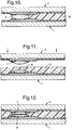
- the mechanical and thermal bond between the chips 2 and the substrate 1 can be improved by applying an electrically-insulating adhesive 16 to the substrate or chips before the chips are brought down onto the substrate, as shown in Figures 9 and 10.
- an electrically-insulating adhesive 16 When the chips 2 are lowered, the insulating adhesive 16 flows between them contacting the upper surface of the substrate and the lower surface of the chip, so as to improve the mechanical and thermal bond. This also reduces the risk of electrical shorts between adjacent bumps.
- a pre-cut film of an electrically-insulating but thermally-conductive thermoplastic material could be applied to the region of the substrate between the bumps.
- an anisotropic (Z-axis) electrically-conductive adhesive is used, as shown in Figures 11 and 12.
- the adhesive 17 is applied as a thin layer over the entire surface of the substrate 1 and the chips 2 are lowered onto the substrate.
- the application of pressure in the region between the bumps 7 and 8 creates contact of the bumps with conductive particles in the adhesive 17.
- the temperature is then raised to cure the adhesive and create an electrical and mechanical bond.
- the present invention enables conventional integrated circuit dice to be treated and modified alter manufacture to provide them with conductive bumps suitable for use in flip-chip assembly.
Landscapes
- Wire Bonding (AREA)
- Internal Circuitry In Semiconductor Integrated Circuit Devices (AREA)
Applications Claiming Priority (2)
| Application Number | Priority Date | Filing Date | Title |
|---|---|---|---|
| GB9415108 | 1994-07-27 | ||
| GB9415108A GB9415108D0 (en) | 1994-07-27 | 1994-07-27 | Electronic assemblies and methods of treatment |
Publications (2)
| Publication Number | Publication Date |
|---|---|
| EP0696055A2 true EP0696055A2 (de) | 1996-02-07 |
| EP0696055A3 EP0696055A3 (de) | 1997-05-02 |
Family
ID=10758929
Family Applications (1)
| Application Number | Title | Priority Date | Filing Date |
|---|---|---|---|
| EP95303811A Withdrawn EP0696055A3 (de) | 1994-07-27 | 1995-06-05 | Elektronischer Zusammenbau und Behandlungsverfahren |
Country Status (3)
| Country | Link |
|---|---|
| EP (1) | EP0696055A3 (de) |
| JP (1) | JPH0855873A (de) |
| GB (2) | GB9415108D0 (de) |
Cited By (2)
| Publication number | Priority date | Publication date | Assignee | Title |
|---|---|---|---|---|
| EP0890989A4 (de) * | 1997-01-24 | 2006-11-02 | Rohm Co Ltd | Halbleitervorrichtung und herstellungsverfahren |
| EP1818987A1 (de) * | 2006-02-10 | 2007-08-15 | ELMOS Semiconductor AG | Halbleiterbauelementanordnung |
Citations (1)
| Publication number | Priority date | Publication date | Assignee | Title |
|---|---|---|---|---|
| EP0372880A2 (de) | 1988-12-05 | 1990-06-13 | Hitachi Chemical Co., Ltd. | Zusammensetzung für eine Schaltungsverbindung, Verbindungsverfahren mit dieser Zusamensetzung und verbundene Struktur für Halbleiterchips |
Family Cites Families (7)
| Publication number | Priority date | Publication date | Assignee | Title |
|---|---|---|---|---|
| EP0265077A3 (de) * | 1986-09-25 | 1989-03-08 | Sheldahl, Inc. | Ein Anisotropisches Klebemittel zum Verbinden elektrischer Bauelemente |
| US4927505A (en) * | 1988-07-05 | 1990-05-22 | Motorola Inc. | Metallization scheme providing adhesion and barrier properties |
| US5074947A (en) * | 1989-12-18 | 1991-12-24 | Epoxy Technology, Inc. | Flip chip technology using electrically conductive polymers and dielectrics |
| US5231053A (en) * | 1990-12-27 | 1993-07-27 | Intel Corporation | Process of forming a tri-layer titanium coating for an aluminum layer of a semiconductor device |
| US5156997A (en) * | 1991-02-11 | 1992-10-20 | Microelectronics And Computer Technology Corporation | Method of making semiconductor bonding bumps using metal cluster ion deposition |
| JPH0661305A (ja) * | 1992-08-11 | 1994-03-04 | Sumitomo Electric Ind Ltd | 半導体装置および半導体素子の実装方法 |
| US5525838A (en) * | 1993-04-08 | 1996-06-11 | Citizen Watch Co., Ltd. | Semiconductor device with flow preventing member |
-
1994
- 1994-07-27 GB GB9415108A patent/GB9415108D0/en active Pending
-
1995
- 1995-06-05 EP EP95303811A patent/EP0696055A3/de not_active Withdrawn
- 1995-06-07 GB GB9511540A patent/GB2292006A/en not_active Withdrawn
- 1995-06-14 JP JP7147334A patent/JPH0855873A/ja active Pending
Patent Citations (1)
| Publication number | Priority date | Publication date | Assignee | Title |
|---|---|---|---|---|
| EP0372880A2 (de) | 1988-12-05 | 1990-06-13 | Hitachi Chemical Co., Ltd. | Zusammensetzung für eine Schaltungsverbindung, Verbindungsverfahren mit dieser Zusamensetzung und verbundene Struktur für Halbleiterchips |
Cited By (2)
| Publication number | Priority date | Publication date | Assignee | Title |
|---|---|---|---|---|
| EP0890989A4 (de) * | 1997-01-24 | 2006-11-02 | Rohm Co Ltd | Halbleitervorrichtung und herstellungsverfahren |
| EP1818987A1 (de) * | 2006-02-10 | 2007-08-15 | ELMOS Semiconductor AG | Halbleiterbauelementanordnung |
Also Published As
| Publication number | Publication date |
|---|---|
| JPH0855873A (ja) | 1996-02-27 |
| GB9511540D0 (en) | 1995-08-02 |
| GB2292006A (en) | 1996-02-07 |
| GB9415108D0 (en) | 1994-09-14 |
| EP0696055A3 (de) | 1997-05-02 |
Similar Documents
| Publication | Publication Date | Title |
|---|---|---|
| JP3554685B2 (ja) | Icチップを支持基板に接合する方法 | |
| US5817541A (en) | Methods of fabricating an HDMI decal chip scale package | |
| US20010003656A1 (en) | Electronic device assembly and a method of connecting electronic devices constituting the same | |
| EP0689240A1 (de) | Lötstruktur und Verfahren zur Herstellung | |
| US5816478A (en) | Fluxless flip-chip bond and a method for making | |
| US20030214007A1 (en) | Wafer-level package with bump and method for manufacturing the same | |
| JPH04234139A (ja) | 半導体チップの基板への直接取付け法 | |
| JPH02246335A (ja) | テープ組立体をボンドさせた半導体装置及びその製造方法 | |
| JPH07231011A (ja) | 導電性接着剤による直接チップ付着 | |
| WO1997018584A1 (en) | Method for forming bump of semiconductor device | |
| KR20050061783A (ko) | 미세 솔더볼 구현을 위한 ubm 및 이를 이용한 플립칩패키지 방법 | |
| JPH07201864A (ja) | 突起電極形成方法 | |
| JP2003508898A (ja) | マイクロビームアセンブリおよび集積回路と基板との内部連結方法 | |
| JP4151136B2 (ja) | 基板および半導体装置とその製造方法 | |
| US20020028535A1 (en) | Circuit, method of adhering an integrated circuit device to a substrate, and method of forming a circuit | |
| JPH10275826A (ja) | 半導体装置およびその製造方法 | |
| JP2910397B2 (ja) | 半田接続方法 | |
| EP0696055A2 (de) | Elektronischer Zusammenbau und Behandlungsverfahren | |
| JPH09148333A (ja) | 半導体装置とその製造方法 | |
| JP2003086620A (ja) | 突起電極を有する半導体装置及びその製造方法 | |
| JP4440494B2 (ja) | 半導体装置の製造方法 | |
| JP3296344B2 (ja) | 半導体装置およびその製造方法 | |
| JP2682496B2 (ja) | フレキシブルフィルム及び半導体装置 | |
| JP2910398B2 (ja) | 半田バンプ形成方法 | |
| JPH02209742A (ja) | テープ自動化ボンディングプロセス用の金/錫共晶ボンディング |
Legal Events
| Date | Code | Title | Description |
|---|---|---|---|
| PUAI | Public reference made under article 153(3) epc to a published international application that has entered the european phase |
Free format text: ORIGINAL CODE: 0009012 |
|
| AK | Designated contracting states |
Kind code of ref document: A2 Designated state(s): DE FR GB IT NL SE |
|
| PUAL | Search report despatched |
Free format text: ORIGINAL CODE: 0009013 |
|
| AK | Designated contracting states |
Kind code of ref document: A3 Designated state(s): DE FR GB IT NL SE |
|
| STAA | Information on the status of an ep patent application or granted ep patent |
Free format text: STATUS: THE APPLICATION IS DEEMED TO BE WITHDRAWN |
|
| 18D | Application deemed to be withdrawn |
Effective date: 19980103 |