EP0702298A2 - Système de traitement de données à commande par microprogramme avec fonction de surveillance de pause - Google Patents
Système de traitement de données à commande par microprogramme avec fonction de surveillance de pause Download PDFInfo
- Publication number
- EP0702298A2 EP0702298A2 EP95114488A EP95114488A EP0702298A2 EP 0702298 A2 EP0702298 A2 EP 0702298A2 EP 95114488 A EP95114488 A EP 95114488A EP 95114488 A EP95114488 A EP 95114488A EP 0702298 A2 EP0702298 A2 EP 0702298A2
- Authority
- EP
- European Patent Office
- Prior art keywords
- signal
- microorder
- receiving
- execution
- input
- Prior art date
- Legal status (The legal status is an assumption and is not a legal conclusion. Google has not performed a legal analysis and makes no representation as to the accuracy of the status listed.)
- Withdrawn
Links
Images


Classifications
-
- G—PHYSICS
- G06—COMPUTING OR CALCULATING; COUNTING
- G06F—ELECTRIC DIGITAL DATA PROCESSING
- G06F11/00—Error detection; Error correction; Monitoring
- G06F11/28—Error detection; Error correction; Monitoring by checking the correct order of processing
Definitions
- the present invention relates to a data processing system, and more specifically to a microprogram controlled data processing system having a function of monitoring a runaway in an instruction execution.
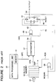
- FIG. 1 there is shown one example of a conventional circuit for monitoring a runaway in an instruction execution in a data processing system, which is disclosed in Japanese Patent Application Laid-open No.JP-A-4-211843.
- a plurality of operation monitoring instructions are previously prepared, and located separately from each other in a stream of a program, so that when the program is executed, the order of execution of operation monitoring instructions and the intervals of execution of operation monitoring instructions are monitored in the stream of the program.
- the system includes a data processing unit 10 coupled to a data bus 12 and an address bus 14, an address decoder 16 connected to the address bus 14 for outputting four address decode signals L1 to L4, and a monitoring circuit 22 connected to receive the four address decode signals L1 to L4, for monitoring a runaway of a program.
- a counter 26 receives and counts a clock CK supplied from an external, for generating a carry signal Co 45, which is supplied to one input of a two-input OR gate 42.
- a shift register 28 is composed of four flipflops (latches) 44.1 to 44.4 cascaded in the form of a ring, and a content of each of the flipflops 44.1 to 44.4 is shifted to a next flipflop in response to an output CL of an inverter 38.
- An output of the four flipflops 44.1 to 44.4 and the four address decode signals L1 to L4 are supplied to four AND gates 30 to 30.4, respectively. More specifically, the AND gate 30.1 receives the output of the flipflop 44.1 and the address decode signal L1, and the AND gate 30.2 receives the output of the flipflop 44.2 and the address decode signal L2. The AND gate 30.3 receives the output of the flipflop 44.3 and the address decode signal L3, and the AND gate 30.4 receives the output of the flipflop 44.4 and the address decode signal L4.
- An output of the AND gates 30 to 30.4 are connected to an OR gate 32.
- the four address decode signals L1 to L4 are supplied to another OR gate 34, and an output 49 of this OR gate 34 is supplied through the inverter 38 to a clock input of the shift register 28.
- an output 47 of the OR gate 32 is inputted to a reset input R of the counter 26, and also supplied through an inverter 35 to an input of an AND gate 40. The other input of this AND gate 40 receives the output 49 of the OR gate 34.
- An output of the AND gate 40 and the carry output 45 of the counter 26 are supplied to an OR gate 42, which in turn has an output supplied as a reset input RS to the data processing unit 10.
- the output of the OR gate 42 is also supplied to reset an initializing circuit 46 for the counter 26 and the shift register 28.
- the data processing unit 10 has previously prepared operation monitor instructions WDI1, WDI2, WDI3 and WDI4, which are previously encoded into a loop included in a program to be executed, by a user, a at suitable intervals and in the order of WDI1, WDI2, WDI3 and WDI4.
- the data processing unit 10 executes the operation monitor instructions WDI1, WDI2, WDI3 and WDI4, respectively, the data processing unit 10 outputs inherent addresses ADR1, ADR2, ADR3 and ADR4 onto the address bus 14, respectively.
- the address decoder 16 activates tile address decode signal L1 when the inherent addresses ADR1 is outputted on the address bus 14, and the address decode signal L2 when the inherent addresses ADR2 is outputted on the address bus 14. Furthermore, the address decoder 16 activates the address decode signal L3 when the inherent addresses ADR3 is outputted on the address bus 14, and the address decode signal L4 when the inherent addresses ADR4 is outputted on the address bus 14.
- the monitor circuit 22 is initialised at the same time as the data processing unit 10 is initialized, in such a manner that the latch 44.1 is set to “1” and the latches 44.2, 44.3 and 44.4 are set to “0”, and the counter 26 is cleared to "0" and the carry signal Co 45 is reset to "0". If the data processing unit starts a processing, the counter 26 is supplied with the clock CK so as to start a count-up.
- the operation monitor instruction WDI1 is executed in the course of a processing, the address ADR1 is outputted to the address bus 14, and therefore, the address decode signal L1 is activated by the address decoder 16. Since the output of the latch 44.1 is "1" in the above mentioned initialized condition, the two-input AND gate 30.1 outputs "1", and therefore, the signal 47 of the OR gate 32 is brought to "1", and the signal 48 is brought to "0". In addition, the output signal 49 of the OR gate 34 is brought to "1".
- the counter 26 In response to the signal 47, the counter 26 is cleared so that the carry signal Co remains at "0". On the other hand, the output of the two-input AND gate 40 is "0", the output signal RS of the OR gate 42 is maintained at "0". Accordingly, the data processing unit (microprocessor) 10 continues to execute the program.
- the inverter 38 receives the signal 49 of "1", and outputs "0" as the clock CL to the shift register 28, so that the latches 44.1, 44.3 and 44.4 are set to "0" and the latch 44.2 is set to "1".
- the address decode signals L2, L3 and L4 are activated, respectively.
- the counter 26 is cleared at activation of each of the address decode signals L2, L3 and L4.
- the shift register 28 becomes the same condition as the initialized condition. Namely, the output of the latch 44.1 is "1" and the output of each of the other latches 44.2, 44.3 and 44.4 is "0". Since the program being executed is a looped condition, the operation monitor instruction WDI1 is executed again, so that the processing is continued.
- a first case is that the data processing unit 10 becomes incapable of responding, so that none of the address decode signals L1, L2, L3 and L4 becomes active.
- the counter 26 is not cleared, and therefore, when the counter 26 has received a predetermined number of clocks at total, the counter 26 becomes overflowed and therefore outputs the carry signal Co of "1". Therefore, the reset signal RS is brought to "1", with the result that the data processing unit 10 and the monitor circuit 22 are initialized, so that the abnormal condition is released.
- a second case is that the order of the execution of the operation monitor instructions WDI1, WDI2, WDI3, and WDI4 is out of order because of abnormality in the processing. This case will be explained about a case in which after initialization, the operation monitor instruction WDI1 is first not executed, but the operation monitor instruction WDI2 is executed.
- the initialized condition is that the latch 44.1 is set to “1” and the latches 44.2, 44.3 and 44.4 are set to “0", and the counter 26 is cleared to “0” and the carry signal Co 45 is reset to “0".
- the operation monitor instruction WDI2 is executed by the data processing unit 10
- the address ADR2 is outputted onto the address bus 14, and the address decode signal L2 is activated to "1".
- the output signal 47 of the OR gate 32 is "0", so that the signal 48 is "1”, and on the other hand, the output signal 49 of the OR gate 34 is brought to "1", with the result that the signal RS is brought to "1".
- the data processing unit 10 and the monitor circuit 22 are initialized, so that the abnormal condition is released.
- the monitor of the runaway is made in connection with the order of the execution of special instructions and the intervals of the execution of special instructions.
- FIG. 2 there is shown another conventional runaway monitor system in a microprogram controlled data processing system, which is disclosed in Japanese Patent Application Laid-open No.JP-A-58-169245.
- This conventional example is configured to compare a microprogram address in an expected order of execution previously prepared in a buffer memory, with an address of a microprogram actually executed.
- a data processing unit 50 is controlled by a microprogram, and is configured so that an address of a microprogram being currently executed is stored in a control memory 51 and is outputted as a signal MPC.
- a buffer memory 52 is formed of a FIFO (first-in first-out) type memory, and is set by the data processing unit 50 with respective addresses of microprograms in the expected order of execution.
- a head data (namely, address) stored in the buffer memory 53 is read out as a signal CPA, and is updated in response to reading clock RDK. If all of the contents of the buffer memory 53 have been read out, the buffer memory 53 generates an empty signal EMP for requesting to set the addresses of succeeding microprograms in the expected order of execution.
- An instruction fetch signal WCSAR 60 is generated at a timing of a microprogram address change, as shown in a timing chart of Figure 13.
- a compare enable signal CEB 60 controls a valid/invalid of a runaway monitor function, and is inactivated to "0" during a period in which no effective data (address) exists in the buffer memory 53.
- a comparator 57 compares the signal MPC with the signal CPA, and outputs a signal 59 which is activated to "1" when coincidence is obtained and to "1" when coincidence is not obtained.
- the compare enable signal CEB 60 and the output signal 59 of the comparator 57 are supplied to an AND gate 61, whose output is connected to an S input of a flipflop 63.
- An inverted output Q ⁇ 65 of the flipflop 63 is also to the AND gate 61.
- the flipflop 63 also has a clock input "ck" connected to receive the instruction fetch signal WCSAR 60 and a non-inverted output Q 64 connected to an R input of the flipflop 63 itself,
- the flipflop 63 also has an asynchronous reset input "res” receiving a reset signal 66.
- the data processing unit 50 checks the result of the monitor, for the purpose of discriminating a normality/abnormality of the operation. If the result of the discrimination shows normality, the data processing unit 50 writes new microprogram addresses in the expected order of execution into the buffer memory 53, so that the runaway monitor is restarted. On the other hand, if the result of the discrimination shows abnormality, the data processing unit 50 goes into an abnormality processing, in which a shift register (not shown) is initialized for example.
- the detection of the runaway is performed at only the timing of writing the microprogram addresses in the expected order of execution into the buffer memory 53. Therefore, if the runaway occurs and the address of the executed microprogram becomes different, the operation cannot go into the abnormality processing, unless the coincidence between the signal MPC and the signal CPA accidentally occurs the number of the valid data stored in the buffer memory 53.
- the first conventional example shown in Figure 1 performs the runaway monitor by paying attention to the order of execution of special instructions and the intervals of execution of the special instructions.
- the second conventional example shown in Figure 2 requires a substantial processing time for detecting abnormality and for releasing the abnormality. Therefore, during a runaway period, the data is broken and the control system becomes out of order. Therefore, it cannot be applied to a field requiring a real time control.
- Another object of the present invention is to provide a microprogram controlled data processing system having a runway monitoring function, capable of detecting the runway in real time with execution of a program, thereby quickly avoiding a break of data and faulty operation of the system, for the purpose of greatly elevating reliability of the system.
- a microprogram controlled data processing system including a microorder generating means for generating a predetermined series of microorders on the basis of an instruction code received, and an execution order detection means for detecting the order of execution of the series of microorders so as to generate an abnormal signal on the basis of the result of the detection.
- the order of execution of the predetermined sequence of microorders is detected, and if abnormal is detected in the order of execution, the abnormal signal is generated to perform a special processing such as a system resetting.
- FIG. 4 there is shown a block diagram of a first embodiment of the microprogram controlled data processing system having a runaway monitoring function in accordance with the present invention.
- the shown data processing system includes a micro ROM 101, an instruction controller 102, a micro decoder 103, a bus controller 104, a runaway controller 105, an OR gate 106 and an inverter 107, which are connected as shown in Figure 4.
- the instruction controller 102 receives an instruction code Q0 supplied internally or externally, a microorder end signal END supplied from the micro decoder 103 and indicating an end of the microorder, and an operation retain request signal OMD also supplied from the micro decoder 103, and outputs a micro address MPC indicative of an execution address of a microprogram. Furthermore, the instruction controller 102 receives a reset signal RES.
- the micro ROM 101 receives the micro address MPC, and outputs microcodes MSTL2, MSTL1 and MSTL0 (where, "MSTL” is an abbreviation of Micro ROM Store Latch).
- the micro decoder 103 receives the microcodes MSTL2, MSTL1 and MSTL0, a status signal LDRDY (where, "LDRDY” is an abbreviation of Load Ready), another status signal STRDY (where, "STRDY” is an abbreviation of Store Ready), and outputs microorder signals DPWR (Date Pointer Write), STRQ (Store Request), STWR (Store Write), LDRQ (Load Request), LDRD (Load Read) and LDRD', and the microorder end signal END.
- the status signal LDRD' is a signal which is supplied to an AND gate together with a Load Ready signal in order to obtain the signal LDRD, and which is an output of an AND gate receiving signals MSTL0, MSTL1B (here, "B" indicates an inverted signal) and MSTL2).
- the bus controller 104 receives the microorder signals DPWR, STRQ, STWR, LDRQ and LDRD, and outputs the state signals LDRDY and STRDY.
- the bus controller 104 also receives the reset signal RES, and is coupled to a data bus DBUS coupled to the instruction controller 102, and another data bus IBUS coupled to to an internal memory (not shown) and an external memory (not shown).
- the runaway detection circuit 105 receives the microorder signals DPWR, STRQ, STWR, LDRQ and LDRD' and the reset signal RES, and outputs a runaway detection signal RESRQ.
- the two-input OR gate 106 has a first input receiving from the inverter 107 an inverted signal of a signal applied to an external terminal RESET B, and a second input receiving the runaway detection signal RESRQ.
- the OR gate 106 generates the reset signal RES.
- the instruction controller 102 generates the microcode address MPS on the basis of a given instruction code Q0 at an instruction start timing. Correspondence between the instruction code Q0 and the micro addresses shown in the table of Figure 5.
- microcode address MPS is determined at the instruction start timing, the microcode address MPS is incremented for each clock C1 until the microorder end signal END is generated. However, during a period in which the retain request signal OMD is at "1", the microcode address MPS is not incremented, so that the current microcode address MPS is maintained. If the microorder end signal END is generated, it is recognized that the current instruction has been completed, and therefore, the processing goes to a next instruction.
- the micro decoder 103 responds to the microcodes MSTL2, MSTL1 and MSTL0 which are supplied from the micro ROM 101 and which are a binary signal indicative of "1" or "0", and generates a group of microorders DPWR, STRQ, STWR, LDRQ, LDRD and END, which function as actual microinstructions. However, during a period in which the status signal LDRDY from the bus controller 104 is at "0", the micro decoder 103 stops generation of the microorder LDRD, and during a period in which the status signal STRDY from the bus controller 104 is at "0", the micro decoder 103 stops generation of the microorder DPWR. In addition, in both situations, the micro decoder 103 activates the retain request signal OMD to "1".
- FIG. 7 there is shown a circuit diagram showing one example of the micro decoder realizing the logic operation shown in the table of Figure 6.
- the micro decoder 103 includes an inverter 121 receiving the signal MSTL2 to output an inverted signal MSTL2B (here, "B" indicates an inverted signal), another inverter 122 receiving the signal MSTL1 to output an inverted signal MSTL1B, and still another inverter 123 receiving the signal MSTL0 to output an inverted signal MSTL0B.
- the micro decoder 103 also includes a further inverter 124 receiving the signal LDRDY to output an inverted signal LDRDYB, and a still further inverter 125 receiving the signal STRDY to output an inverted signal STRDYB.
- the micro decoder 103 further includes a three-input AND gate 110 receiving the signals MSTL0B, MSTL1 and MSTL2 to generate the microorder signal END, a three-input AND gate 111 receiving the signals MSTL0, MSTL1B and MSTL2 to generate the microorder signal LDRD', a three-input AND gate 112 receiving the signals MSTL0B, MSTL1B and MSTL2 to generate the microorder signal LDRQ, a three-input AND gate 113 receiving the signals MSTL0, MSTL1 and MSTL2B to generate the microorder signal STWR, a three-input AND gate 114 receiving the signals MSTL0B, MSTL1 and MSTL2B to generate the microorder signal STRQ, a three-input AND gate 115 receiving the signals MSTL, MSTL1B and MSTL2B to generate the microorder signal DPWR', a two-input AND gate 116 receiving the signals LDRDY and LDRD' to generate the microorder signal LDRD, a two
- the micro ROM 101 receives the micro address MPC and generates the microcodes MSTL2, MSTL1 and MSTL0.
- the micro ROM 101 stores microprograms shown in Figure 8.
- the bus controller 104 can be constituted of a logic circuit having the construction shown in Figure 9
- the bus controller 104 includes a flipflop 180 having a set input S receiving a signal B4, a reset input R receiving the signal STWR, a clock input “ck” receiving the clock C2, an asynchronous set input “set” receiving the reset signal RES and an output Q outputting a signal 263, a flipflop 181 having a set input S receiving the signal B4, a reset input R receiving the signal LDRD, a clock input “ck” receiving the clock C2, an asynchronous reset input “res” receiving the reset signal RES and an output Q outputting a signal 264, a flipflop 182 having a set input S receiving the signal STRQ, a reset input R receiving a signal B1, a clock input "ck” receiving the clock C2, an asynchronous reset input “res” receiving the reset signal RES and an output Q outputting a signal 250, and a flipflop 183 having a set input S receiving the signal LDRQ, a reset input R receiving the signal B1, a clock input "ck” receiving the clock C2, an
- the bus controller 104 also includes a latch 184 having a data input D receiving the signal 250 and a clock input "ck” receiving the clock C1, a latch 185 having a data input D receiving an output of the latch 184 and a clock input “ck” receiving the clock C2, a latch 186 having a data input D receiving the signal 251 and a clock input “ck” receiving the clock C1, and a latch 187 having a data input D receiving an output of the latch 186 and a clock input "ck” receiving the clock C2.
- the bus controller 104 includes an inverter 189 receiving the signal 263 to output a signal 255, another inverter 188 receiving the signal 264 to output a signal 254, a two-input AND gate 190 receiving the signals 252 and 255 to generate a signal 256, a two-input AND gate 191 receiving the signals 253 and 254 to generate a signal 257, a two-input OR gate 192 receiving the signals 256 and 257 to generate a signal 262, and a two-input AND gate 193 receiving the signals 262 and 259,
- the bus controller 104 also includes a latch 196 having a data input D receiving an output of the AND gate 193 and a clock input "ck” receiving the clock C1 so as to generate the above mentioned signal B1, a latch 197 having a data input D receiving the signal B1 and a clock input “ck” receiving the clock C2, a latch 198 having a data input D receiving an output of the latch 197 and a clock input “ck” receiving the clock C1 so as to generate a signal B2, a latch 199 having a data input D receiving the signal B2 and a clock input “ck” receiving the clock C2, a latch 200 having a data input D receiving an output of the latch 199 and a clock input "ck” receiving the clock C1 so as to generate a signal B3, a latch 201 having a data input D receiving the signal B3 and a clock input "ck” receiving the clock C2 so as to generate a signal B3', and a latch 202 having a data input D receiving the signal B3' and a clock input "ck
- the bus controller 104 includes a two-input OR gate 205 receiving a signal 261 and the signal B3' to generate a signal 259, an inverter 194 receiving the signal 262, a two-input AND gate 195 receiving an output of the inverter 194 and the signal 259 to generate a signal 260, a latch 203 having a data input D receiving the signal 260 and a clock input "ck” receiving the clock C1, a latch 204 having a data input D receiving an output of the latch 203 and a clock input "ck” receiving the clock C2 so as to generate the above mentioned signal 261, and a latch 208 having a data input D receiving the signal 255 and a clock input "ck” receiving the clock C1 so as to generate a signal 258.
- the bus controller 104 includes a two-input OR gate 206 receiving the signals B3 and B4, a two-input AND gate 207 receiving an output of the two-input OR gate 206 and the signal 258 so as to generate the signal STRD, a two-input AND gate 209 receiving the signal DPWR and the clock C2, a latch 212 having an input connected to the bus DBUS and a clock input receiving an output of the AND gate 209, a driver 213 receiving an output of the latch 212 and controlled by the signal B2 so as to supply an output to the bus IBUS, a two-input AND gate 210 receiving the signal DPWR and the clock C2, a latch 214 having an input connected to the bus DBUS and a clock input receiving an output of the AND gate 210, a driver 215 receiving an output of the latch 214 and controlled by the signal STRD so as to supply an output to the bus IBUS, a two-input AND gate 211 receiving the signal B4 and the clock C2, a
- the runaway detection circuit 105 which is a featured portion of the present invention, can be constituted of a logic circuit shown in Figure 10.
- the runaway detection circuit 105 includes a flipflop 140 having a set input S receiving the signal DPWR, a reset input R receiving the signal LDRQ, a clock input "ck” receiving the clock C2, an asynchronous reset input “res” receiving the reset signal RES, a latch 146 having a data input D connected to an output Q of the flipflop 140 and a clock input "ck” receiving the clock C1, an inverter 152 receiving an output Q of the latch 146, and a two-input AND gate 158 receiving an output of the inverter 152 and the signal LDRQ.
- the runaway detection circuit 105 also includes a flipflop 141 having a set input S receiving the signal DPWR, a reset input R receiving the signal LDRD', a clock input "ck” receiving the clock C2, an asynchronous reset input “res” receiving the reset signal RES, a latch 147 having a data input D connected to an output Q of the flipflop 141 and a clock input "ck” receiving the clock C1, an inverter 153 receiving an output Q of the latch 147, and a two-input AND gate 159 receiving an output of the inverter 153 and the signal LDRD'.
- the runaway detection circuit 105 includes a flipflop 142 having a set input S receiving the signal LDRD, a reset input R receiving the signal LDRD', a clock input "ck” receiving the clock C2, an asynchronous reset input “res” receiving the reset signal RES, a latch 148 having a data input D connected to an output Q of the flipflop 142 and a clock input "ck” receiving the clock C1, an inverter 154 receiving an output Q of the latch 148, and a two-input AND gate 160 receiving an output of the inverter 154 and the signal LDRD'.
- the runaway detection circuit 105 includes a flipflop 143 having a set input S receiving the signal DPWR, a reset input R receiving the signal STRQ, a clock input "ck” receiving the clock C2, an asynchronous reset input “res” receiving the reset signal RES, a latch 149 having a data input D connected to an output Q of the flipflop 143 and a clock input "ck” receiving the clock C1, an inverter 155 receiving an output Q of the latch 149, and a two-input AND gate 161 receiving an output of the inverter 155 and the signal STRQ.
- the runaway detection circuit 105 also includes a flipflop 144 having a set input S receiving the signal DPWR, a reset input R receiving the signal STWR, a clock input "ck” receiving the clock C2, an asynchronous reset input “res” receiving the reset signal RES, a latch 150 having a data input D connected to an output Q of the flipflop 144 and a clock input "ck” receiving the clock C1, an inverter 156 receiving an output Q of the latch 150 and a two-input AND gate 162 receiving an output of the inverter 156 and the signal STWR.
- the runaway detection circuit 105 includes a flipflop 145 having a set input S receiving the signal STRQ, a reset input R receiving the signal STWR, a clock input "ck” receiving the clock C2, an asynchronous reset input “res” receiving the reset signal RES, a latch 151 having a data input D connected to an output Q of the flipflop 145 and a clock input "ck” receiving the clock C1, an inverter 157 receiving an output Q of the latch 151, a two-input AND gate 163 receiving an output of the inverter 157 and the signal STWR, and a six-input OR gate 164 receiving an output of the AND gates 158, 159, 160, 161, 162 and 163 so as to generate the signal RESRQ.
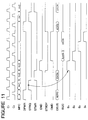
- FIG. 11 A timing chart illustrating a memory WRITE operation is shown in Figure 11.
- the bus controller 104 receives the microorder DPWR of "1", and latches the address on the bus DBUS in the latch 212.
- the micro address MPC is incremented to "n+1", so that the microorder STRQ is brought to "1".
- the output signal 250 of the flipflop 182 shown in Figure 9 is brought to the "1".
- the micro address MPC is incremented to "n+2", so that the microorder STWR is brought to "1".
- the latch 214 shown in Figure 6 latches data on the bus DBUS, and the output signal STRDY of the flipflop 180 is brought to "0". Since the just preceding clock signal 250 has become 1", the signal 252 is brought to "1” and the signal 256 is brought to "1".
- the micro address MPC is incremented to "n+3", so that the microorder END is brought to "1".
- the memory WRITE instruction is completed, so that in response to a next clock, the operation goes into execution of a new instruction.
- the signal B1 is brought to "1".
- the flipflop 182 is reset, so that the signal 250 becomes “0” and the signal STRDY also becomes “0”, with the result that the signal 258 is brought to "1".
- the instruction controller 102 decodes the instruction code Q0.
- the micro address MPC is brought to "n", again.
- the status signal STRDY 0
- the retain request signal OMD is brought "1"
- the signal B2 is brought to "1" so that the address is outputted through the driver 213 to the bus IBUS.
- the retain request signal OMD is brought to "0", so that the microorder DPWR is outputted, and therefore, an operation similar to the above mentioned operation is performed.
- FIG. 12 A timing chart illustrating a memory READ operation is shown in Figure 12.
- the micro address MPC is incremented to "m+1", so that the microorder LDRQ is brought to "1".
- the output signal 251 of the flipflop 183 shown in Figure 9 is brought to the "1".
- the microorder LDRD is not outputted, and the retain request signal OMD is brought to "1".
- the signal 253 is brought to "1” and the signal 257 is brought to "1".
- the microorder LDRD is outputted, and the retain request signal OMD is brought to "0".
- data in the latch 217 is outputted through the driver 216 to the bus DBUS, and the instruction controller 102 then fetches the data on the bus DBUS.
- the flipflop 181 is reset, and the status signal LDRDY is brought to "0".
- the micro address MPC is incremented to "m+3", so that the microorder END is outputted.
- the instruction controller 102 recognizes an end of the instruction,
- the above is an operation of the system in a normal condition.
- the instruction controller 102 outputs the micro address "n+1". Therefore, the microorder STRQ is outputted. Thereafter, the MPC is incremented to "n+2" and then to "n+3", the status changes similarly to the above mentioned data WRITE operation. However, since the microorder DPWR is not generated, the data is written into an indefinite address.
- the instruction controller 102 outputs "n+2" as the micro address MPC. Therefore, the microorder STWR is outputted, and the status signal STRDY is brought to "0".
- the status signal STRDY is set in response to the signal B4 generated from the microorder STRQ, but in this situation, since the microorder STRQ has not been outputted, "Q" continues to be maintained.
- the instruction controller 102 outputs "m+1" as the micro address MPC. Therefore, the microorder LDRQ is outputted. Thereafter, the MPC is incremented to "m+2" and then to "m+3", the status changes similarly to the above mentioned data READ operation. However, since the microorder DPWR is not generated, the data is read from an indefinite address.
- the instruction controller 102 outputs the micro address "n+1". Therefore, the microorder STRQ is outputted.
- the AND gate 161 outputs "1", so that the runaway detection signal RESRQ is brought to "1".
- the reset signal RES is brought to "1” so as to initialize the whole of the system.
- the reset signal RES is brought to "1” at the timing that the microorder STRQ is outputted, it is possible to avoid the writing into the memory.
- the instruction controller 102 outputs "m+1" as the micro address MPC. Therefore, the microorder LDRQ is outputted.
- the output of the inverter 152 is brought to "1", so that the output of the AND gate 158 is brought to "1". Therefore, the runaway detection signal RESRQ is brought to "1".
- the reset signal RES is brought to "1” so as to initialize the whole of the system.
- the reset signal RES is brought to "1" at the timing that the microorder LDRQ is outputted, it is possible to avoid the reading from the memory.
- the first microorder DPWR is applied to the set input of the flipflop 140
- the second microorder LDRQ is applied to the reset input of the flipflop 140
- the Q output of the flipflop 140 is latched in the latch 146 so as to set a flag composed of the latch 146. Accordingly, the flag of the latch 146 indicates "1" if the first microorder DPWR is executed, and "0" if the first microorder DPWR is not executed. Thereafter, the flag maintains that condition, which is transmitted through the inverter 152 to the AND gate 158.
- the order of execution of the microorders DPWR and LDRD' is detected by tile flipflop 141, the latch 147, the inverter 153 and the AND gate 159, and the order of execution of the microorders LDRQ and LDRD' is detected by the flipflop 142, the latch 148, the inverter 154 and the AND gate 160.
- the order of execution of the microorders DPWR and STRQ is detected by the flipflop 143, the latch 149, the inverter 155 and the AND gate 161
- the order of execution of the microorders DPWR and STWR is detected by the flipflop 144, the latch 150, the inverter 156 and the AND gate 162.
- the order of execution of the microorders STRQ and STWR is detected by the flipflop 145, the latch 151, the inverter 157 and the AND gate 163.
- FIG. 13 there is shown a circuit diagram showing another example of a runaway detecting circuit 105, which is the featured portion of the present invention as mentioned hereinbefore.
- the circuit shown in Figure 13 is composed of a reduced number of circuit elements in comparison with the circuit shown in Figure 10..
- the runaway detection circuit shown in Figure 13 is generally designated by Reference Numeral 105A, and includes a flipflop 702 having a set input S receiving tile signal DPWR, a reset input R receiving the signal LDRQ, a clock input "ck” receiving the clock C2, an asynchronous reset input “res” receiving the reset signal RES, a latch 708 having a data input D connected to an output Q of the flipflop 702 and a clock input "ck” receiving the clock C1 so as to output a signal 721, an inverter 712 receiving the signal 721, and a two-input AND gate 716 receiving an output of the inverter 712 and the signal LDRQ.
- the runaway detection circuit 105A also includes a two-input AND gate 706 receiving the signal 721 and the signal LDRQ, a flipflop 703 having a set input S receiving an output of the AND gate 706, a reset input R receiving the signal LDRQ', a clock input "ck” receiving the clock C2, an asynchronous reset input “res” receiving the reset signal RES, a latch 709 having a data input D connected to an output Q of the flipflop 703 and a clock input "ck” receiving the clock C1, an inverter 713 receiving an output of the latch 709, and a two-input AND gate 717 receiving an output of the inverter 713 and the signal LDRQ'.
- the runaway detection circuit 105A further includes a flipflop 704 having a set input S receiving the signal DPWR, a reset input R receiving the signal STRQ, a clock input "ck” receiving the clock C2, an asynchronous reset input “res” receiving the reset signal RES, a latch 710 having a data input D connected to an output Q of the flipflop 704 and a clock input "ck” receiving the clock C1 so as to output a signal 722, an inverter 714 receiving tile signal 722, and a two-input AND gate 718 receiving an output of the inverter 714 and the signal STRQ.
- the runaway detection circuit 105A also includes a two-input AND gate 707 receiving the signal 722 and the signal STRQ, a flipflop 705 having a set input S receiving an output of the AND gate 707, a reset input R receiving the signal STWR, a clock input "ck” receiving the clock C2, an asynchronous reset input “res” receiving the reset signal RES, a latch 711 having a data input D connected to an output Q of the flipflop 705 and a clock input "ck” receiving the clock C1, an inverter 713 receiving an output of the latch 711, a two-input AND gate 719 receiving an output of the inverter 715 and the signal STRQ, and a four-input OR gate 720 receiving an output of the two-input AND gates 716, 717, 718 and 719 so as to generate the runaway detection signal RESRQ.
- a two-input AND gate 707 receiving the signal 722 and the signal STRQ
- a flipflop 705 having a set input S
- the microorder STRQ is outputted.
- the AND gate 718 outputs "1", so that the runaway detection signal RESRQ is brought to "1".
- the reset signal RES is brought to "1" so as to initialize the whole of the system.
- the microorder STRQ is outputted.
- the AND gate 719 outputs "1", so that the runaway detection signal RESRQ is brought to "1".
- the reset signal RES is brought to "1" so as to initialize the whole of the system.
- the microorder LDRQ is outputted.
- the output of the inverter 712 is brought to "1", so that the output of the AND gate 716 is brought to "1". Therefore, the runaway detection signal RESRQ is brought to "1".
- the reset signal RES is brought to "1" so as to initialize the whole of the system.
- the signal LDRD' is outputted.
- the output of the inverter 713 is brought to "1", so that the output of the AND gate 717 is brought to "1". Therefore, the runaway detection signal RESRQ is brought to "1".
- the reset signal RES is brought to "1" so as to initialize the whole of the system.
- This runaway detection circuit 105A is constructed by paying attention to the fact that in response to a given instruction code Q0, a series of microorders DPWR, LDRQ and LDRD' should be generated and executed in the named order, so that the order of execution of the first microorder DPWR and the second microorder LDRQ is detected by the flipflop 702, the latch 708, the inverter 712 and the AND gate 716 (which correspond to the flipflop 140, the latch 146, the inverter 152 and the AND gate 158 shown in Figure 10), and whether or not the third microorder LDRD' is executed following the execution of the second microorder LDRQ is detected by the AND gate 706, the flipflop 703, the latch 709, the inverter 713 and the AND gate 717.
- the flipflop 703 is set to "1" by the output of the AND gates 706.
- the latch 709 is set to "1" when a flag indicating that both of the first microorder DPWR and the second microorder LDRQ have been executed. Therefore, if the execution timing of the third microorder LDRD' and the inverted signal of the flag output of the latch 707 by the inverter 713 are supplied to the AND gate 717, it is possible to discriminate whether or not whether or not the order of execution of the three microorders is correct.
- microorders DPWR and the other microorders STRQ and STWR can be detected.
- the data processing system in accordance with the present invention is characterized in that the order of generation and execution of a series of predetermined microorders generated in response to a given instruction code is monitored so as to detect the runaway. Therefore, it is possible to detect the runaway in real time. Accordingly, it is possible to previously avoid break of data and system abnormality.
Landscapes
- Engineering & Computer Science (AREA)
- Theoretical Computer Science (AREA)
- Quality & Reliability (AREA)
- Physics & Mathematics (AREA)
- General Engineering & Computer Science (AREA)
- General Physics & Mathematics (AREA)
- Debugging And Monitoring (AREA)
Applications Claiming Priority (2)
| Application Number | Priority Date | Filing Date | Title |
|---|---|---|---|
| JP219337/94 | 1994-09-14 | ||
| JP6219337A JP2630271B2 (ja) | 1994-09-14 | 1994-09-14 | 情報処理装置 |
Publications (2)
| Publication Number | Publication Date |
|---|---|
| EP0702298A2 true EP0702298A2 (fr) | 1996-03-20 |
| EP0702298A3 EP0702298A3 (fr) | 1996-09-04 |
Family
ID=16733882
Family Applications (1)
| Application Number | Title | Priority Date | Filing Date |
|---|---|---|---|
| EP95114488A Withdrawn EP0702298A3 (fr) | 1994-09-14 | 1995-09-14 | Système de traitement de données à commande par microprogramme avec fonction de surveillance de pause |
Country Status (3)
| Country | Link |
|---|---|
| US (1) | US5838898A (fr) |
| EP (1) | EP0702298A3 (fr) |
| JP (1) | JP2630271B2 (fr) |
Families Citing this family (5)
| Publication number | Priority date | Publication date | Assignee | Title |
|---|---|---|---|---|
| JPH10214201A (ja) * | 1997-01-29 | 1998-08-11 | Mitsubishi Electric Corp | マイクロコンピュータ |
| JP4008086B2 (ja) * | 1998-02-04 | 2007-11-14 | 沖電気工業株式会社 | データモニタ回路 |
| US6665818B1 (en) * | 2000-04-27 | 2003-12-16 | Hewlett-Packard Development Company, L.P. | Apparatus and method for detecting, diagnosing, and handling deadlock errors |
| KR100444606B1 (ko) * | 2002-07-16 | 2004-08-16 | 주식회사 하이닉스반도체 | 명령 상태 머신 및 그 구동 방법 |
| CN101854259B (zh) * | 2010-06-04 | 2014-03-19 | 中兴通讯股份有限公司 | 一种数据包的计数方法及系统 |
Citations (2)
| Publication number | Priority date | Publication date | Assignee | Title |
|---|---|---|---|---|
| JPS58169245A (ja) | 1982-03-31 | 1983-10-05 | Fujitsu Ltd | マイクロプログラム制御装置 |
| JPH04211843A (ja) | 1990-03-08 | 1992-08-03 | Sony Corp | マイクロプロセッサ装置 |
Family Cites Families (20)
| Publication number | Priority date | Publication date | Assignee | Title |
|---|---|---|---|---|
| JPS4939852B1 (fr) * | 1969-11-19 | 1974-10-29 | ||
| JPS5278334A (en) * | 1975-12-25 | 1977-07-01 | Fujitsu Ltd | Program sequence check system |
| SU613651A1 (ru) * | 1976-12-16 | 1987-03-15 | Предприятие П/Я А-3886 | Запоминающее устройство |
| US4179737A (en) * | 1977-12-23 | 1979-12-18 | Burroughs Corporation | Means and methods for providing greater speed and flexibility of microinstruction sequencing |
| JPS5582359A (en) * | 1978-12-18 | 1980-06-21 | Toshiba Corp | Microprogram test unit |
| US4356546A (en) * | 1980-02-05 | 1982-10-26 | The Bendix Corporation | Fault-tolerant multi-computer system |
| JPS5824951A (ja) * | 1981-08-06 | 1983-02-15 | Fujitsu Ltd | マイクロプログラムのエラ−検出方式 |
| JPS59133610A (ja) * | 1983-01-19 | 1984-08-01 | Omron Tateisi Electronics Co | プログラマブルコントロ−ラ |
| DE3420316C2 (de) * | 1983-05-31 | 1997-01-09 | Canon Kk | Verfahren zur Steuerung eines Kopiergeräts |
| JPS60136810A (ja) * | 1983-12-26 | 1985-07-20 | Fuji Electric Co Ltd | プログラマブルコントロ−ラ |
| JPS61188626A (ja) * | 1985-02-18 | 1986-08-22 | Fujitsu Ltd | マイクロプロセツサ |
| IT1184054B (it) * | 1985-03-25 | 1987-10-22 | Cselt Centro Studi Lab Telecom | Unita di controllo di microprogramma autocollaudante con rilevazione in linea degli errori in tecnologia mos |
| US5263153A (en) * | 1987-01-22 | 1993-11-16 | National Semiconductor Corporation | Monitoring control flow in a microprocessor |
| US4851990A (en) * | 1987-02-09 | 1989-07-25 | Advanced Micro Devices, Inc. | High performance processor interface between a single chip processor and off chip memory means having a dedicated and shared bus structure |
| US5125084A (en) * | 1988-05-26 | 1992-06-23 | Ibm Corporation | Control of pipelined operation in a microcomputer system employing dynamic bus sizing with 80386 processor and 82385 cache controller |
| US5151981A (en) * | 1990-07-13 | 1992-09-29 | International Business Machines Corporation | Instruction sampling instrumentation |
| US5522064A (en) * | 1990-10-01 | 1996-05-28 | International Business Machines Corporation | Data processing apparatus for dynamically setting timings in a dynamic memory system |
| IT1241318B (it) * | 1990-11-19 | 1994-01-10 | Olivetti & Co Spa | Dispositivo di indirizzamento di memoria |
| JPH0540668A (ja) * | 1991-08-06 | 1993-02-19 | Nec Corp | プログラム暴走防止方式 |
| US5530802A (en) * | 1994-06-22 | 1996-06-25 | At&T Corp. | Input sequence reordering method for software failure recovery |
-
1994
- 1994-09-14 JP JP6219337A patent/JP2630271B2/ja not_active Expired - Lifetime
-
1995
- 1995-09-14 US US08/528,054 patent/US5838898A/en not_active Expired - Fee Related
- 1995-09-14 EP EP95114488A patent/EP0702298A3/fr not_active Withdrawn
Patent Citations (2)
| Publication number | Priority date | Publication date | Assignee | Title |
|---|---|---|---|---|
| JPS58169245A (ja) | 1982-03-31 | 1983-10-05 | Fujitsu Ltd | マイクロプログラム制御装置 |
| JPH04211843A (ja) | 1990-03-08 | 1992-08-03 | Sony Corp | マイクロプロセッサ装置 |
Also Published As
| Publication number | Publication date |
|---|---|
| US5838898A (en) | 1998-11-17 |
| EP0702298A3 (fr) | 1996-09-04 |
| JP2630271B2 (ja) | 1997-07-16 |
| JPH0883178A (ja) | 1996-03-26 |
Similar Documents
| Publication | Publication Date | Title |
|---|---|---|
| US3518413A (en) | Apparatus for checking the sequencing of a data processing system | |
| JP3176093B2 (ja) | マイクロプロセッサの割込み制御装置 | |
| US5694617A (en) | System for prioritizing quiesce requests and recovering from a quiescent state in a multiprocessing system with a milli-mode operation | |
| JP3684590B2 (ja) | リセット制御装置及びリセット制御方法 | |
| US4251859A (en) | Data processing system with an enhanced pipeline control | |
| JPH05225067A (ja) | 重要メモリ情報保護装置 | |
| EP0702298A2 (fr) | Système de traitement de données à commande par microprogramme avec fonction de surveillance de pause | |
| EP0270081B1 (fr) | Contrôleur de microprogramme recevant une demande d'interruption pendant l'exécution d'instruction | |
| US4308580A (en) | Data multiprocessing system having protection against lockout of shared data | |
| EP0343668B1 (fr) | Système de commande de normalisation pour des opérations arithmétiques à virgule flottante | |
| US5673391A (en) | Hardware retry trap for millicoded processor | |
| EP0640925B1 (fr) | Système de traitement de données avec interface sériel | |
| JPH07262032A (ja) | 情報処理装置 | |
| US5813039A (en) | Guest execution control system, method and computer process for a virtual machine system | |
| JP3114909B2 (ja) | プログラマブルコントローラの演算エラー処理方法 | |
| JP2569693B2 (ja) | マイクロコンピュータ | |
| JPH07302205A (ja) | マイクロコンピュータ | |
| JPH10312310A (ja) | 中央処理装置の自己診断方法および自己診断機能を備えた中央処理装置 | |
| JP2701799B2 (ja) | マイクロコンピュータ | |
| JPH06208461A (ja) | マイクロプロセッサ | |
| SU1290340A1 (ru) | Микропроцессор | |
| JP2979918B2 (ja) | 割り込み検出回路 | |
| JPH087679B2 (ja) | マイクロプロセッサ | |
| JPS6326732A (ja) | 割込み処理方式 | |
| JPH05143320A (ja) | 浮動小数点演算方式および浮動小数点演算装置 |
Legal Events
| Date | Code | Title | Description |
|---|---|---|---|
| PUAI | Public reference made under article 153(3) epc to a published international application that has entered the european phase |
Free format text: ORIGINAL CODE: 0009012 |
|
| AK | Designated contracting states |
Kind code of ref document: A2 Designated state(s): DE FR GB |
|
| PUAL | Search report despatched |
Free format text: ORIGINAL CODE: 0009013 |
|
| AK | Designated contracting states |
Kind code of ref document: A3 Designated state(s): DE FR GB |
|
| 17P | Request for examination filed |
Effective date: 19961220 |
|
| 17Q | First examination report despatched |
Effective date: 20000128 |
|
| GRAG | Despatch of communication of intention to grant |
Free format text: ORIGINAL CODE: EPIDOS AGRA |
|
| GRAG | Despatch of communication of intention to grant |
Free format text: ORIGINAL CODE: EPIDOS AGRA |
|
| GRAH | Despatch of communication of intention to grant a patent |
Free format text: ORIGINAL CODE: EPIDOS IGRA |
|
| GRAH | Despatch of communication of intention to grant a patent |
Free format text: ORIGINAL CODE: EPIDOS IGRA |
|
| STAA | Information on the status of an ep patent application or granted ep patent |
Free format text: STATUS: THE APPLICATION HAS BEEN WITHDRAWN |
|
| 18W | Application withdrawn |
Withdrawal date: 20010830 |