EP0710982B1 - Personalisierte Fläche eines Leiterrahmes geformt oder halb-geätzt zur Reduzierung mechanischer Beanspruchung an den Chipkanten - Google Patents
Personalisierte Fläche eines Leiterrahmes geformt oder halb-geätzt zur Reduzierung mechanischer Beanspruchung an den Chipkanten Download PDFInfo
- Publication number
- EP0710982B1 EP0710982B1 EP95480162A EP95480162A EP0710982B1 EP 0710982 B1 EP0710982 B1 EP 0710982B1 EP 95480162 A EP95480162 A EP 95480162A EP 95480162 A EP95480162 A EP 95480162A EP 0710982 B1 EP0710982 B1 EP 0710982B1
- Authority
- EP
- European Patent Office
- Prior art keywords
- lead
- chip
- fingers
- loc
- adhesive layer
- Prior art date
- Legal status (The legal status is an assumption and is not a legal conclusion. Google has not performed a legal analysis and makes no representation as to the accuracy of the status listed.)
- Expired - Lifetime
Links
Images


Classifications
-
- H—ELECTRICITY
- H10—SEMICONDUCTOR DEVICES; ELECTRIC SOLID-STATE DEVICES NOT OTHERWISE PROVIDED FOR
- H10W—GENERIC PACKAGES, INTERCONNECTIONS, CONNECTORS OR OTHER CONSTRUCTIONAL DETAILS OF DEVICES COVERED BY CLASS H10
- H10W70/00—Package substrates; Interposers; Redistribution layers [RDL]
- H10W70/40—Leadframes
-
- H—ELECTRICITY
- H10—SEMICONDUCTOR DEVICES; ELECTRIC SOLID-STATE DEVICES NOT OTHERWISE PROVIDED FOR
- H10W—GENERIC PACKAGES, INTERCONNECTIONS, CONNECTORS OR OTHER CONSTRUCTIONAL DETAILS OF DEVICES COVERED BY CLASS H10
- H10W42/00—Arrangements for protection of devices
-
- H—ELECTRICITY
- H10—SEMICONDUCTOR DEVICES; ELECTRIC SOLID-STATE DEVICES NOT OTHERWISE PROVIDED FOR
- H10W—GENERIC PACKAGES, INTERCONNECTIONS, CONNECTORS OR OTHER CONSTRUCTIONAL DETAILS OF DEVICES COVERED BY CLASS H10
- H10W70/00—Package substrates; Interposers; Redistribution layers [RDL]
- H10W70/40—Leadframes
- H10W70/411—Chip-supporting parts, e.g. die pads
- H10W70/415—Leadframe inner leads serving as die pads
-
- H—ELECTRICITY
- H10—SEMICONDUCTOR DEVICES; ELECTRIC SOLID-STATE DEVICES NOT OTHERWISE PROVIDED FOR
- H10W—GENERIC PACKAGES, INTERCONNECTIONS, CONNECTORS OR OTHER CONSTRUCTIONAL DETAILS OF DEVICES COVERED BY CLASS H10
- H10W72/00—Interconnections or connectors in packages
- H10W72/50—Bond wires
- H10W72/531—Shapes of wire connectors
- H10W72/536—Shapes of wire connectors the connected ends being ball-shaped
-
- H—ELECTRICITY
- H10—SEMICONDUCTOR DEVICES; ELECTRIC SOLID-STATE DEVICES NOT OTHERWISE PROVIDED FOR
- H10W—GENERIC PACKAGES, INTERCONNECTIONS, CONNECTORS OR OTHER CONSTRUCTIONAL DETAILS OF DEVICES COVERED BY CLASS H10
- H10W72/00—Interconnections or connectors in packages
- H10W72/50—Bond wires
- H10W72/531—Shapes of wire connectors
- H10W72/5363—Shapes of wire connectors the connected ends being wedge-shaped
-
- H—ELECTRICITY
- H10—SEMICONDUCTOR DEVICES; ELECTRIC SOLID-STATE DEVICES NOT OTHERWISE PROVIDED FOR
- H10W—GENERIC PACKAGES, INTERCONNECTIONS, CONNECTORS OR OTHER CONSTRUCTIONAL DETAILS OF DEVICES COVERED BY CLASS H10
- H10W72/00—Interconnections or connectors in packages
- H10W72/851—Dispositions of multiple connectors or interconnections
- H10W72/853—On the same surface
- H10W72/865—Die-attach connectors and bond wires
-
- H—ELECTRICITY
- H10—SEMICONDUCTOR DEVICES; ELECTRIC SOLID-STATE DEVICES NOT OTHERWISE PROVIDED FOR
- H10W—GENERIC PACKAGES, INTERCONNECTIONS, CONNECTORS OR OTHER CONSTRUCTIONAL DETAILS OF DEVICES COVERED BY CLASS H10
- H10W90/00—Package configurations
- H10W90/701—Package configurations characterised by the relative positions of pads or connectors relative to package parts
- H10W90/731—Package configurations characterised by the relative positions of pads or connectors relative to package parts of die-attach connectors
- H10W90/736—Package configurations characterised by the relative positions of pads or connectors relative to package parts of die-attach connectors between a chip and a stacked lead frame, conducting package substrate or heat sink
-
- H—ELECTRICITY
- H10—SEMICONDUCTOR DEVICES; ELECTRIC SOLID-STATE DEVICES NOT OTHERWISE PROVIDED FOR
- H10W—GENERIC PACKAGES, INTERCONNECTIONS, CONNECTORS OR OTHER CONSTRUCTIONAL DETAILS OF DEVICES COVERED BY CLASS H10
- H10W90/00—Package configurations
- H10W90/701—Package configurations characterised by the relative positions of pads or connectors relative to package parts
- H10W90/751—Package configurations characterised by the relative positions of pads or connectors relative to package parts of bond wires
- H10W90/756—Package configurations characterised by the relative positions of pads or connectors relative to package parts of bond wires between a chip and a stacked lead frame, conducting package substrate or heat sink
-
- Y—GENERAL TAGGING OF NEW TECHNOLOGICAL DEVELOPMENTS; GENERAL TAGGING OF CROSS-SECTIONAL TECHNOLOGIES SPANNING OVER SEVERAL SECTIONS OF THE IPC; TECHNICAL SUBJECTS COVERED BY FORMER USPC CROSS-REFERENCE ART COLLECTIONS [XRACs] AND DIGESTS
- Y10—TECHNICAL SUBJECTS COVERED BY FORMER USPC
- Y10T—TECHNICAL SUBJECTS COVERED BY FORMER US CLASSIFICATION
- Y10T29/00—Metal working
- Y10T29/49—Method of mechanical manufacture
- Y10T29/49002—Electrical device making
- Y10T29/49117—Conductor or circuit manufacturing
- Y10T29/49121—Beam lead frame or beam lead device
Definitions
- the present invention generally relates to lead-on-chip (LOC) packaging, also known as A-wire packaging, for semiconductor devices and, more particularly, to a planar leadframe having a notched lead-finger configuration for reducing mechanical stress at the chip edge.
- LOC lead-on-chip
- Chips packaged in this manner are sometimes referred to as spiders since the lead-fingers resemble spider legs emanating from around a chip body.
- the contacts 16 are formed by partially etching the lead-fingers 14 near the tip to leave a bump of conductive material.
- the lead-fingers are bonded directly to the chip by applying pressure and forcing the lead-fingers into the active chip face as shown by arrow 18.
- the raised contacts 16 ensures that the whole finger is not smashed into the chip face when bonding pressure is applied.
- U.S. Patent 4,924,292 to Kaufman shows a similar direct bonding technique except that instead of an etched bump, the finger is crimped near the tip to arch the length portion of the finger away from the chip surface.
- FIG. 2 shows a leadframe package having lead-fingers 30 which are spaced around the periphery of the chip 32.
- lead-fingers 30 which are spaced around the periphery of the chip 32.
- each finger is wirebonded to the chip. This makes it possible to connect many more leads to the chip than was previously possible with direct bonding.
- Wirebonds 34 electrically connect lead contacts 38 to chip contacts 36 on the periphery of the chip 32.
- the wirebonds inherently possess high impedance which, when compounded by their length, present undesirable electrical characteristics and signal delays.
- almost no heat dissipation is provided for the chip and the peripherally distributed contacts provide multiple entry points for contamination.
- U.S. Patent 4,864,245 to Pashby et al. shows a Lead-On-Chip (LOC) semiconductor package, designed to eliminate the aforementioned problems.
- LOC Lead-On-Chip
- all electrical chip connections route through vias 40 extending in lines down the center of the active chip face 42.
- Flat lead-fingers 44 are secured on either side of the chip with an insulating adhesive strip 45. Rows of lead-fingers run parallel to each other and arch directly over the active face of the chip terminating just short of the center at the adhesive strip 45. Since all connections are made at the center of the chip, shorter wirebonds 46 which are substantially uniform in length may be used.
- LOC packages of this type having center line connections greatly reduce the signal delays and timing variances associated with the periphery connections of the prior art and generally improve the electrical characteristics of the package. Furthermore, the lead-fingers aid heat dissipation to some degree since they tend to carry heat away from the chip at the adhesive strip 45.
- leadframes are normally made of a material which has a low coefficient of thermal expansion close to that of silicon, such as, for example, copper or nickel-iron alloys.
- silicon such as, for example, copper or nickel-iron alloys.
- the coefficients are closely matched, high stresses are still experienced in LOC packages.
- Even small variations in thermal expansions tend to aggregate at the chip edge and cause cracking or other damage to the active chip face leading premature chip failure or spurious chip operation.
- non-planar, downset leadframes are not stackable since leadframes near the bottom may collapse under the weight of the leadframes on top. Furthermore, downset leadframes only offer minimal heat dissipation since the lead-fingers only contact a small surface of the chip face.
- LOC lead-on-chip
- a planar leadframe package for a semiconductor chip has opposite rows of flat lead-fingers which ingress over a large surface area of the active face of the chip and cantilever off the peripheral edge of the chip at one end.
- the lead fingers are attached in mechanical and thermal contact with active face of the chip by double-sided adhesive tape.
- Electrical connections between the lead-fingers and the chip are made by wirebond connections at a center connection strip running down the center of the chip. Heat generated by the chip is effectively conducted away from the chip and dissipated from the leadframe package by the lead-fingers.
- Each of the lead-fingers has a notched portion positioned directly over the chip edge. The notch prevents differences in thermal expansion rates between the chip, adhesive tape, and lead-finger from stressing the vulnerable chip edge. Additionally, since corrosion typically follows a lead path, the notch provides an increasing path length to prevent corrosive ingress over the chip face.
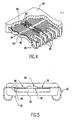
- the semiconductor package incudes encapsulant (50) for encasing a semiconductor chip 52.
- the chip 52 includes an active face 54 covered by a double sided adhesive layer or tape 55.
- a center connection strip 58 extends down the center of the active chip face.
- a portion of the adhesive layer 55 is removed to provide access to chip contact pads (not shown).
- Wirebonds 63 electrically connect a plurality of lead-fingers 60 to chip contact pads (not shown).
- the lead-fingers 60 are cantilevered over a peripheral edge of the chip 52 and are routed over the double sided adhesive layer 55 in paths personalized to cover a predetermined portion of the surface area for a particular chip 52.
- the center connection strip 58 runs down an axis of the chip 52 and the lead-fingers 60 are cantilevered in parallel rows from opposite sides of the chip 52 parallel to the center connection strip 58.
- the lead-fingers 60 are routed in parallel paths with 90° bends over the double sided adhesive layer 55 and terminate perpendicular to the center connection strip 58.
- the double sided adhesive layer 55 securely adheres the lead-fingers 60 in mechanical and thermal contact over a large portion of the of the active face of the chip 54.
- the double sided adhesive layer 55 may either be applied to the lead-fingers 60 and then to the chip face 54 or vice-versa.
- the lead-fingers 60 have a wide portion 62 which extends out of the package 50 and tapers to a thinner width over the chip 52.
- the personalized routing of the lead-fingers 60 ensures that a large surface area of the active chip face 54 is in mechanical and thermal contact with the lead-fingers 60. This reduces the risk of corrosion causing contaminates contacting the chip face is reduced. Additionally, the comprehensive surface area coverage of the lead-fingers 60 over the active face provide an effective vehicle for dissipating substantial quantities of heat which are generated by the chip 52.
- the lead-fingers 60 and the chip 52 are coined or half-etched to create a notch 66 over the chip edge.
- the notch eliminates shear-stress caused by the lead frame at the chip edge and thereby increases chip life and reliability.
- the notch is shown as being square; however, the notch may be of any shape, such as, for example, rectangular, semi-circular, triangular, or a random shape. Additionally, since corrosion typically follows a lead path, the notch provides an increased path length to prevent corrosive ingress over the chip face.
- Figure 5 shows a cross sectional view of a semiconductor package having a notched lead-finger similar to the package shown in Figure 4 except that the lead-fingers 60 are shown as being straight and extending across the active chip face 54, over adhesive layer 55.
- the notched portion of the lead-finger 66 is shown positioned over the chip edge 52 to alleviate mechanical shear-stress at the edge and corrosive ingress.
Landscapes
- Lead Frames For Integrated Circuits (AREA)
- Structures Or Materials For Encapsulating Or Coating Semiconductor Devices Or Solid State Devices (AREA)
Claims (15)
- Lead-on-Chip-Halbleiterpaket (LOC-Halbleiterpaket), das Folgendes umfasst:einen Halbleiterchip (52) mit einer aktiven Fläche (54), die an einer Außenkante endet;eine Klebschicht (55), die mindestens einen Teil der besagten aktiven Fläche (54) des besagten Halbleiterchips (52) bedeckt;eine Vielzahl Kontaktfinger (60) mit einem ersten Teil, der sich flach über die besagte aktive Fläche (54) des besagten Halbleiterchips (52) in Kontakt mit der besagten Klebschicht (55) erstreckt, und einem zweiten Teil, der sich über die besagte Außenkante hinaus erstreckt, wobei jeder der besagten Vielzahl von Kontaktfingern (60) mit einer Aussparung (66) versehen ist, die ausschließlich direkt über der besagten Außenkante verläuft; undeine Umkapselung (50), in der der besagte Halbleiterchip (52) eingeschlossen ist, wobei die besagten Kontaktfinger (60) aus der besagten Umkapselung (50) heraus verlaufen.
- Lead-on-Chip-Halbleiterpaket (LOC-Halbleiterpaket) entsprechend Anspruch 1, gekennzeichnet dadurch, dass es darüber hinaus Folgendes umfasst:einen mittleren Verbindungsstreifen (58), der über die besagte aktive Fläche (54) hinweg verläuft, wobei der besagte erste Teil der besagten Kontaktfinger (60) vor dem besagten mittleren Verbindungsstreifen (58) endet; undDrahtverbindungen (63), durch die eine elektrische Verbindung zwischen den besagten Kontaktfingern (60) und dem besagten Halbleiterchip (52) an dem besagten mittleren Verbindungsstreifen (58) hergestellt wird.
- Lead-on-Chip-Halbleiterpaket (LOC-Halbleiterpaket) entsprechend Anspruch 1, gekennzeichnet dadurch, dass die besagte Klebschicht (55) als doppelseitiges Klebeband ausgeführt ist.
- Lead-on-Chip-Halbleiterpaket (LOC-Halbleiterpaket) entsprechend Anspruch 1, gekennzeichnet dadurch, dass der besagte erste Teil der besagten Vielzahl von Kontaktfingern (60) parallel über der besagten Klebschicht (55) verläuft, wodurch ein vorbestimmter Teil der besagten aktiven Fläche (54) abgedeckt wird.
- Lead-on-Chip-Halbleiterpaket (LOC-Halbleiterpaket) entsprechend Anspruch 4, gekennzeichnet dadurch, dass der besagte erste Teil der besagten Vielzahl von Kontaktfingern (60), der über der besagten Klebschicht (55) verläuft, um 90E abgewinkelt ist.
- Lead-on-Chip-Halbleiterpaket (LOC-Halbleiterpaket) entsprechend Anspruch 1, gekennzeichnet dadurch, dass der besagte erste Teil der besagten Vielzahl von Kontaktfingern (60) schmaler als der besagte zweite Teil ist.
- Verfahren zur Herstellung eines Planar-Lead-on-Chip-Halbleiterpakets (LOC-Halbleiterpakets) mit einer Vielzahl von Kontaktfingern (60), das folgende Schritte umfasst:Aufbringen einer Klebschicht (55) auf mindestens einen Teil einer aktiven Fläche (54) eines Halbleiterchips (52), wobei die besagte Klebschicht (55) an einer Außenkante des besagten Halbleiterchips (52) endet;Ausformen einer Aussparung (66) in jedem der besagten Vielzahl von Kontaktfingern (60);Anbringen der besagten Vielzahl von Kontaktfingern (60) an der besagten Klebschicht (55), wobei die besagte Aussparung (66) in jedem der besagten Vielzahl von Kontaktfingern (60) ausschließlich direkt über der besagten Außenkante verläuft;Herstellen einer Drahtverbindung zwischen der besagten Vielzahl von Kontaktfingern (60) und dem besagten Halbleiterchip (52) an einem Verbindungsstreifen (58), der mittig über die besagte aktive Chipfläche (54) verläuft; undEinschließen des besagten Halbleiterchips (52) und der besagten Vielzahl von Kontaktfingern (60) in einer Umkapselung (50), wobei ein Teil der besagten Kontaktfinger (60) aus der besagten Umkapselung (50) herausragt.
- Verfahren zur Herstellung eines Lead-on-Chip-Halbleiterpakets (LOC-Halbleiterpakets) entsprechend Anspruch 7, gekennzeichnet dadurch, dass es sich bei der besagten Klebschicht (55) um doppelseitiges Band handelt.
- Verfahren zur Herstellung eines Lead-on-Chip-Halbleiterpakets (LOC-Halbleiterpakets) entsprechend Anspruch 7, gekennzeichnet dadurch, dass der besagte Schritt zur Ausformung einer Aussparung (66) in jedem der besagten Vielzahl von Kontaktfingern (60) durch Halb-Ätzung ausgeführt wird.
- Verfahren zur Herstellung eines Lead-on-Chip-Halbleiterpakets (LOC-Halbleiterpakets) entsprechend Anspruch 7, gekennzeichnet dadurch, dass der besagte Schritt zur Ausformung einer Aussparung (66) in jedem der besagten Vielzahl von Kontaktfingern (60) durch Formen ausgeführt wird.
- Verfahren zur Herstellung eines Lead-on-Chip-Halbleiterpakets (LOC-Halbleiterpakets) entsprechend Anspruch 7, gekennzeichnet dadurch, dass es außerdem den Schritt des parallelen Führens der besagten Vielzahl von Kontaktfingern (60) über die besagte Klebschicht (55) umfasst, so dass ein vorbestimmter Teil der besagten aktiven Fläche (54) abgedeckt wird.
- Lead-on-Chip-Halbleiter-Leiterrahmen-Paket (LOC-Halbleiter-Leiterrahmen-Paket), das Folgendes umfasst:eine Klebschicht (55), die mindestens einen Teil einer aktiven Fläche (54) eines Halbleiterchips (52) abdeckt;eine Vielzahl Kontaktfinger (60), die flach über der besagten Klebschicht (55) verlaufen, wobei mindestens einer aus der besagten Vielzahl von Kontaktfingern (60) mit einer Aussparung (66) versehen ist, die so positioniert ist, dass sie ausschließlich über die besagte Außenkante des besagten Halbleiterchips (52) passt.
- Verfahren zur Herstellung eines Lead-on-Chip-Leiterrahmens (LOC-Leiterrahmens) mit einer Vielzahl von Kontaktfingern, das folgende Schritte umfasst:Verfügbarmachen einer Vielzahl von Kontaktfingern (60) ;Ausformen einer Aussparung (66) an einer Unterseite von mindestens einem aus der besagten Vielzahl von Kontaktfingern (60), wobei die besagte Aussparung (66) so positioniert ist, dass sie ausschließlich über die besagte Außenkante eines besagten Halbleiterchips (52) passt; undAnbringen von Klebeband an der besagten Unterseite der besagten Vielzahl von Kontaktfingern (60), so dass die Kontaktfinger (60) sicher in einer festen Konfiguration angebracht sind.
- Verfahren zur Herstellung eines Lead-on-Chip-Leiterrahmens (LOC-Leiterrahmens) entsprechend Anspruch 13, gekennzeichnet dadurch, dass der besagte Schritt zur Ausformung einer Aussparung (66) an einer Unterseite von mindestens einem aus der besagten Vielzahl von Kontaktfingern (60) durch Halb-Ätzung ausgeführt wird.
- Verfahren zur Herstellung eines Lead-on-Chip-Leiterrahmens (LOC-Leiterrahmens) entsprechend Anspruch 13, gekennzeichnet dadurch, dass der besagte Schritt zur Ausformung einer Aussparung (66) an einer Unterseite von. mindestens einem aus der besagten Vielzahl von Kontaktfingern (60) durch Formen ausgeführt wird.
Applications Claiming Priority (2)
| Application Number | Priority Date | Filing Date | Title |
|---|---|---|---|
| US08/334,478 US5545921A (en) | 1994-11-04 | 1994-11-04 | Personalized area leadframe coining or half etching for reduced mechanical stress at device edge |
| US334478 | 1999-06-16 |
Publications (3)
| Publication Number | Publication Date |
|---|---|
| EP0710982A2 EP0710982A2 (de) | 1996-05-08 |
| EP0710982A3 EP0710982A3 (de) | 1996-05-15 |
| EP0710982B1 true EP0710982B1 (de) | 2002-08-14 |
Family
ID=23307395
Family Applications (1)
| Application Number | Title | Priority Date | Filing Date |
|---|---|---|---|
| EP95480162A Expired - Lifetime EP0710982B1 (de) | 1994-11-04 | 1995-11-02 | Personalisierte Fläche eines Leiterrahmes geformt oder halb-geätzt zur Reduzierung mechanischer Beanspruchung an den Chipkanten |
Country Status (7)
| Country | Link |
|---|---|
| US (2) | US5545921A (de) |
| EP (1) | EP0710982B1 (de) |
| JP (1) | JP2923236B2 (de) |
| KR (1) | KR0174341B1 (de) |
| AT (1) | ATE222402T1 (de) |
| DE (1) | DE69527761T2 (de) |
| TW (1) | TW303509B (de) |
Families Citing this family (20)
| Publication number | Priority date | Publication date | Assignee | Title |
|---|---|---|---|---|
| JP3309686B2 (ja) * | 1995-03-17 | 2002-07-29 | セイコーエプソン株式会社 | 樹脂封止型半導体装置及びその製造方法 |
| TW314650B (de) * | 1995-06-21 | 1997-09-01 | Oki Electric Ind Co Ltd | |
| US5811875A (en) * | 1995-06-29 | 1998-09-22 | Samsung Electronics Co., Ltd. | Lead frames including extended tie-bars, and semiconductor chip packages using same |
| US6277225B1 (en) | 1996-03-13 | 2001-08-21 | Micron Technology, Inc. | Stress reduction feature for LOC lead frame |
| JPH09283545A (ja) * | 1996-04-10 | 1997-10-31 | Oki Electric Ind Co Ltd | 樹脂封止型半導体装置及びその製造方法 |
| KR100216064B1 (ko) * | 1996-10-04 | 1999-08-16 | 윤종용 | 반도체 칩 패키지 |
| KR100227149B1 (ko) * | 1997-04-15 | 1999-10-15 | 김영환 | 반도체 패키지 |
| US5923081A (en) | 1997-05-15 | 1999-07-13 | Micron Technology, Inc. | Compression layer on the leadframe to reduce stress defects |
| US6159764A (en) * | 1997-07-02 | 2000-12-12 | Micron Technology, Inc. | Varied-thickness heat sink for integrated circuit (IC) packages and method of fabricating IC packages |
| JP2891692B1 (ja) | 1997-08-25 | 1999-05-17 | 株式会社日立製作所 | 半導体装置 |
| KR100401536B1 (ko) * | 1997-12-31 | 2004-01-24 | 주식회사 하이닉스반도체 | 센터 패드형 반도체 칩을 퍼리퍼럴 패드형 반도체 칩으로 변경하는 방법 |
| US6256200B1 (en) * | 1999-05-27 | 2001-07-03 | Allen K. Lam | Symmetrical package for semiconductor die |
| US6512304B2 (en) * | 2000-04-26 | 2003-01-28 | International Rectifier Corporation | Nickel-iron expansion contact for semiconductor die |
| US9041202B2 (en) | 2008-05-16 | 2015-05-26 | Semiconductor Energy Laboratory Co., Ltd. | Semiconductor device and manufacturing method of the same |
| EP2688093B1 (de) | 2012-07-19 | 2018-07-18 | Technische Universität Ilmenau | Verfahren und Vorrichtung zur Selbstmontage mittels eines Fluids von Komponenten auf einem Substrat |
| WO2014020470A1 (en) * | 2012-07-30 | 2014-02-06 | Koninklijke Philips N.V. | Strengthened led package and method therefor |
| US10211172B2 (en) * | 2014-03-13 | 2019-02-19 | Maxim Integrated Products, Inc. | Wafer-based electronic component packaging |
| US9892860B2 (en) | 2014-11-24 | 2018-02-13 | Avx Corporation | Capacitor with coined lead frame |
| US10242935B2 (en) | 2017-08-31 | 2019-03-26 | Nxp Usa, Inc. | Packaged semiconductor device and method for forming |
| CN108010890A (zh) * | 2017-12-29 | 2018-05-08 | 苏州晶方半导体科技股份有限公司 | 芯片封装结构和方法 |
Citations (1)
| Publication number | Priority date | Publication date | Assignee | Title |
|---|---|---|---|---|
| US5068712A (en) * | 1988-09-20 | 1991-11-26 | Hitachi, Ltd. | Semiconductor device |
Family Cites Families (21)
| Publication number | Priority date | Publication date | Assignee | Title |
|---|---|---|---|---|
| US4210926A (en) * | 1977-12-07 | 1980-07-01 | Siemens Aktiengesellschaft | Intermediate member for mounting and contacting a semiconductor body |
| US4209355A (en) * | 1978-07-26 | 1980-06-24 | National Semiconductor Corporation | Manufacture of bumped composite tape for automatic gang bonding of semiconductor devices |
| JPS57133655A (en) * | 1981-02-10 | 1982-08-18 | Pioneer Electronic Corp | Lead frame |
| US4722060A (en) * | 1984-03-22 | 1988-01-26 | Thomson Components-Mostek Corporation | Integrated-circuit leadframe adapted for a simultaneous bonding operation |
| US4754912A (en) * | 1984-04-05 | 1988-07-05 | National Semiconductor Corporation | Controlled collapse thermocompression gang bonding |
| US4862245A (en) * | 1985-04-18 | 1989-08-29 | International Business Machines Corporation | Package semiconductor chip |
| US4810620A (en) * | 1985-06-26 | 1989-03-07 | National Semiconductor Corporation | Nickel plated tape |
| US4803540A (en) * | 1986-11-24 | 1989-02-07 | American Telephone And Telegraph Co., At&T Bell Labs | Semiconductor integrated circuit packages |
| US5184208A (en) * | 1987-06-30 | 1993-02-02 | Hitachi, Ltd. | Semiconductor device |
| US4924292A (en) * | 1988-04-12 | 1990-05-08 | Kaufman Lance R | Direct bond circuit assembly with crimped lead frame |
| JPH0286155A (ja) * | 1988-09-22 | 1990-03-27 | Hitachi Ltd | リードフレーム |
| US4864245A (en) | 1988-11-22 | 1989-09-05 | Kasha Amplifiers | Modification unit for an amplifier |
| US5227661A (en) * | 1990-09-24 | 1993-07-13 | Texas Instruments Incorporated | Integrated circuit device having an aminopropyltriethoxysilane coating |
| US5177032A (en) * | 1990-10-24 | 1993-01-05 | Micron Technology, Inc. | Method for attaching a semiconductor die to a leadframe using a thermoplastic covered carrier tape |
| US5229329A (en) * | 1991-02-28 | 1993-07-20 | Texas Instruments, Incorporated | Method of manufacturing insulated lead frame for integrated circuits |
| US5403785A (en) * | 1991-03-03 | 1995-04-04 | Matsushita Electric Works, Ltd. | Process of fabrication IC chip package from an IC chip carrier substrate and a leadframe and the IC chip package fabricated thereby |
| JPH05109928A (ja) * | 1991-10-14 | 1993-04-30 | Mitsubishi Electric Corp | 樹脂封止型半導体装置用リードフレームおよびこれを用いた樹脂封止型半導体装置 |
| JP2509422B2 (ja) * | 1991-10-30 | 1996-06-19 | 三菱電機株式会社 | 半導体装置及びその製造方法 |
| JPH05136312A (ja) * | 1991-11-15 | 1993-06-01 | Sony Corp | 半導体装置 |
| JPH0621321A (ja) * | 1992-01-29 | 1994-01-28 | Texas Instr Inc <Ti> | 電気部品実装用支持体付きの集積回路装置 |
| US5457071A (en) * | 1993-09-03 | 1995-10-10 | International Business Machine Corp. | Stackable vertical thin package/plastic molded lead-on-chip memory cube |
-
1994
- 1994-11-04 US US08/334,478 patent/US5545921A/en not_active Expired - Lifetime
-
1995
- 1995-06-02 US US08/458,848 patent/US5576246A/en not_active Expired - Lifetime
- 1995-10-26 JP JP7279103A patent/JP2923236B2/ja not_active Expired - Fee Related
- 1995-11-02 EP EP95480162A patent/EP0710982B1/de not_active Expired - Lifetime
- 1995-11-02 AT AT95480162T patent/ATE222402T1/de not_active IP Right Cessation
- 1995-11-02 DE DE69527761T patent/DE69527761T2/de not_active Expired - Lifetime
- 1995-11-03 KR KR1019950039572A patent/KR0174341B1/ko not_active Expired - Fee Related
- 1995-11-29 TW TW084112699A patent/TW303509B/zh active
Patent Citations (1)
| Publication number | Priority date | Publication date | Assignee | Title |
|---|---|---|---|---|
| US5068712A (en) * | 1988-09-20 | 1991-11-26 | Hitachi, Ltd. | Semiconductor device |
Also Published As
| Publication number | Publication date |
|---|---|
| JP2923236B2 (ja) | 1999-07-26 |
| KR960019688A (ko) | 1996-06-17 |
| JPH0992772A (ja) | 1997-04-04 |
| US5545921A (en) | 1996-08-13 |
| EP0710982A2 (de) | 1996-05-08 |
| KR0174341B1 (ko) | 1999-02-01 |
| EP0710982A3 (de) | 1996-05-15 |
| DE69527761T2 (de) | 2003-04-03 |
| TW303509B (de) | 1997-04-21 |
| US5576246A (en) | 1996-11-19 |
| DE69527761D1 (de) | 2002-09-19 |
| ATE222402T1 (de) | 2002-08-15 |
Similar Documents
| Publication | Publication Date | Title |
|---|---|---|
| US5576246A (en) | Personalized area leadframe coining or half etching for reduced mechanical stress at device edge | |
| US5648682A (en) | Resin-sealed semiconductor device and lead frame used in a resin-sealed semiconductor device | |
| US20070048903A1 (en) | Multi-chip package type semiconductor device | |
| US5184208A (en) | Semiconductor device | |
| US8445998B1 (en) | Leadframe structures for semiconductor packages | |
| KR960012647B1 (ko) | 반도체장치 및 그 제조방법 | |
| US5514905A (en) | Semiconductor device | |
| US6882033B2 (en) | High density direct connect LOC assembly | |
| KR950014677B1 (ko) | Ic 실장장치 | |
| KR100248035B1 (ko) | 반도체 패키지 | |
| JPH10275887A (ja) | 半導体装置 | |
| US7492038B2 (en) | Semiconductor device | |
| KR100780691B1 (ko) | 폴딩 칩 플래나 스택 패키지 | |
| KR20040013736A (ko) | 반도체 패키지 제조방법 | |
| JPH05136312A (ja) | 半導体装置 | |
| US20010050420A1 (en) | Leadframe having joined internal lead | |
| JPH01206652A (ja) | 半導体装置 | |
| JP3358697B2 (ja) | 半導体パッケージ | |
| JPH02180061A (ja) | リードフレームおよび半導体装置 | |
| JPH08130286A (ja) | 半導体装置 | |
| KR19980027699A (ko) | 본딩 와이어에 의해 반도체 칩이 지지되는 반도체 패키지 | |
| KR19980054910A (ko) | 리드프레임의 구조 및 이를 이용한 반도체 패키지 | |
| JPH0621162A (ja) | 半導体装置 | |
| KR19980022843A (ko) | 와이어본딩에 의한 패드 손상을 방지하기 위한 멀티 칩 패키지 | |
| KR19990060190A (ko) | 복수개의 관통구멍들이 형성된 접착 테이프를 포함하는 반도체칩 패키지 소자 |
Legal Events
| Date | Code | Title | Description |
|---|---|---|---|
| PUAI | Public reference made under article 153(3) epc to a published international application that has entered the european phase |
Free format text: ORIGINAL CODE: 0009012 |
|
| PUAL | Search report despatched |
Free format text: ORIGINAL CODE: 0009013 |
|
| AK | Designated contracting states |
Kind code of ref document: A2 Designated state(s): AT DE FR GB IE IT NL |
|
| AK | Designated contracting states |
Kind code of ref document: A3 Designated state(s): AT DE FR GB IE IT NL |
|
| 17P | Request for examination filed |
Effective date: 19960914 |
|
| 17Q | First examination report despatched |
Effective date: 19980514 |
|
| GRAG | Despatch of communication of intention to grant |
Free format text: ORIGINAL CODE: EPIDOS AGRA |
|
| GRAG | Despatch of communication of intention to grant |
Free format text: ORIGINAL CODE: EPIDOS AGRA |
|
| GRAH | Despatch of communication of intention to grant a patent |
Free format text: ORIGINAL CODE: EPIDOS IGRA |
|
| GRAH | Despatch of communication of intention to grant a patent |
Free format text: ORIGINAL CODE: EPIDOS IGRA |
|
| GRAA | (expected) grant |
Free format text: ORIGINAL CODE: 0009210 |
|
| AK | Designated contracting states |
Kind code of ref document: B1 Designated state(s): AT DE FR GB IE IT NL |
|
| PG25 | Lapsed in a contracting state [announced via postgrant information from national office to epo] |
Ref country code: NL Free format text: LAPSE BECAUSE OF FAILURE TO SUBMIT A TRANSLATION OF THE DESCRIPTION OR TO PAY THE FEE WITHIN THE PRESCRIBED TIME-LIMIT Effective date: 20020814 Ref country code: IT Free format text: LAPSE BECAUSE OF FAILURE TO SUBMIT A TRANSLATION OF THE DESCRIPTION OR TO PAY THE FEE WITHIN THE PRESCRIBED TIME-LIMIT;WARNING: LAPSES OF ITALIAN PATENTS WITH EFFECTIVE DATE BEFORE 2007 MAY HAVE OCCURRED AT ANY TIME BEFORE 2007. THE CORRECT EFFECTIVE DATE MAY BE DIFFERENT FROM THE ONE RECORDED. Effective date: 20020814 Ref country code: AT Free format text: LAPSE BECAUSE OF FAILURE TO SUBMIT A TRANSLATION OF THE DESCRIPTION OR TO PAY THE FEE WITHIN THE PRESCRIBED TIME-LIMIT Effective date: 20020814 |
|
| REF | Corresponds to: |
Ref document number: 222402 Country of ref document: AT Date of ref document: 20020815 Kind code of ref document: T |
|
| REG | Reference to a national code |
Ref country code: GB Ref legal event code: FG4D |
|
| REG | Reference to a national code |
Ref country code: IE Ref legal event code: FG4D |
|
| REF | Corresponds to: |
Ref document number: 69527761 Country of ref document: DE Date of ref document: 20020919 |
|
| PG25 | Lapsed in a contracting state [announced via postgrant information from national office to epo] |
Ref country code: IE Free format text: LAPSE BECAUSE OF NON-PAYMENT OF DUE FEES Effective date: 20021104 |
|
| ET | Fr: translation filed | ||
| NLV1 | Nl: lapsed or annulled due to failure to fulfill the requirements of art. 29p and 29m of the patents act | ||
| PLBE | No opposition filed within time limit |
Free format text: ORIGINAL CODE: 0009261 |
|
| STAA | Information on the status of an ep patent application or granted ep patent |
Free format text: STATUS: NO OPPOSITION FILED WITHIN TIME LIMIT |
|
| 26N | No opposition filed |
Effective date: 20030515 |
|
| REG | Reference to a national code |
Ref country code: IE Ref legal event code: MM4A |
|
| PGFP | Annual fee paid to national office [announced via postgrant information from national office to epo] |
Ref country code: FR Payment date: 20101203 Year of fee payment: 16 |
|
| REG | Reference to a national code |
Ref country code: FR Ref legal event code: ST Effective date: 20120731 |
|
| PG25 | Lapsed in a contracting state [announced via postgrant information from national office to epo] |
Ref country code: FR Free format text: LAPSE BECAUSE OF NON-PAYMENT OF DUE FEES Effective date: 20111130 |
|
| PGFP | Annual fee paid to national office [announced via postgrant information from national office to epo] |
Ref country code: GB Payment date: 20141125 Year of fee payment: 20 Ref country code: DE Payment date: 20141201 Year of fee payment: 20 |
|
| REG | Reference to a national code |
Ref country code: DE Ref legal event code: R071 Ref document number: 69527761 Country of ref document: DE |
|
| REG | Reference to a national code |
Ref country code: GB Ref legal event code: PE20 Expiry date: 20151101 |
|
| PG25 | Lapsed in a contracting state [announced via postgrant information from national office to epo] |
Ref country code: GB Free format text: LAPSE BECAUSE OF EXPIRATION OF PROTECTION Effective date: 20151101 |