EP0723337A2 - Schaltkreis und zusammengesetzte Vorrichtung - Google Patents
Schaltkreis und zusammengesetzte Vorrichtung Download PDFInfo
- Publication number
- EP0723337A2 EP0723337A2 EP96100844A EP96100844A EP0723337A2 EP 0723337 A2 EP0723337 A2 EP 0723337A2 EP 96100844 A EP96100844 A EP 96100844A EP 96100844 A EP96100844 A EP 96100844A EP 0723337 A2 EP0723337 A2 EP 0723337A2
- Authority
- EP
- European Patent Office
- Prior art keywords
- effect transistor
- field effect
- switching circuit
- terminal
- fet
- Prior art date
- Legal status (The legal status is an assumption and is not a legal conclusion. Google has not performed a legal analysis and makes no representation as to the accuracy of the status listed.)
- Granted
Links
Images


Classifications
-
- H—ELECTRICITY
- H03—ELECTRONIC CIRCUITRY
- H03K—PULSE TECHNIQUE
- H03K17/00—Electronic switching or gating, i.e. not by contact-making and –breaking
-
- H—ELECTRICITY
- H04—ELECTRIC COMMUNICATION TECHNIQUE
- H04B—TRANSMISSION
- H04B1/00—Details of transmission systems, not covered by a single one of groups H04B3/00 - H04B13/00; Details of transmission systems not characterised by the medium used for transmission
- H04B1/38—Transceivers, i.e. devices in which transmitter and receiver form a structural unit and in which at least one part is used for functions of transmitting and receiving
- H04B1/40—Circuits
- H04B1/44—Transmit/receive switching
- H04B1/48—Transmit/receive switching in circuits for connecting transmitter and receiver to a common transmission path, e.g. by energy of transmitter
-
- H—ELECTRICITY
- H03—ELECTRONIC CIRCUITRY
- H03K—PULSE TECHNIQUE
- H03K17/00—Electronic switching or gating, i.e. not by contact-making and –breaking
- H03K17/06—Modifications for ensuring a fully conducting state
- H03K17/063—Modifications for ensuring a fully conducting state in field-effect transistor switches
-
- H—ELECTRICITY
- H03—ELECTRONIC CIRCUITRY
- H03K—PULSE TECHNIQUE
- H03K17/00—Electronic switching or gating, i.e. not by contact-making and –breaking
- H03K17/51—Electronic switching or gating, i.e. not by contact-making and –breaking characterised by the components used
- H03K17/56—Electronic switching or gating, i.e. not by contact-making and –breaking characterised by the components used by the use, as active elements, of semiconductor devices
- H03K17/687—Electronic switching or gating, i.e. not by contact-making and –breaking characterised by the components used by the use, as active elements, of semiconductor devices the devices being field-effect transistors
Definitions
- the present invention relates to a switching circuit and a composite switching circuit, and more particularly relates to a switching circuit and a composite switching circuit suitable for switching input/output of a high frequency signal.
- semiconductor field-effect transistors are often used in a signal processing portion of a portable terminal.
- FETs semiconductor field-effect transistors
- MMIC monolithic microwave IC
- GaAs FET GaAs field-effect transistor
- an FET Operation of an FET will be explained in the case where the FET is used as a switching device.
- a bias voltage sufficiently higher than the pinch-off voltage of the FET is applied to the gate of the FET.
- a bias voltage sufficiently lower than the pinch-off voltage of the FET is applied to the gate of the FET.
- an impedance between the source and the drain of the FET can be made low, so that the FET can be turned on.
- an impedance between the source and the drain of the FET can be made high, so that the FET can be turned off.
- the FET can be approximated to a resistance component connected between the drain and the source thereof when the FET is in an ON state, while the FET can be approximated to a capacitive component connected between the drain and the source thereof when the FET is in an OFF state.
- the resistance and the capacitance of the FET can be made several [ ⁇ /mm] and several hundred [fF/mm] per unit gate width (Wg) of the FET, respectively.
- the resistance Ron and the capacitance Coff are 2 [ ⁇ /mm] and 300 [fF/mm], for example, respectively.
- Such a plastic mold package influences to the insertion loss to an innegligible degree when the signal frequency is a submicrowave band or more.
- the mold package is small in degree of freedom in the mounting condition thereof, it is not easy to decrease the inductance.
- the inductance may be decreased to some extent when many bonding wires are used in parallel to connect the signal terminals between the semiconductor chip and the package.
- this method may not be preferable since there is such a large defect that a chip area becomes larger.
- each of the parasitic capacitance and the parasitic inductance of the bonding wire is a subsidiary parameter and hence is not a parameter capable of being controlled easily.
- it is considered to control the parasitic capacitance by adjusting a gate width of the FET formed on an IC chip.
- the suitable configuration of the switching circuit may not necessarily be formed and consequently the insertion loss may be raised or the isolation property may be deteriorated.
- the ON bias voltage which is sufficiently larger than the pinch-off voltage and capable of making the ON resistance sufficiently small and to apply the OFF bias voltage capable of completely turning off the FET to the gate terminal of the FET.
- the pinch-off voltage Vp is set to be 0 [V] or less, a negative voltage is required as the off bias voltage generally.
- a DC-DC converter or the like is required for a negative power source, it is not preferable to use the negative power source in view of cost, size and power consumption.
- a relative voltage of the gate with respect to the source and the drain can be made negative even when a positive bias voltage (V bias ) is applied to the drain and the source terminals of the FET and a voltage of 0 [V] or more (in general, 0 [V]) is applied to the gate of the FET.
- V bias positive bias voltage
- a voltage of 0 [V] or more in general, 0 [V]
- the FET can be controlled in an OFF state (pinch-off state).
- bias terminal for applying the bias voltage (V bias ) is additionally required.
- the wiring of a bias line extending from the bias (V bias ) terminal may result in the increase of the occupying area of the switching circuit and further the increase of the semiconductor chip size of the IC and the IC package size.
- the bias terminal causes the deterioration of the isolation property or the like.
- the bias voltage (V bias ) is required to be set lower than the ON bias voltage of the gate by almost the built-in voltage V bi in order to obtain a sufficiently low ON resistance.
- the bias voltage (V bias ) is required to be changed in accordance with the control voltage (ON bias) of the FET.
- an object of the present invention is to provide a switching circuit which is smaller in insertion loss as to a high-frequency signal as compared with the conventional switching circuits. Further, the present invention is to provide a switching circuit driven by a positive power source which is capable of realizing a high isolation property and a composite switching circuit using such switching circuits.
- a switching circuit includes: a field effect transistor having a signal path formed between a drain and a source thereof; a high-impedance element connected to a gate terminal of the field effect transistor; and a first capacitor connected between the drain terminal of the field effect transistor and a ground or a second capacitor connected between the source terminal of the field effect transistor and the ground.
- a switching circuit includes: a bias voltage generating means, having first and second control terminals to which first and second voltages having different values are alternately applied, for generating a bias voltage on the basis of the first and second voltages applied to the first and second control terminals; a field effect transistor having a signal path formed between a drain and a source thereof; and a high-impedance element connected between a gate terminal of the field effect transistor and the first control terminal.
- a composite switching circuit according to the present invention is formed by combining a plurality of the aforesaid switching circuits.
- the matching characteristic determined by parasitic inductances existing on the signal path is adjusted by varying the capacitances of the first capacitor which is connected between the drain terminal of the field effect transistor and the ground and/or the second capacitor which is connected between the source terminal of the field effect transistor and the ground. Accordingly, the insertion loss can be further decreased at a desired frequency.
- the bias voltage is generated on the basis of the two kinds of voltages applied to the first and second control terminals, a terminal dedicated for biasing can be eliminated even when a positive power source is employed.
- the package and the chip can be further miniaturized by a space corresponding to the bias dedicated terminal.
- the leakage of the signal through a bias line can be eliminated with the elimination of the bias dedicated line to thereby improve the isolation property.
- Fig. 1 shows a basic configuration of a switching circuit 1.
- the switching circuit 1 is characterized by including a bias voltage generating portion 2 for generating a bias voltage on the basis of two kinds of voltages applied to two control terminals CTL1 and CTL2 and a matching circuit portion 3 formed by capacitors C1 and C2 each arranged to ground a signal path therethrough.
- the biasing circuit portion 2 is formed by diodes D1, D2 and resistors R4, R5 connected between the two control terminals CTL1, CTL2.
- the control terminals CTL1 and CTL2 are supplied with two kinds of voltages V (high) and V (low) (V (high) > V (low)) alternately in a manner, for example, that the control terminal CTL2 is supplied with the voltage of 0 [V] (3 [V]) when the control terminal CTL1 is supplied with the voltage of 3 [V] (0 [V]), respectively.
- the operation of the biasing circuit portion 2 will be explained at the time of generating the bias voltage therefrom.
- the diode D1 is forward-biased and the diode D2 is reverse-biased.
- the diode D1 is placed in a state of a low impedance Zd (Low) and the diode D2 is placed in a state of a high impedance Zd (High).
- a bias terminal V bias corresponding to a connection center point of the diode D1 and the resistor R5 is supplied with a voltage V (High) - V bi which is lower than the voltage V (High) by a junction built-in voltage V bi of the diode.
- the control terminal CTL1 is connected to the gate terminal of a field effect transistor FET1 through a high-impedance resistor R1, and the bias terminal V bias is connected to the drain and source terminals of the FET1 through high-impedance resistors R2 and R3.
- the gate terminal is DC-biased by the DC voltage V CTL1 applied to the control terminal CTL1, and the drain and source terminals are also DC-biased by the voltage V (High) - V bi applied to the bias terminal V bias , whereby a high-frequency signal is prevented from being leaked from a signal path.
- the resistance between the drain and the source of the FET tends to saturate when the bias voltage applied to the gate terminal of the FET becomes almost the built-in voltage. Accordingly, it is preferable to set the ON bias voltage applied to the gate terminal of the FET used as a switch to almost the built-in voltage. This is because, even when a voltage not less than the built-in voltage is tried to be applied to the gate terminal, a leak current flows in the gate terminal to cause the voltage drop by the resistor connected to the gate terminal, and hence a voltage not less than built-in voltage is hardly applied to the gate.
- the FET is controlled by such a large control voltage as described above (in this case, however, the voltage difference between V (Low) and V (High) is required to be not less than the built-in voltage), the relative voltage of the gate terminal in an ON state relative to the drain terminal (source terminal) will be the built-in voltage V bi which is optimum for the FET used as a switch.
- the package and the chip can be made smaller in size. Further, since a bias line can be eliminated, the leakage of a signal through the bias line can also be eliminated, so that the efficiency of the switching circuit can be improved. Further, the switching circuit 1 can be controlled only by a positive power source. Furthermore, even when the control voltage is changed, the ON bias voltage of the FET used in an IC can be maintained at an optimum value.
- the matching circuit portion 3 serves to perform the impedance matching with a transmission system to realize the decrease in the loss by the capacitors C1, C2 arranged to ground the signal path therethrough and the parasitic inductances L1, L2 on the signal path.
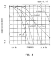
- Fig. 3 shows an equivalent circuit of the matching circuit portion when the switching circuit is in an ON state.
- parasitic inductances such as bonding wires or the like existing at portions of input and output terminals RF1, RF2 for a high-frequency signal are represented by L1, L2, respectively, and the ON resistance of the FET is supposed to be 0 for simplifying the explanation.
- a capacitance C total1 represents a composite capacitance of the capacitance C1 and a parasitic capacitance C'
- a capacitance C total2 represents a composite capacitance of the capacitance C2 and a parasitic capacitance C''.
- a matching frequency f 1/(2 ⁇ L)((2L-CR 2 )/C) 0.5
- L is 2 [nH] and C is 1 [pF]
- the matching frequency f will be 3.1 [GHz] from this expression.
- a simulation result of the frequency characteristic of the insertion loss will be shown in Fig. 4 in the case where the parasitic inductance L of the switching circuit 1 is 1 [nH] and the value C is changed.
- This simulation result is an example where a GaAs field junction type FET (JFET) having a gate width of 1 [mm] and a gate length 0.5 [ ⁇ m] is employed as an FET.
- JFET GaAs field junction type FET
- the insertion loss can be decreased in the frequency range of several [GHz] even when the matching capacitance is 1 [pF] at most.
- the parasitic inductance of the bonding wire or the like is several [nH].
- the capacitance of about 1 [pF] can be realized by a square capacitor each side being about 100 [ ⁇ m]. Accordingly, an area of the matching capacitor on a semiconductor chip can be made very small.
- the insertion loss can be decreased at a desired frequency.
- the present invention is applied to the switching circuit 1 having both the biasing circuit portion 2 and the matching circuit portion 3.
- the present invention is not limited thereto but may be applied to the switching circuit having only the matching circuit portion 3.
- the high-impedance element is connected to each of the drain and source terminals of the FET1.
- the present invention is not limited thereto but may be applied to a case where a high-impedance element is connected to one of the drain and source terminals.
- the capacitor C1 is connected between the drain terminal of the FET1 and the ground and the capacitor C2 is connected between the source terminal of the FET1 and the ground.
- the present invention is not limited thereto but may be applied to a case where only one capacitor is connected between the ground and one of the drain and source terminals of the FET1.
- a single gate FET is used as the FET1.
- the present invention is not limited thereto but may be widely applied to a case where a dual gate FET or a multi-gate FET is used as the FET1.
- junction type FET is used as the FET1.
- the present invention is not limited thereto but may be applied to a case where a metal semiconductor junction (MES) FET is used as the FET1.
- MES metal semiconductor junction
- the present invention is applied to the basic switching circuit 1.
- the present invention is not limited thereto but may be applied to a composite type switching circuit formed by combining a plurality of the switching circuits 1.
- the present invention may be applied to a composite type switching circuit in which the switching circuit 1 is arranged in series with a signal path and the other switching circuit 1 is arranged between the signal path and the ground.
- the first capacitor is connected between the drain terminal of the field effect transistor and the ground and/or the second capacitor is connected between the source terminal of the field effect transistor and the ground, and the capacitances of the first and/or second capacitances are set in accordance with the signal characteristic. Accordingly, there can be realized a switching circuit which is low in insertion loss at a desired frequency.
- the biasing circuit for generating the bias voltage from the control voltage applied to the two control terminals is provided in addition to the switching circuit using the field effect transistor, the switching circuit can be realized which is able to eliminate a dedicated bias terminal even at the case of using a positive power source and is excellent in isolation property.
Landscapes
- Engineering & Computer Science (AREA)
- Computer Networks & Wireless Communication (AREA)
- Signal Processing (AREA)
- Electronic Switches (AREA)
Applications Claiming Priority (3)
| Application Number | Priority Date | Filing Date | Title |
|---|---|---|---|
| JP7027308A JPH08204528A (ja) | 1995-01-23 | 1995-01-23 | スイツチ回路及び複合スイツチ回路 |
| JP27308/95 | 1995-01-23 | ||
| JP2730895 | 1995-01-23 |
Publications (3)
| Publication Number | Publication Date |
|---|---|
| EP0723337A2 true EP0723337A2 (de) | 1996-07-24 |
| EP0723337A3 EP0723337A3 (de) | 1997-04-23 |
| EP0723337B1 EP0723337B1 (de) | 2000-06-28 |
Family
ID=12217465
Family Applications (1)
| Application Number | Title | Priority Date | Filing Date |
|---|---|---|---|
| EP96100844A Expired - Lifetime EP0723337B1 (de) | 1995-01-23 | 1996-01-22 | Schalter und diesen enthaltende Schaltungsanordnung |
Country Status (5)
| Country | Link |
|---|---|
| US (1) | US5717356A (de) |
| EP (1) | EP0723337B1 (de) |
| JP (1) | JPH08204528A (de) |
| KR (1) | KR100389465B1 (de) |
| DE (1) | DE69608973T2 (de) |
Cited By (3)
| Publication number | Priority date | Publication date | Assignee | Title |
|---|---|---|---|---|
| EP1335492A2 (de) | 2002-02-08 | 2003-08-13 | Delphi Technologies, Inc. | Isolierte Gate-Treiberschaltung mit einem getakteten Eingangskondensator |
| EP1469602A3 (de) * | 2003-04-16 | 2004-11-17 | Matsushita Electric Industrial Co., Ltd. | Hochfrequenz-Schaltkreis |
| EP2403134A3 (de) * | 2010-06-23 | 2015-07-01 | Richwave Technology Corp. | Vorrichtung und Verfahren zur digitalen Kapazitätssteuerung |
Families Citing this family (50)
| Publication number | Priority date | Publication date | Assignee | Title |
|---|---|---|---|---|
| JPH0927736A (ja) * | 1995-07-13 | 1997-01-28 | Japan Radio Co Ltd | Fetスイッチ |
| JP3831575B2 (ja) | 2000-05-15 | 2006-10-11 | 三洋電機株式会社 | 化合物半導体スイッチ回路装置 |
| US6580107B2 (en) | 2000-10-10 | 2003-06-17 | Sanyo Electric Co., Ltd. | Compound semiconductor device with depletion layer stop region |
| JP2002289790A (ja) | 2001-03-27 | 2002-10-04 | Sanyo Electric Co Ltd | 化合物半導体スイッチ回路装置 |
| TW530455B (en) | 2001-04-19 | 2003-05-01 | Sanyo Electric Co | Switch circuit device of compound semiconductor |
| US6804502B2 (en) | 2001-10-10 | 2004-10-12 | Peregrine Semiconductor Corporation | Switch circuit and method of switching radio frequency signals |
| KR100442669B1 (ko) * | 2002-02-18 | 2004-08-02 | 삼성전자주식회사 | 세라믹 커패시터의 고주파 특성 개선방법 및 이를 이용한 디씨 블록 |
| US7250804B2 (en) * | 2002-12-17 | 2007-07-31 | M/A -Com, Inc. | Series/shunt switch and method of control |
| US6903596B2 (en) * | 2003-03-17 | 2005-06-07 | Mitsubishi Electric & Electronics U.S.A., Inc. | Method and system for impedance matched switching |
| JP2005006072A (ja) | 2003-06-12 | 2005-01-06 | Matsushita Electric Ind Co Ltd | 高周波スイッチ装置および半導体装置 |
| JP2005006143A (ja) | 2003-06-13 | 2005-01-06 | Matsushita Electric Ind Co Ltd | 高周波スイッチ回路および半導体装置 |
| JP4659826B2 (ja) | 2004-06-23 | 2011-03-30 | ペレグリン セミコンダクター コーポレーション | Rfフロントエンド集積回路 |
| JP2006332416A (ja) * | 2005-05-27 | 2006-12-07 | Nec Electronics Corp | 半導体装置 |
| US20080076371A1 (en) | 2005-07-11 | 2008-03-27 | Alexander Dribinsky | Circuit and method for controlling charge injection in radio frequency switches |
| US7910993B2 (en) | 2005-07-11 | 2011-03-22 | Peregrine Semiconductor Corporation | Method and apparatus for use in improving linearity of MOSFET's using an accumulated charge sink |
| US7890891B2 (en) | 2005-07-11 | 2011-02-15 | Peregrine Semiconductor Corporation | Method and apparatus improving gate oxide reliability by controlling accumulated charge |
| US9653601B2 (en) | 2005-07-11 | 2017-05-16 | Peregrine Semiconductor Corporation | Method and apparatus for use in improving linearity of MOSFETs using an accumulated charge sink-harmonic wrinkle reduction |
| USRE48965E1 (en) | 2005-07-11 | 2022-03-08 | Psemi Corporation | Method and apparatus improving gate oxide reliability by controlling accumulated charge |
| US8742502B2 (en) | 2005-07-11 | 2014-06-03 | Peregrine Semiconductor Corporation | Method and apparatus for use in improving linearity of MOSFETs using an accumulated charge sink-harmonic wrinkle reduction |
| WO2008114455A1 (ja) * | 2007-03-21 | 2008-09-25 | Fujitsu Microelectronics Limited | スイッチング容量生成回路 |
| JP4538016B2 (ja) * | 2007-03-23 | 2010-09-08 | パナソニック株式会社 | 高周波スイッチ装置および半導体装置 |
| US7960772B2 (en) * | 2007-04-26 | 2011-06-14 | Peregrine Semiconductor Corporation | Tuning capacitance to enhance FET stack voltage withstand |
| JP2009201096A (ja) * | 2008-01-22 | 2009-09-03 | Nec Electronics Corp | スイッチ回路 |
| JP5417346B2 (ja) | 2008-02-28 | 2014-02-12 | ペレグリン セミコンダクター コーポレーション | 集積回路素子内でキャパシタをデジタル処理で同調するときに用いられる方法及び装置 |
| US8723260B1 (en) | 2009-03-12 | 2014-05-13 | Rf Micro Devices, Inc. | Semiconductor radio frequency switch with body contact |
| US7952419B1 (en) * | 2009-11-16 | 2011-05-31 | Analog Devices, Inc. | Bootstrapped switch circuit |
| US8604862B2 (en) | 2009-11-16 | 2013-12-10 | Analog Devices, Inc. | Four-quadrant bootstrapped switch circuit |
| JP5366911B2 (ja) * | 2010-10-18 | 2013-12-11 | パナソニック株式会社 | 高周波用スイッチ回路 |
| US9543929B2 (en) | 2012-01-06 | 2017-01-10 | Richwave Technology Corp. | Apparatus and method for obtaining power voltage from control signals |
| US9231578B2 (en) * | 2012-01-06 | 2016-01-05 | Richwave Technology Corp. | Apparatus and method for obtaining auxiliary voltage from control signals |
| KR101378866B1 (ko) * | 2012-08-23 | 2014-03-27 | 주식회사 하이딥 | 저전력 rf 스위치 |
| US9590674B2 (en) | 2012-12-14 | 2017-03-07 | Peregrine Semiconductor Corporation | Semiconductor devices with switchable ground-body connection |
| US20150236748A1 (en) | 2013-03-14 | 2015-08-20 | Peregrine Semiconductor Corporation | Devices and Methods for Duplexer Loss Reduction |
| CN104242881A (zh) * | 2013-06-24 | 2014-12-24 | 瑞昱半导体股份有限公司 | 半导体开关 |
| US9917575B2 (en) * | 2013-07-08 | 2018-03-13 | Infineon Technologies Ag | Circuit comprising an accelerating element |
| US9406695B2 (en) | 2013-11-20 | 2016-08-02 | Peregrine Semiconductor Corporation | Circuit and method for improving ESD tolerance and switching speed |
| US10097171B2 (en) * | 2014-07-25 | 2018-10-09 | Rfaxis, Inc. | Radio frequency switch with low oxide stress |
| US9831857B2 (en) | 2015-03-11 | 2017-11-28 | Peregrine Semiconductor Corporation | Power splitter with programmable output phase shift |
| US9621152B2 (en) * | 2015-05-14 | 2017-04-11 | The Regents Of The University Of California | Coupling inductor based hybrid millimeter-wave switch |
| US9948281B2 (en) | 2016-09-02 | 2018-04-17 | Peregrine Semiconductor Corporation | Positive logic digitally tunable capacitor |
| CN107947775A (zh) * | 2017-12-13 | 2018-04-20 | 上海华虹宏力半导体制造有限公司 | 一种改善关断电容的射频开关电路 |
| US10886911B2 (en) | 2018-03-28 | 2021-01-05 | Psemi Corporation | Stacked FET switch bias ladders |
| US10505530B2 (en) | 2018-03-28 | 2019-12-10 | Psemi Corporation | Positive logic switch with selectable DC blocking circuit |
| US10236872B1 (en) | 2018-03-28 | 2019-03-19 | Psemi Corporation | AC coupling modules for bias ladders |
| TWI676366B (zh) | 2018-08-10 | 2019-11-01 | 立積電子股份有限公司 | 射頻裝置及其電壓產生電路 |
| TWI734221B (zh) * | 2019-10-16 | 2021-07-21 | 立積電子股份有限公司 | 射頻裝置及其電壓產生裝置 |
| CN115085759B (zh) | 2019-10-17 | 2024-10-01 | 立积电子股份有限公司 | 射频装置 |
| US11476849B2 (en) | 2020-01-06 | 2022-10-18 | Psemi Corporation | High power positive logic switch |
| US11437992B2 (en) | 2020-07-30 | 2022-09-06 | Mobix Labs, Inc. | Low-loss mm-wave CMOS resonant switch |
| TWI819264B (zh) | 2020-12-25 | 2023-10-21 | 立積電子股份有限公司 | 射頻裝置及其電壓產生與諧波抑制器 |
Family Cites Families (21)
| Publication number | Priority date | Publication date | Assignee | Title |
|---|---|---|---|---|
| MX152678A (es) * | 1982-04-07 | 1985-10-07 | Int Standard Electric Corp | Mejoras en circuito para un relevador electronico integrable de estado solido |
| JPS5954258A (ja) * | 1982-09-21 | 1984-03-29 | Matsushita Electronics Corp | 半導体電子スイツチ |
| JPS6074718A (ja) * | 1983-09-30 | 1985-04-27 | Hitachi Ltd | 直流バイアス回路 |
| GB2157521A (en) * | 1984-04-14 | 1985-10-23 | Video Interactive Systems Ltd | Improvements relating to interface circuits |
| JPS6215924A (ja) * | 1985-07-12 | 1987-01-24 | Matsushita Electric Works Ltd | 半導体リレ−回路 |
| US4918401A (en) * | 1985-09-30 | 1990-04-17 | Siemens Aktiengesellschaft | Step adjustable distributed amplifier network structure |
| JPS62296617A (ja) * | 1986-06-16 | 1987-12-23 | Matsushita Electric Works Ltd | 半導体リレ−回路 |
| CH675181A5 (de) * | 1988-05-19 | 1990-08-31 | Siemens Ag Albis | |
| EP0360916A1 (de) * | 1988-09-30 | 1990-04-04 | Siemens Aktiengesellschaft | Monolithisch integrierbares Mirkowellen-Dämpfungsglied |
| US4983865A (en) * | 1989-01-25 | 1991-01-08 | Pacific Monolithics | High speed switch matrix |
| JPH0349401A (ja) * | 1989-07-18 | 1991-03-04 | Mitsubishi Electric Corp | マイクロ波素子 |
| JPH0773202B2 (ja) * | 1989-12-28 | 1995-08-02 | 三菱電機株式会社 | 半導体集積回路 |
| EP0476124A1 (de) * | 1990-03-28 | 1992-03-25 | Varian Associates, Inc. | Mikrowellenschaltung mit feldeffektkreisen |
| JP2519342B2 (ja) * | 1990-06-04 | 1996-07-31 | 株式会社東芝 | 出力回路装置 |
| US5264736A (en) * | 1992-04-28 | 1993-11-23 | Raytheon Company | High frequency resonant gate drive for a power MOSFET |
| JPH05343972A (ja) * | 1992-06-10 | 1993-12-24 | Matsushita Electric Works Ltd | 半導体リレー回路 |
| US5281928A (en) * | 1992-10-26 | 1994-01-25 | M/A-Com, Inc. | Electronic attenuator |
| JP3243892B2 (ja) * | 1993-05-21 | 2002-01-07 | ソニー株式会社 | 信号切り替え用スイッチ |
| JP3362931B2 (ja) * | 1993-09-30 | 2003-01-07 | ソニー株式会社 | アツテネータ回路 |
| US5510747A (en) * | 1993-11-30 | 1996-04-23 | Siliconix Incorporated | Gate drive technique for a bidirectional blocking lateral MOSFET |
| JPH07321587A (ja) * | 1994-03-28 | 1995-12-08 | Toshiba Corp | 減衰装置 |
-
1995
- 1995-01-23 JP JP7027308A patent/JPH08204528A/ja active Pending
-
1996
- 1996-01-20 KR KR1019960001194A patent/KR100389465B1/ko not_active Expired - Fee Related
- 1996-01-22 EP EP96100844A patent/EP0723337B1/de not_active Expired - Lifetime
- 1996-01-22 DE DE69608973T patent/DE69608973T2/de not_active Expired - Fee Related
- 1996-01-23 US US08/590,172 patent/US5717356A/en not_active Expired - Fee Related
Cited By (5)
| Publication number | Priority date | Publication date | Assignee | Title |
|---|---|---|---|---|
| EP1335492A2 (de) | 2002-02-08 | 2003-08-13 | Delphi Technologies, Inc. | Isolierte Gate-Treiberschaltung mit einem getakteten Eingangskondensator |
| EP1335492A3 (de) * | 2002-02-08 | 2006-07-05 | Delphi Technologies, Inc. | Isolierte Gate-Treiberschaltung mit einem getakteten Eingangskondensator |
| EP1469602A3 (de) * | 2003-04-16 | 2004-11-17 | Matsushita Electric Industrial Co., Ltd. | Hochfrequenz-Schaltkreis |
| US7106121B2 (en) | 2003-04-16 | 2006-09-12 | Matsushita Electric Industrial Co., Ltd. | High frequency switch circuit |
| EP2403134A3 (de) * | 2010-06-23 | 2015-07-01 | Richwave Technology Corp. | Vorrichtung und Verfahren zur digitalen Kapazitätssteuerung |
Also Published As
| Publication number | Publication date |
|---|---|
| EP0723337B1 (de) | 2000-06-28 |
| KR100389465B1 (ko) | 2003-09-13 |
| JPH08204528A (ja) | 1996-08-09 |
| EP0723337A3 (de) | 1997-04-23 |
| DE69608973D1 (de) | 2000-08-03 |
| US5717356A (en) | 1998-02-10 |
| KR960030546A (ko) | 1996-08-17 |
| DE69608973T2 (de) | 2000-11-30 |
Similar Documents
| Publication | Publication Date | Title |
|---|---|---|
| EP0723337B1 (de) | Schalter und diesen enthaltende Schaltungsanordnung | |
| JP3332194B2 (ja) | スイツチ半導体集積回路及び通信端末装置 | |
| US5969560A (en) | Switching circuit at high frequency with low insertion loss | |
| JP3441236B2 (ja) | 半導体集積回路装置 | |
| US8451044B2 (en) | Switching circuit | |
| JP3249393B2 (ja) | スイッチ回路 | |
| JP2964975B2 (ja) | 高周波スイッチ回路 | |
| US6882829B2 (en) | Integrated circuit incorporating RF antenna switch and power amplifier | |
| EP0782267A2 (de) | Halbleiterschalter | |
| US20010040479A1 (en) | Electronic switch | |
| JPH11112316A (ja) | Mesfetを用いたスイッチ回路 | |
| JPH07303001A (ja) | 高周波スイッチ | |
| US5416660A (en) | Package for microwave device | |
| KR100582621B1 (ko) | 스위치 회로 장치 | |
| JP3238616B2 (ja) | 半導体スイッチ回路 | |
| JPH08213893A (ja) | 半導体集積回路 | |
| JP3137055B2 (ja) | 半導体スイッチ回路、この回路の制御方法及びアッテネータ回路 | |
| JPH08213891A (ja) | 信号切換え装置 | |
| US5406151A (en) | Semiconductor switching circuit | |
| CN116582119A (zh) | 集成在rfic中的具有旁路功能的天线调谐开关和系统 | |
| JPH10256850A (ja) | 半導体装置及び高周波電力増幅器 | |
| JP3342791B2 (ja) | 高周波単極双投スイッチ | |
| JPH11234106A (ja) | Rf信号スイッチ回路 | |
| JPH0278317A (ja) | 信号切替回路 | |
| JP2000013208A (ja) | バイアス回路内蔵型スイッチic |
Legal Events
| Date | Code | Title | Description |
|---|---|---|---|
| PUAI | Public reference made under article 153(3) epc to a published international application that has entered the european phase |
Free format text: ORIGINAL CODE: 0009012 |
|
| AK | Designated contracting states |
Kind code of ref document: A2 Designated state(s): DE FR GB |
|
| PUAL | Search report despatched |
Free format text: ORIGINAL CODE: 0009013 |
|
| AK | Designated contracting states |
Kind code of ref document: A3 Designated state(s): DE FR GB |
|
| 17P | Request for examination filed |
Effective date: 19970923 |
|
| 17Q | First examination report despatched |
Effective date: 19971128 |
|
| GRAG | Despatch of communication of intention to grant |
Free format text: ORIGINAL CODE: EPIDOS AGRA |
|
| GRAG | Despatch of communication of intention to grant |
Free format text: ORIGINAL CODE: EPIDOS AGRA |
|
| GRAG | Despatch of communication of intention to grant |
Free format text: ORIGINAL CODE: EPIDOS AGRA |
|
| GRAH | Despatch of communication of intention to grant a patent |
Free format text: ORIGINAL CODE: EPIDOS IGRA |
|
| GRAH | Despatch of communication of intention to grant a patent |
Free format text: ORIGINAL CODE: EPIDOS IGRA |
|
| GRAA | (expected) grant |
Free format text: ORIGINAL CODE: 0009210 |
|
| AK | Designated contracting states |
Kind code of ref document: B1 Designated state(s): DE FR GB |
|
| REF | Corresponds to: |
Ref document number: 69608973 Country of ref document: DE Date of ref document: 20000803 |
|
| ET | Fr: translation filed | ||
| PLBE | No opposition filed within time limit |
Free format text: ORIGINAL CODE: 0009261 |
|
| STAA | Information on the status of an ep patent application or granted ep patent |
Free format text: STATUS: NO OPPOSITION FILED WITHIN TIME LIMIT |
|
| 26N | No opposition filed | ||
| REG | Reference to a national code |
Ref country code: GB Ref legal event code: IF02 |
|
| PGFP | Annual fee paid to national office [announced via postgrant information from national office to epo] |
Ref country code: DE Payment date: 20090115 Year of fee payment: 14 |
|
| PGFP | Annual fee paid to national office [announced via postgrant information from national office to epo] |
Ref country code: GB Payment date: 20090121 Year of fee payment: 14 |
|
| PGFP | Annual fee paid to national office [announced via postgrant information from national office to epo] |
Ref country code: FR Payment date: 20090113 Year of fee payment: 14 |
|
| GBPC | Gb: european patent ceased through non-payment of renewal fee |
Effective date: 20100122 |
|
| REG | Reference to a national code |
Ref country code: FR Ref legal event code: ST Effective date: 20100930 |
|
| PG25 | Lapsed in a contracting state [announced via postgrant information from national office to epo] |
Ref country code: FR Free format text: LAPSE BECAUSE OF NON-PAYMENT OF DUE FEES Effective date: 20100201 |
|
| PG25 | Lapsed in a contracting state [announced via postgrant information from national office to epo] |
Ref country code: DE Free format text: LAPSE BECAUSE OF NON-PAYMENT OF DUE FEES Effective date: 20100803 |
|
| PG25 | Lapsed in a contracting state [announced via postgrant information from national office to epo] |
Ref country code: GB Free format text: LAPSE BECAUSE OF NON-PAYMENT OF DUE FEES Effective date: 20100122 |