EP0729181B1 - Harzvergossenes Halbleiterbauteil und dessen Herstellungsverfahren - Google Patents
Harzvergossenes Halbleiterbauteil und dessen Herstellungsverfahren Download PDFInfo
- Publication number
- EP0729181B1 EP0729181B1 EP19960102859 EP96102859A EP0729181B1 EP 0729181 B1 EP0729181 B1 EP 0729181B1 EP 19960102859 EP19960102859 EP 19960102859 EP 96102859 A EP96102859 A EP 96102859A EP 0729181 B1 EP0729181 B1 EP 0729181B1
- Authority
- EP
- European Patent Office
- Prior art keywords
- heat radiator
- semiconductor element
- bonding layer
- layer
- mounting surface
- Prior art date
- Legal status (The legal status is an assumption and is not a legal conclusion. Google has not performed a legal analysis and makes no representation as to the accuracy of the status listed.)
- Expired - Lifetime
Links
Images



Classifications
-
- H—ELECTRICITY
- H10—SEMICONDUCTOR DEVICES; ELECTRIC SOLID-STATE DEVICES NOT OTHERWISE PROVIDED FOR
- H10W—GENERIC PACKAGES, INTERCONNECTIONS, CONNECTORS OR OTHER CONSTRUCTIONAL DETAILS OF DEVICES COVERED BY CLASS H10
- H10W76/00—Containers; Fillings or auxiliary members therefor; Seals
- H10W76/10—Containers or parts thereof
- H10W76/17—Containers or parts thereof characterised by their materials
-
- H—ELECTRICITY
- H10—SEMICONDUCTOR DEVICES; ELECTRIC SOLID-STATE DEVICES NOT OTHERWISE PROVIDED FOR
- H10W—GENERIC PACKAGES, INTERCONNECTIONS, CONNECTORS OR OTHER CONSTRUCTIONAL DETAILS OF DEVICES COVERED BY CLASS H10
- H10W40/00—Arrangements for thermal protection or thermal control
- H10W40/70—Fillings or auxiliary members in containers or in encapsulations for thermal protection or control
- H10W40/77—Auxiliary members characterised by their shape
- H10W40/778—Auxiliary members characterised by their shape in encapsulations
-
- H—ELECTRICITY
- H10—SEMICONDUCTOR DEVICES; ELECTRIC SOLID-STATE DEVICES NOT OTHERWISE PROVIDED FOR
- H10W—GENERIC PACKAGES, INTERCONNECTIONS, CONNECTORS OR OTHER CONSTRUCTIONAL DETAILS OF DEVICES COVERED BY CLASS H10
- H10W72/00—Interconnections or connectors in packages
- H10W72/50—Bond wires
- H10W72/541—Dispositions of bond wires
- H10W72/5449—Dispositions of bond wires not being orthogonal to a side surface of the chip, e.g. fan-out arrangements
-
- H—ELECTRICITY
- H10—SEMICONDUCTOR DEVICES; ELECTRIC SOLID-STATE DEVICES NOT OTHERWISE PROVIDED FOR
- H10W—GENERIC PACKAGES, INTERCONNECTIONS, CONNECTORS OR OTHER CONSTRUCTIONAL DETAILS OF DEVICES COVERED BY CLASS H10
- H10W72/00—Interconnections or connectors in packages
- H10W72/50—Bond wires
- H10W72/551—Materials of bond wires
- H10W72/552—Materials of bond wires comprising metals or metalloids, e.g. silver
-
- H—ELECTRICITY
- H10—SEMICONDUCTOR DEVICES; ELECTRIC SOLID-STATE DEVICES NOT OTHERWISE PROVIDED FOR
- H10W—GENERIC PACKAGES, INTERCONNECTIONS, CONNECTORS OR OTHER CONSTRUCTIONAL DETAILS OF DEVICES COVERED BY CLASS H10
- H10W72/00—Interconnections or connectors in packages
- H10W72/90—Bond pads, in general
- H10W72/931—Shapes of bond pads
- H10W72/932—Plan-view shape, i.e. in top view
-
- H—ELECTRICITY
- H10—SEMICONDUCTOR DEVICES; ELECTRIC SOLID-STATE DEVICES NOT OTHERWISE PROVIDED FOR
- H10W—GENERIC PACKAGES, INTERCONNECTIONS, CONNECTORS OR OTHER CONSTRUCTIONAL DETAILS OF DEVICES COVERED BY CLASS H10
- H10W74/00—Encapsulations, e.g. protective coatings
-
- H—ELECTRICITY
- H10—SEMICONDUCTOR DEVICES; ELECTRIC SOLID-STATE DEVICES NOT OTHERWISE PROVIDED FOR
- H10W—GENERIC PACKAGES, INTERCONNECTIONS, CONNECTORS OR OTHER CONSTRUCTIONAL DETAILS OF DEVICES COVERED BY CLASS H10
- H10W90/00—Package configurations
- H10W90/701—Package configurations characterised by the relative positions of pads or connectors relative to package parts
- H10W90/751—Package configurations characterised by the relative positions of pads or connectors relative to package parts of bond wires
- H10W90/756—Package configurations characterised by the relative positions of pads or connectors relative to package parts of bond wires between a chip and a stacked lead frame, conducting package substrate or heat sink
Definitions
- the invention relates to a semiconductor device with a heat radiator and a method of making such a semiconductor device.
- JP 6-53390 discloses a structure in which a heat radiator having a high thermal conductivity is used in place of a die pad. Such a structure can provide a semiconductor device that is superior in heat radiation.
- a semiconductor element is mounted on a heat radiator after the heat radiator has been plated with silver or the like, the thermal or electrical conductivity between the heat radiator and the semiconductor chip can be improved.
- the plating materials such as silver or the like are inferior in resin adhesion property. If the semiconductor device is of resin sealing type, therefore, a gap tends to be formed between the heat radiator and the sealing resin due to inferiority of the adhesion therebetween. If moisture is accumulated in such a gap then when the semiconductor device is heated, the moisture may be expanded into vapor to enlarge the gap, resulting in separation of the heat radiator from the semiconductor chip.
- EP-A-0693 779 discloses a resin sealing type semiconductor device as defined in the pre-characterizing portion of claim 1 and a method as defined in the pre-characterizing portion of claim 8.
- the object of the invention is to provide a resin sealing type semiconductor device which has superior adhesion properties between the heat radiator and the sealing resin and which has superior heat radiating properties, and a method of making such a semiconductor device.
- the bonding layer formed on the heat radiator is smaller than that of the fixing surface of the semiconductor element, the bonding layer will not extend outwardly from the semiconductor element.
- the semiconductor element adheres to the heat radiator by an adhesive layer of silver paste.
- the adhesive layer forms a fillet which diverges to have its planar dimension larger than the fixing surface of the semiconductor element. If the bonding layer has a shape confined within this fillet, the bonding layer 22 will never contact the resin package 40. This provides an improved adhesion property between the resin package and the heat radiator.
- the heat radiator preferably has an electrical conductivity in addition to its good thermal conductivity. Electrically conductive materials include various metals such as gold, silver and copper. It is further preferable that the semiconductor element is electrically connected to the heat radiator through the fixing and mounting surfaces of the semiconductor element and heat radiator. Thus, the semiconductor element may be grounded through the heat radiator if the heat radiator is in negative potential, for example.
- the bonding layer interposed between the fixing and mounting surfaces of the semiconductor element and heat radiator have an electrical conductivity higher than the surface of the heat radiator.
- the electrical conductivity between the fixing and mounting surfaces is thus improved through the bonding layer.
- the heat radiator may be made of copper while the bonding layer is made of silver.
- an electrically conductive layer is formed in an area other than the bonding layer on the mounting surface, the electrically conductive layer having an electrical conductivity higher than the surface of the heat radiator.
- the electrically conductive layer can electrically connect the electrodes of the semiconductor element to the heat radiator or the leads to the heat radiator. Wires can connect the electrodes to the heat radiator, and can connect the leads to the heat radiator. As a result, the flexibility in designing the leads can be improved by electrically connecting the electrodes to the leads through the heat radiator.
- the materials of the electrically conductive layer include various metals such as gold, silver and copper.
- the conductive layer may be disposed continuously around the periphery of the bonding layer or may be formed in a shape of a dot having a diameter equal to that of the connecting wires.
- the electrodes of the semiconductor element or leads can easily be connected with the conductive layer by the connecting wires.
- the contact area between the resin package and the conductive layer can be minimized since the size of the conductive layer is the minimum necessary for connecting the connecting wires and the conductive layer. Since the conductive layer has an inferior adhesion property because of the resin package, the separation of the resin package from the conductive layer can be reduced to a minimum by minimizing the contact area between the resin package and the conductive layer.
- the bonding layer has a thermal conductivity higher than the surface of the heat radiator.
- the semiconductor element can effectively be cooled by efficiently conducting the heat from the semiconductor element to the heat radiator.
- the resin package seals the heat radiator while leaving part of the heat radiator exposed, the efficiency of heat radiation can be further improved.
- Fig. 1 is a schematic sectional view taken along the line I-I in Fig. 2 showing a semiconductor device of the invention.
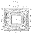
- Fig 2 is a schematic plan view of the semiconductor device without a resin package.
- the semiconductor device comprises a heat radiator 10, a semiconductor element 20 disposed on the heat radiator 10, a plurality of leads 30 and a frame lead 32 disposed outside of the semiconductor element 20. These components are sealed by a resin package 40.
- the heat radiator 10 includes a large portion 12 and a small portion 14 protruding from the large portion 12, forming an inverted T-shape in cross-section.
- the lower surface of the large portion 12 forms a mounting surface 16 on which the semiconductor element 20 is mounted.
- the upper surface of the small portion 14 forms an exposed area since the resin package 40 does not seal the upper surface.
- the heat radiator 10 may be formed of epoxy substrates or ceramics, preferably formed of thermally conductive material such as copper, silver or gold. These metals are also electrically conductive. In this embodiment copper is used for economical considerations.
- a bonding layer 22 is disposed on the mounting surface 16 of the heat radiator 10 .
- the semiconductor element 20 is mounted on the heat radiator 10 through the bonding layer 22.
- the bonding layer 22 is superior in thermal and electrical conductivity line I-I in Fig. 2 showing a semiconductor device of the invention;
- Fig. 2 is a schematic plan view of the semiconductor device of the invention without a resin package
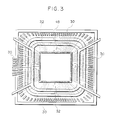
- Fig. 3 illustrates another embodiment of the semiconductor device of the invention
- Fig. 4 illustrates still another embodiment of a semiconductor device of the invention
- Fig. 5 is a diagram showing a process of making the semiconductor device shown in Fig. 4.
- Fig. 1 is a schematic sectional view taken along the line I-I in Fig. 2 showing a semiconductor device of the invention.
- Fig 2 is a schematic plan view of the semiconductor device without a resin package.
- the semiconductor device comprises a heat radiator 10, a semiconductor element 20 disposed on the heat radiator 10, a plurality of leads 30 and a frame lead 32 disposed outside of the semiconductor element 20.
- These components may be formed of silver, gold or platinum, for example. In this embodiment silver is used for economical considerations.
- the bonding layer 22 is thin and equal to a few microns in thickness although it is exaggeratedly shown in Fig. 1 .
- the bonding layer 22 may be formed through sputtering or electro-plating. Alternatively, the bonding layer 22 may be in the form of an embedded thin film or a plate with an electrical conductivity.
- the semiconductor element 20 has a fixing surface 24 which faces the bonding layer 22 and is electrically connected with the bonding layer 22.
- the semiconductor element 20 can electrically be connected with the heat radiator 10 via the fixing surface 24 through the bonding layer 22, because these metals are electrically conductive.
- the bonding layer 22 formed of silver can effectively maintain the electrical connection since the electrical conductivity of the silver is higher than that of the copper.
- the semiconductor element 20 When the semiconductor element 20 is electrically connected with the heat radiator 10 in such a manner, the semiconductor element 20 can easily be grounded through the heat radiator 10 if the heat radiator 10 is in negative potential, for example.
- the length "l" of the bonding layer 22 is smaller than the length "L” of the fixing surface 24 of the semiconductor element 20.
- the bonding layer 22 will never extend beyond the periphery of the fixing surface 24.
- This arrangement is provided because when the bonding layer 22 is formed through silver plating, the silver is inferior in adhesion to a resin which forms the resin package 40.
- the bonding layer 22 extends outwardly from the periphery of the semiconductor element 20, the extended layer portion cannot effectively adhere to the resin package 40. It may be possible that the resin package 40 is separated from the bonding layer 22. In such a case, it is assumed that the electrical connection between the fixing surface 24 of the semiconductor element 20 and the bonding layer 22 is broken. This means that the electrical connection cannot be assured when the fixing surface 24 of the semiconductor element 20 is to be connected to ground (GND) through the bonding layer 22, for example.
- GND ground
- the planar dimension of the bonding layer 22 is formed to be smaller than that of the fixing surface 24 of the semiconductor element 20 so that the bonding layer 22 will never extend beyond the periphery of the fixing surface 24.
- the resin package 40 will not contact the bonding layer 22.
- the resin sealing can completely be made while the electrical connection between the fixing surface 24 of the semiconductor element 20 and the bonding layer 22 is certainly maintained.
- the semiconductor element 20 adheres to the heat radiator 10 by an adhesive layer 26 of silver paste.
- the adhesive layer 26 forms a fillet which diverges to have its planar dimension larger than the fixing surface 24 of the semiconductor element 20. If the bonding layer 22 has a shape confined within this fillet, the bonding layer 22 will never contact the resin package 40.
- the planar dimension of the bonding layer 22 is smaller than that of the fixing surface 24.
- the bonding layer 22 preferably has such a shape that the periphery of the bonding layer 22 is located about 0.05 millimeters inwardly of the periphery of the fixing surface 24.
- a plurality of spot-like conductive layers 18 are formed, spaced away from one another around the semiconductor element 20.
- the conductive layers 18 are formed of a material which is superior in electrical conductivity, such as silver, gold, or platinum. Particularly from the economical viewpoint, this embodiment uses silver.
- the conductive layers 18 are shown exaggeratedly thick in Fig. 1 , they actually are in the form of a thin layer having a thickness equal to a few microns.
- the conductive layers 18 may be formed through any suitable technique, such as sputtering or electro- plating. Alternatively, the conductive layers 18 may be in the form of an embedded silver stud.
- the electrical connection can effectively be maintained by connecting the semiconductor element 20 to the heat radiator 10 through the conductive layers 18, rather than via a direct connection.
- the conductive layers 18 are electrically connected to electrodes 28 in the semiconductor element 20 or to leads 30 via connecting wires 34.
- an insulation layer (not shown) is formed except on the areas on which the bonding layer 22 and conductive layers 18 are formed.
- Such an insulation layer may be formed of any suitable material as far as it has a desired insulation property. It is however preferable that the material is a metal oxide film provided by oxidizing the metal forming the heat radiator 10, for example. If the heat radiator 10 is formed of copper, the surface of the heat radiator 10 may be oxidized by the use of a strong alkaline treating liquid to form an insulation layer. With such an insulation layer, the leads 30 and frame lead 32 can be prevented from short-circuiting with the heat radiator 10. If the insulation layer is formed of copper oxide, it is normally of a dark color such as black or brown. Thus, the leads 30 can easily be recognized using image recognition in the wire bonding process. In addition, the adhesion property of the heat radiator 10 to the resin package 40 can be improved to increase the mechanical strength in the resin package.
- a continuous support 36 is fixed by adhesive.
- the support extends along the periphery of the mounting surface 16 and is formed by a tape-like insulation, for example, a thermosetting resin such as polyimide or epoxy resin.
- the support 36 has so small a width along the periphery of the heat radiator 10 as to support only parts of the leads 30.
- the support 36 made of the aforementioned resin material absorbs moisture by nature, but the amount of the absorbed moisture may be reduced to as little as possible by making the support 36 small.
- the leads 30 are fixedly adhered to the support 36.
- the frame lead 32 is disposed between the semiconductor element 20 and the leads 30 but does not contact the leads 30.
- the frame lead 32 includes four support leads 32a extending outwardly that support the frame lead 32 in a stable manner. Each support lead 32a has a part fixed on the support 36.
- the frame lead 32 functions as a source voltage (Vcc) lead or a reference voltage (Vss) lead. If the frame lead 32 is used as a Vcc lead, the number of necessary power supply leads can greatly be reduced by connecting the power supply electrodes 28 and leads 30 to the frame lead 32 via the connecting wires 34. Thus, the number of signal leads can be increased. This is advantageous since the design flexibility of wiring configurations between the electrodes 28 of the semiconductor element 20 and the leads 30 can be improved.
- a predetermined source voltage or reference voltage can be supplied to any position of the electrodes 28 of the semiconductor element 20.
- the operational speed of the semiconductor element 20 can be accelerated because noise sources are reduced.
- the frame lead 32 is supported by four support leads 32a. Any number and location of the support leads 32a can be selected so long as the support leads 32a can stably support the frame lead 32. For example, two support leads may be provided at two opposite positions.
- the conductive and bonding layers 18, 22 are first formed by silver plating or the like on the mounting surface 16 of the heat radiator 10.
- the formed layers 18 and 22 are masked and then immersed in a bath of oxidizing solution (e.g., "Ebonol" (Trademark) available from MELTEX Co. Ltd.) for a few seconds to form an insulation layer (not shown) on the surface thereof.
- oxidizing solution e.g., "Ebonol" (Trademark) available from MELTEX Co. Ltd.
- the insulation layer thus formed may have a film thickness of 2 microns and an electrical resistivity equal to or higher than 10 13 ⁇ cm. It has been found that such an insulation layer exhibits improved insulation properties.
- the conductive and bonding layers 18, 22 may be formed after the insulation layer has been formed.
- the semiconductor element 20 is then adhered to the bonding layer 22 on the heat radiator 10 through the conductive adhesive layer 26 that may be made of silver paste or the like. Thereafter, the heat radiator 10, the support 36, and a frame (not shown) integrating all the leads 30 and the frame lead 32 are positioned over each other and the above components are thermo-compression bonded and fixed together by the use of an adhesive such as epoxy resin.
- the connecting wires 34 are then bonded in a given pattern by a wire bonding device through the conventional technique.
- the resin package 40 is then formed of epoxy or any other resin around the integral frame through the conventional molding process. At this time, the top surface of the small portion 14 of the heat radiator 10 is left exposed outwardly from the resin package 40.
- the bonding layer 22 has such a configuration that it will never extend outwardly from the fixing surface 24 of the semiconductor element 20. Therefore, the bonding layer 22 will not contact the resin package 40 that is inferior in adhesion to the bonding layer 22. As a result, the semiconductor device of this embodiment will not have a disadvantage due to separation between the resin package 40 and the bonding layer 22.
- Fig. 3 is a schematic plan view showing the primary parts of another embodiment of a semiconductor device constructed in accordance with the invention.
- the shape of a conductive layer 48 of this semiconductor device is different from that of the conductive layer 18 shown in Fig. 2 .
- All the other parts are similar to those of the semiconductor device shown in Fig. 2 . Therefore, they are denoted by similar reference numerals, but will not further be described.
- the conductive layer 48 is formed into a rectangular ring between the leads 30 and the frame lead 32, unlike the spot-like conductive layers 18 shown in Fig. 2 .
- the conductive layer 48 can more easily be electrically connected at any location than a plurality of conductive layers 18.
- Fig. 4 is a schematic plan view showing the primary parts of still another embodiment of a semiconductor device constructed in accordance with the invention.
- the shape of conductive layer 58 of this semiconductor device is different from that of the conductive layer 18 shown in Fig. 2 .
- All the other components are similar to those of the semiconductor device shown in Fig. 2 and designated by similar reference numerals.
- the conductive layer 58 is formed into a dot having the same diameter as that of the connecting wire 34, unlike the spot-like conductive layers 18 shown in Fig. 2 . More particularly, if the diameter of the connecting wire 34 is equal to about 0.8 millimeters, it is preferred that each of the conductive layers 58 has a diameter substantially equal to 0.8 millimeters.
- the conductive layers 58 are formed of silver plating material or the like that is inferior in adhesion to the resin package 40.
- the contact area between the conductive layers 58 and the resin package 40 can be reduced to be as small as possible.
- the conductive layers 58 can more effectively be prevented from being separated from the resin package 40.
- Fig. 5 illustrates a process of forming such extremely small conductive layers 58.
- the conductive layers 58 can be formed through an electro-plating method in which the liquid silver is electro-deposited on the semiconductor device through apertures in a mask. If the diameter of the conductive layers 58 is extremely small, however, the diameter of the apertures in the mask is also extremely small. It is difficult to pass the liquid silver through these apertures in the mask. To overcome such a problem, it may be considered that the mask is reduced in thickness. However, the thinner mask tends to be easily fractured.
- the conductive layers 58 are formed using a mask 60 shown in Fig. 5 .
- the mask 60 includes apertures 66 formed therethrough, each of which has an enlarged-diameter recess 62 formed in the mask 60 on one side and a reduced-diameter recess 64 formed in the mask 60 on the other side, these recesses 62 and 64 communicate with each other.
- the inner wall of each of the apertures 66 between the enlarged-diameter and reduced-diameter recesses 62, 64 is formed to be a step. Alternatively, the inner wall may be tapered.
- the mask 60 is set on the heat radiator 10 with the reduced-diameter recess 64 facing the mounting surface 16 thereof. Liquid silver is then poured onto the mounting surface 16 of the heat radiator 10 from the enlarged-diameter recess 62 through the apertures 66 of the mask 60 to form the dot-like conductive layers 58 having the same diameter as that of the connecting wire 34 through the electro-plating technique.
- the mask 60 Since the mask 60 has the enlarged-diameter recess 62 through which the liquid silver is poured into the apertures 66 of the mask, the liquid silver can easily flow through the apertures 66 of the mask 60. In such a case, the thickness of the mask 60 itself can be increased, if necessary.
Landscapes
- Cooling Or The Like Of Semiconductors Or Solid State Devices (AREA)
- Structures Or Materials For Encapsulating Or Coating Semiconductor Devices Or Solid State Devices (AREA)
Claims (9)
- Halbleiterbauteil des harzgekapselten Typs, aufweisend:ein Halbleiterelement (20), wobei das Halbleiterelement eine Mehrzahl Elektroden (32) und eine Fixieroberfläche (24) zur Verbindung mit einem anderen Element hat;einen Wärmestrahler (10) zum Kühlen des Halbleiterelements (20), wobei der Wärmestrahler (10) eine Anbauoberfläche (16) zum Anbringen des Halbleiterelements (20) hat;eine Verbindungsschicht (22), die sich zwischen der Fixieroberfläche (24) des Halbleiterelements und der Anbauoberfläche (16) des Wärmestrahlers (10) befindet, wobei die Verbindungsschicht (22) auf der Anbauoberfläche (16) angeordnet und kleiner ist als die Fixieroberfläche (24);eine leitfähige Kleberschicht (26), die das Halbleiterelement (20) mit der Anbauoberfläche verbindet; eine Mehrzahl Leiter (30);eine Mehrzahl Drähte (34), wobei mindestens einer der Drähte (34) einen der Leiter (30) mit einer der Elektroden (32) des Halbleiterelements (20) verbindet; undein Harzgehäuse (40), das das Halbleiterelement (20), den Wärmestrahler (10), die Drähte (34) und Teile der Leiter (30) kapselt,dadurch gekennzeichnet, dass die Kleberschicht (26) im Raum zwischen der Fixieroberfläche (24) und der Anbauoberfläche (16) am Umfang der Verbindungsschicht (22) vorgesehen ist und eine Kehlnaht bildet, die sich über den Umfangsrand der Fixieroberfläche (24) des Halbleiterelements (20) hinaus erstreckt.
- Bauteil nach Anspruch 1, bei dem der Wärmestrahler (10) eine hohe elektrische Leitfähigkeit hat, die Fixieroberfläche (24) des Halbleiterelements (20) mit der Anbauoberfläche (16) des Wärmestrahlers (10) elektrisch verbunden ist und die Verbindungsschicht (22) eine höhere elektrische Leitfähigkeit hat als der Wärmestrahler (10).
- Bauteil nach Anspruch 2, das ferner eine leitfähige Schicht (18) aufweist, wobei die leitfähige Schicht (18) eine höhere elektrische Leitfähigkeit hat als der Wärmestrahler (10) und die leitfähige Schicht (18) auf der Anbauoberfläche (16) des Wärmestrahlers (10) angeordnet und von der Verbindungsschicht (22) getrennt ist.
- Bauteil nach Anspruch 3, bei dem die leitfähige Schicht (18) durchgängig um den Umfang der Verbindungsschicht (22) angeordnet ist.
- Bauteil nach Anspruch 3, bei dem die leitfähige Schicht (18) punktförmig ausgebildet ist und der Durchmesser des Punktes gleich ist dem Durchmesser eines der Drähte (34).
- Bauteil nach einem der Ansprüche 1 bis 5, bei dem die Verbindungsschicht (22) eine höhere Wärmeleitfähigkeit hat als der Wärmestrahler (10).
- Bauteil nach einem der Ansprüche 1 bis 6, bei dem das Harzgehäuse (40) den Wärmestrahler (10) kapselt, während ein Abschnitt des Wärmestrahlers (10) freiliegt.
- Verfahren zur Herstellung eines Halbleiterbauteils des harzgekapselten Typs, aufweisend:(a) Anbringen einer Verbindungsschicht (22) auf einer Anbauoberfläche (16) eines Wärmestrahlers (10);(b) Verbinden einer Fixieroberfläche (24) des Halbleiterelements (20) mittels eines leitfähigen Klebemittels mit der Verbindungsschicht (22), wobei die Fixieroberfläche (24) größer ist als die Verbindungsschicht (22);(c) Verbinden einer Mehrzahl Leiter (30) mittels einer Mehrzahl Drähte (34) mit einer Mehrzahl Elektroden (32) des Halbleiterelements (20); und(d) Kapseln des Halbleiterelements (20), des Wärmestrahlers (10), Teilen jedes der Mehrzahl Leiter (30) und der Mehrzahl Drähte (34) mit einem Harz, so dass das Harz ein Harzgehäuse (40) bildet,dadurch gekennzeichnet, dass Schritt (b) die Bereitstellung eines Klebemittels im Raum zwischen der Fixieroberfläche (24) und der Anbauoberfläche (16) am Umfang der Verbindungsschicht (22) aufweist sowie das Ausbilden einer Kehlnaht, die sich über den Umfangsrand der Fixieroberfläche (24) des Halbleiterelements (20) hinaus erstreckt.
- Verfahren nach Anspruch 8, ferner aufweisend:Bereitstellen einer Maske (60), wobei die Maske (60) einen ersten Abschnitt zum Definieren einer ersten Vertiefung (62) in einer ersten Oberfläche der Maske (60) und einen zweiten Abschnitt zum Definieren einer zweiten Vertiefung (64) in einer zweiten Oberfläche der Maske (60) hat, der Durchmesser der ersten Vertiefung (62) größer ist als der Durchmesser der zweiten Vertiefung (64), der Durchmesser der zweiten Vertiefung (64) gleich dem Durchmesser eines Drahtes ist und die erste Vertiefung (62) und die zweite Vertiefung (64) ein Durchgangsloch (66) bilden;Legen der Maske (60) auf die Anbauoberfläche (16) des Wärmestrahlers (10), so dass die zweite Vertiefung (64) zur Anbauoberfläche (16) weist;Bilden einer leitfähigen Schicht (18) auf der Anbauoberfläche (16) des Wärmestrahlers (10) in Form eines Punktes durch das Durchgangsloch (66) der Maske (60) mittels galvanischer Beschichtung;Verbinden der leitfähigen Schicht (18) mit dem Draht; undKapseln des Drahtes mit dem Harz.
Applications Claiming Priority (4)
| Application Number | Priority Date | Filing Date | Title |
|---|---|---|---|
| JP38776/95 | 1995-02-27 | ||
| JP3877695 | 1995-02-27 | ||
| JP323847/95 | 1995-11-16 | ||
| JP32384795A JP3542677B2 (ja) | 1995-02-27 | 1995-11-16 | 樹脂封止型半導体装置およびその製造方法 |
Publications (3)
| Publication Number | Publication Date |
|---|---|
| EP0729181A2 EP0729181A2 (de) | 1996-08-28 |
| EP0729181A3 EP0729181A3 (de) | 1997-08-27 |
| EP0729181B1 true EP0729181B1 (de) | 2009-04-15 |
Family
ID=26378064
Family Applications (1)
| Application Number | Title | Priority Date | Filing Date |
|---|---|---|---|
| EP19960102859 Expired - Lifetime EP0729181B1 (de) | 1995-02-27 | 1996-02-26 | Harzvergossenes Halbleiterbauteil und dessen Herstellungsverfahren |
Country Status (8)
| Country | Link |
|---|---|
| US (1) | US5801435A (de) |
| EP (1) | EP0729181B1 (de) |
| JP (1) | JP3542677B2 (de) |
| KR (1) | KR100414450B1 (de) |
| CN (1) | CN1093984C (de) |
| DE (1) | DE69637900D1 (de) |
| SG (1) | SG38933A1 (de) |
| TW (2) | TW562245U (de) |
Families Citing this family (18)
| Publication number | Priority date | Publication date | Assignee | Title |
|---|---|---|---|---|
| US5808357A (en) * | 1992-06-02 | 1998-09-15 | Fujitsu Limited | Semiconductor device having resin encapsulated package structure |
| JP2891184B2 (ja) * | 1996-06-13 | 1999-05-17 | 日本電気株式会社 | 半導体装置及びその製造方法 |
| TW383508B (en) * | 1996-07-29 | 2000-03-01 | Nichia Kagaku Kogyo Kk | Light emitting device and display |
| FR2764114B1 (fr) * | 1997-06-02 | 2003-04-25 | Sgs Thomson Microelectronics | Dispositif semi-conducteur muni d'un dissipateur thermique |
| US6319757B1 (en) * | 1998-07-08 | 2001-11-20 | Caldus Semiconductor, Inc. | Adhesion and/or encapsulation of silicon carbide-based semiconductor devices on ceramic substrates |
| JP3128548B2 (ja) * | 1999-03-11 | 2001-01-29 | 沖電気工業株式会社 | 半導体装置および半導体装置の製造方法 |
| US6198163B1 (en) * | 1999-10-18 | 2001-03-06 | Amkor Technology, Inc. | Thin leadframe-type semiconductor package having heat sink with recess and exposed surface |
| US20030211062A1 (en) * | 2001-05-07 | 2003-11-13 | Karl Laden | Anhydrous skin cleaners |
| US6396130B1 (en) | 2001-09-14 | 2002-05-28 | Amkor Technology, Inc. | Semiconductor package having multiple dies with independently biased back surfaces |
| JP2003258141A (ja) * | 2002-02-27 | 2003-09-12 | Nec Compound Semiconductor Devices Ltd | 電子部品及びその製造方法 |
| JP3566269B2 (ja) * | 2002-06-07 | 2004-09-15 | 富士通株式会社 | リードフレーム及びその製造方法、及び半導体装置。 |
| JP2004349347A (ja) | 2003-05-20 | 2004-12-09 | Rohm Co Ltd | 半導体装置 |
| US7919853B1 (en) * | 2007-11-01 | 2011-04-05 | Amkor Technology, Inc. | Semiconductor package and fabrication method thereof |
| JP2013183023A (ja) * | 2012-03-01 | 2013-09-12 | Toyota Industries Corp | 電力変換装置 |
| JP2013183022A (ja) | 2012-03-01 | 2013-09-12 | Toyota Industries Corp | 半導体装置および半導体装置の製造方法 |
| JP5308595B1 (ja) * | 2012-11-28 | 2013-10-09 | 新電元工業株式会社 | 樹脂封止型半導体装置の製造方法及び樹脂封止型半導体装置 |
| JP6416996B1 (ja) * | 2017-07-24 | 2018-10-31 | アサヒ・エンジニアリング株式会社 | 樹脂封止装置用の封止型 |
| JP7024349B2 (ja) * | 2017-11-24 | 2022-02-24 | セイコーエプソン株式会社 | センサーユニット、センサーユニットの製造方法、慣性計測装置、電子機器、および移動体 |
Family Cites Families (60)
| Publication number | Priority date | Publication date | Assignee | Title |
|---|---|---|---|---|
| NL280148A (de) * | 1961-06-26 | |||
| US3290564A (en) * | 1963-02-26 | 1966-12-06 | Texas Instruments Inc | Semiconductor device |
| US3965277A (en) * | 1972-05-09 | 1976-06-22 | Massachusetts Institute Of Technology | Photoformed plated interconnection of embedded integrated circuit chips |
| JPS52124865A (en) * | 1976-04-13 | 1977-10-20 | Sharp Corp | Semiconductor device |
| JPS54124678A (en) * | 1978-03-20 | 1979-09-27 | Nec Corp | Lead frame |
| JPS56122134A (en) * | 1980-02-29 | 1981-09-25 | Toshiba Corp | Resin-sealed type semiconductor device |
| JPS5812341A (ja) * | 1981-07-16 | 1983-01-24 | Toshiba Corp | 半導体装置 |
| JPS59207645A (ja) * | 1983-05-11 | 1984-11-24 | Toshiba Corp | 半導体装置およびリ−ドフレ−ム |
| JPS60103651A (ja) * | 1983-11-11 | 1985-06-07 | Hitachi Ltd | 半導体装置 |
| DE3578830D1 (de) * | 1984-06-14 | 1990-08-30 | Advanced Micro Devices Inc | Mehrschicht-waermesenkpackung fuer integrierte schaltung. |
| JPS61166051A (ja) * | 1985-01-17 | 1986-07-26 | Matsushita Electronics Corp | 樹脂封止型半導体装置 |
| JPS6297358A (ja) * | 1985-10-23 | 1987-05-06 | Mitsubishi Electric Corp | 樹脂封止形半導体集積回路装置 |
| US4684975A (en) * | 1985-12-16 | 1987-08-04 | National Semiconductor Corporation | Molded semiconductor package having improved heat dissipation |
| JPS63179557A (ja) * | 1987-01-20 | 1988-07-23 | Nec Corp | 半導体装置用リ−ドフレ−ム |
| JPS63240053A (ja) * | 1987-03-27 | 1988-10-05 | Mitsubishi Electric Corp | 半導体装置 |
| US4942497A (en) * | 1987-07-24 | 1990-07-17 | Nec Corporation | Cooling structure for heat generating electronic components mounted on a substrate |
| US4903118A (en) * | 1988-03-30 | 1990-02-20 | Director General, Agency Of Industrial Science And Technology | Semiconductor device including a resilient bonding resin |
| JPH023390A (ja) * | 1988-06-15 | 1990-01-08 | Brother Ind Ltd | 画像転写形成方法及び画像転写物 |
| US5050040A (en) * | 1988-10-21 | 1991-09-17 | Texas Instruments Incorporated | Composite material, a heat-dissipating member using the material in a circuit system, the circuit system |
| JP2593702B2 (ja) * | 1988-11-09 | 1997-03-26 | 株式会社日立製作所 | 半導体装置の製造方法 |
| US5157478A (en) * | 1989-04-19 | 1992-10-20 | Mitsubishi Denki Kabushiki Kaisha | Tape automated bonding packaged semiconductor device incorporating a heat sink |
| JPH02307251A (ja) * | 1989-05-22 | 1990-12-20 | Nec Corp | 樹脂封止型半導体装置 |
| US5208188A (en) * | 1989-10-02 | 1993-05-04 | Advanced Micro Devices, Inc. | Process for making a multilayer lead frame assembly for an integrated circuit structure and multilayer integrated circuit die package formed by such process |
| JPH03149865A (ja) * | 1989-11-07 | 1991-06-26 | Matsushita Electron Corp | リードフレーム |
| JPH0719876B2 (ja) * | 1989-12-04 | 1995-03-06 | 株式会社東芝 | 半導体装置 |
| JP2517691B2 (ja) * | 1990-01-29 | 1996-07-24 | 三菱電機株式会社 | 半導体装置及びその製造方法 |
| JPH03265161A (ja) * | 1990-03-15 | 1991-11-26 | Toshiba Corp | 樹脂封止型半導体装置 |
| JP2886250B2 (ja) * | 1990-03-26 | 1999-04-26 | 株式会社日立製作所 | 半導体装置 |
| JP2850462B2 (ja) * | 1990-03-29 | 1999-01-27 | セイコーエプソン株式会社 | 半導体装置及びその製造方法 |
| JPH0410558A (ja) * | 1990-04-27 | 1992-01-14 | Hitachi Ltd | 放熱体付き半導体装置 |
| JPH0411758A (ja) * | 1990-04-28 | 1992-01-16 | Mitsubishi Electric Corp | 半導体装置 |
| JPH0427145A (ja) * | 1990-05-22 | 1992-01-30 | Seiko Epson Corp | 半導体装置 |
| US5227662A (en) * | 1990-05-24 | 1993-07-13 | Nippon Steel Corporation | Composite lead frame and semiconductor device using the same |
| US5202288A (en) * | 1990-06-01 | 1993-04-13 | Robert Bosch Gmbh | Method of manufacturing an electronic circuit component incorporating a heat sink |
| DE4017697C2 (de) * | 1990-06-01 | 2003-12-11 | Bosch Gmbh Robert | Elektronisches Bauelement, Verfahren zu dessen Herstellung und Verwendung |
| JP2983620B2 (ja) * | 1990-07-20 | 1999-11-29 | 株式会社日立製作所 | 半導体装置及びその製造方法 |
| JP3047986B2 (ja) * | 1990-07-25 | 2000-06-05 | 株式会社日立製作所 | 半導体装置 |
| JP2725448B2 (ja) * | 1990-08-01 | 1998-03-11 | 三菱電機株式会社 | 半導体装置 |
| US5105259A (en) * | 1990-09-28 | 1992-04-14 | Motorola, Inc. | Thermally enhanced semiconductor device utilizing a vacuum to ultimately enhance thermal dissipation |
| JPH04158556A (ja) * | 1990-10-22 | 1992-06-01 | Toshiba Corp | 樹脂封止型半導体装置 |
| JPH04162556A (ja) * | 1990-10-25 | 1992-06-08 | Mitsubishi Electric Corp | リードフレーム及びその製造方法 |
| JP2841854B2 (ja) * | 1990-11-29 | 1998-12-24 | セイコーエプソン株式会社 | 半導体装置 |
| JPH04316357A (ja) * | 1991-04-15 | 1992-11-06 | Sony Corp | 樹脂封止型半導体装置 |
| US5172213A (en) * | 1991-05-23 | 1992-12-15 | At&T Bell Laboratories | Molded circuit package having heat dissipating post |
| JPH05308107A (ja) * | 1991-07-01 | 1993-11-19 | Sumitomo Electric Ind Ltd | 半導体装置及びその製作方法 |
| DE69231790T2 (de) * | 1991-07-01 | 2002-03-07 | Sumitomo Electric Industries, Ltd. | Wärmeabführendes Bauteil und damit versehene Halbleitervorrichtung |
| US5200809A (en) * | 1991-09-27 | 1993-04-06 | Vlsi Technology, Inc. | Exposed die-attach heatsink package |
| JP2602380B2 (ja) * | 1991-10-23 | 1997-04-23 | 富士通株式会社 | 半導体装置及びその製造方法 |
| JPH05211262A (ja) * | 1992-01-08 | 1993-08-20 | Nec Corp | 樹脂封止型半導体装置 |
| US5328870A (en) * | 1992-01-17 | 1994-07-12 | Amkor Electronics, Inc. | Method for forming plastic molded package with heat sink for integrated circuit devices |
| US5262927A (en) * | 1992-02-07 | 1993-11-16 | Lsi Logic Corporation | Partially-molded, PCB chip carrier package |
| JPH06120374A (ja) * | 1992-03-31 | 1994-04-28 | Amkor Electron Inc | 半導体パッケージ構造、半導体パッケージ方法及び半導体パッケージ用放熱板 |
| JP3572628B2 (ja) * | 1992-06-03 | 2004-10-06 | セイコーエプソン株式会社 | 半導体装置及びその製造方法 |
| JP3322429B2 (ja) * | 1992-06-04 | 2002-09-09 | 新光電気工業株式会社 | 半導体装置 |
| US5367196A (en) * | 1992-09-17 | 1994-11-22 | Olin Corporation | Molded plastic semiconductor package including an aluminum alloy heat spreader |
| JPH0697326A (ja) * | 1992-09-14 | 1994-04-08 | Apic Yamada Kk | 半導体装置およびその放熱部材 |
| JPH06295962A (ja) * | 1992-10-20 | 1994-10-21 | Ibiden Co Ltd | 電子部品搭載用基板およびその製造方法並びに電子部品搭載装置 |
| JPH06132444A (ja) * | 1992-10-20 | 1994-05-13 | Hitachi Ltd | 半導体装置 |
| JP3304447B2 (ja) * | 1992-11-17 | 2002-07-22 | イビデン株式会社 | 電子部品搭載用基板 |
| JP3509274B2 (ja) * | 1994-07-13 | 2004-03-22 | セイコーエプソン株式会社 | 樹脂封止型半導体装置およびその製造方法 |
-
1995
- 1995-11-16 JP JP32384795A patent/JP3542677B2/ja not_active Expired - Lifetime
- 1995-12-28 TW TW88201643U patent/TW562245U/zh not_active IP Right Cessation
- 1995-12-28 TW TW86100244A patent/TW387134B/zh not_active IP Right Cessation
-
1996
- 1996-02-16 KR KR1019960003828A patent/KR100414450B1/ko not_active Expired - Fee Related
- 1996-02-26 CN CN96102532A patent/CN1093984C/zh not_active Expired - Fee Related
- 1996-02-26 DE DE69637900T patent/DE69637900D1/de not_active Expired - Lifetime
- 1996-02-26 US US08/607,139 patent/US5801435A/en not_active Expired - Lifetime
- 1996-02-26 EP EP19960102859 patent/EP0729181B1/de not_active Expired - Lifetime
- 1996-02-27 SG SG1996006122A patent/SG38933A1/en unknown
Also Published As
| Publication number | Publication date |
|---|---|
| TW387134B (en) | 2000-04-11 |
| EP0729181A3 (de) | 1997-08-27 |
| US5801435A (en) | 1998-09-01 |
| KR100414450B1 (ko) | 2004-04-03 |
| EP0729181A2 (de) | 1996-08-28 |
| CN1136711A (zh) | 1996-11-27 |
| JPH08298302A (ja) | 1996-11-12 |
| TW562245U (en) | 2003-11-11 |
| SG38933A1 (en) | 1997-04-17 |
| DE69637900D1 (de) | 2009-05-28 |
| JP3542677B2 (ja) | 2004-07-14 |
| CN1093984C (zh) | 2002-11-06 |
Similar Documents
| Publication | Publication Date | Title |
|---|---|---|
| US5801435A (en) | Resin sealing type semiconductor device and method of making the same | |
| EP0848423B1 (de) | Harzverkapselte halbleiteranordnung und herstellungsverfahren dafür | |
| US6002169A (en) | Thermally enhanced tape ball grid array package | |
| US6291271B1 (en) | Method of making semiconductor chip package | |
| EP0693779B1 (de) | Harzvergossenes Halbleiterbauteil und dessen Herstellungsverfahren | |
| EP1466357B1 (de) | Gehäuse zur oberflächenanbringung mit von der trägerplatte beabstandetem chipboden | |
| KR100359399B1 (ko) | 수지밀폐형 반도체 장치 및 그 제조 방법 | |
| JPH10223672A (ja) | 半導体装置 | |
| US6297964B1 (en) | Semiconductor device, method of fabricating the same film carrier tape, circuit board, and electronic apparatus | |
| JPH09199823A (ja) | チップオンボードプリント配線板 | |
| US6101098A (en) | Structure and method for mounting an electric part | |
| GB2301937A (en) | IC package with a ball grid array on a single layer ceramic substrate | |
| JP2000012773A (ja) | 半導体装置及びその製造方法 | |
| HK1013887A (en) | Resin sealing type semiconductor device and method of making the same | |
| JPH02343A (ja) | 電子部品搭載用基板 | |
| JPH05243418A (ja) | プラスチックpga型半導体装置 | |
| JP2000133745A (ja) | 半導体装置 | |
| KR19990013776A (ko) | 반도체 장치 | |
| JP3036484B2 (ja) | 半導体装置とその製造方法 | |
| JPH05109940A (ja) | 混成集積回路 | |
| JPH1022411A (ja) | 半導体装置及びその製造方法 | |
| JP2649251B2 (ja) | 電子部品搭載用基板 | |
| JP2517360B2 (ja) | 電子部品搭載用基板 | |
| JPH0637457A (ja) | プリント配線板の製造方法 | |
| HK1013888B (en) | Resin sealing type semiconductor device and method of making the same |
Legal Events
| Date | Code | Title | Description |
|---|---|---|---|
| PUAI | Public reference made under article 153(3) epc to a published international application that has entered the european phase |
Free format text: ORIGINAL CODE: 0009012 |
|
| AK | Designated contracting states |
Kind code of ref document: A2 Designated state(s): DE FR GB |
|
| PUAL | Search report despatched |
Free format text: ORIGINAL CODE: 0009013 |
|
| AK | Designated contracting states |
Kind code of ref document: A3 Designated state(s): DE FR GB |
|
| 17P | Request for examination filed |
Effective date: 19980122 |
|
| 17Q | First examination report despatched |
Effective date: 19991115 |
|
| GRAP | Despatch of communication of intention to grant a patent |
Free format text: ORIGINAL CODE: EPIDOSNIGR1 |
|
| GRAS | Grant fee paid |
Free format text: ORIGINAL CODE: EPIDOSNIGR3 |
|
| GRAA | (expected) grant |
Free format text: ORIGINAL CODE: 0009210 |
|
| AK | Designated contracting states |
Kind code of ref document: B1 Designated state(s): DE FR GB |
|
| REG | Reference to a national code |
Ref country code: GB Ref legal event code: FG4D |
|
| REF | Corresponds to: |
Ref document number: 69637900 Country of ref document: DE Date of ref document: 20090528 Kind code of ref document: P |
|
| PLBE | No opposition filed within time limit |
Free format text: ORIGINAL CODE: 0009261 |
|
| STAA | Information on the status of an ep patent application or granted ep patent |
Free format text: STATUS: NO OPPOSITION FILED WITHIN TIME LIMIT |
|
| 26N | No opposition filed |
Effective date: 20100118 |
|
| REG | Reference to a national code |
Ref country code: HK Ref legal event code: WD Ref document number: 1013887 Country of ref document: HK |
|
| REG | Reference to a national code |
Ref country code: FR Ref legal event code: ST Effective date: 20101029 |
|
| PG25 | Lapsed in a contracting state [announced via postgrant information from national office to epo] |
Ref country code: FR Free format text: LAPSE BECAUSE OF NON-PAYMENT OF DUE FEES Effective date: 20100301 |
|
| PGFP | Annual fee paid to national office [announced via postgrant information from national office to epo] |
Ref country code: DE Payment date: 20120222 Year of fee payment: 17 |
|
| PGFP | Annual fee paid to national office [announced via postgrant information from national office to epo] |
Ref country code: GB Payment date: 20120222 Year of fee payment: 17 |
|
| GBPC | Gb: european patent ceased through non-payment of renewal fee |
Effective date: 20130226 |
|
| REG | Reference to a national code |
Ref country code: DE Ref legal event code: R119 Ref document number: 69637900 Country of ref document: DE Effective date: 20130903 |
|
| PG25 | Lapsed in a contracting state [announced via postgrant information from national office to epo] |
Ref country code: DE Free format text: LAPSE BECAUSE OF NON-PAYMENT OF DUE FEES Effective date: 20130903 Ref country code: GB Free format text: LAPSE BECAUSE OF NON-PAYMENT OF DUE FEES Effective date: 20130226 |