EP0729181A2 - Harzvergossenes Halbleiterbauteil und dessen Herstellungsverfahren - Google Patents
Harzvergossenes Halbleiterbauteil und dessen Herstellungsverfahren Download PDFInfo
- Publication number
- EP0729181A2 EP0729181A2 EP96102859A EP96102859A EP0729181A2 EP 0729181 A2 EP0729181 A2 EP 0729181A2 EP 96102859 A EP96102859 A EP 96102859A EP 96102859 A EP96102859 A EP 96102859A EP 0729181 A2 EP0729181 A2 EP 0729181A2
- Authority
- EP
- European Patent Office
- Prior art keywords
- heat radiator
- semiconductor element
- bonding layer
- semiconductor device
- resin
- Prior art date
- Legal status (The legal status is an assumption and is not a legal conclusion. Google has not performed a legal analysis and makes no representation as to the accuracy of the status listed.)
- Granted
Links
Images



Classifications
-
- H—ELECTRICITY
- H10—SEMICONDUCTOR DEVICES; ELECTRIC SOLID-STATE DEVICES NOT OTHERWISE PROVIDED FOR
- H10W—GENERIC PACKAGES, INTERCONNECTIONS, CONNECTORS OR OTHER CONSTRUCTIONAL DETAILS OF DEVICES COVERED BY CLASS H10
- H10W76/00—Containers; Fillings or auxiliary members therefor; Seals
- H10W76/10—Containers or parts thereof
- H10W76/17—Containers or parts thereof characterised by their materials
-
- H—ELECTRICITY
- H10—SEMICONDUCTOR DEVICES; ELECTRIC SOLID-STATE DEVICES NOT OTHERWISE PROVIDED FOR
- H10W—GENERIC PACKAGES, INTERCONNECTIONS, CONNECTORS OR OTHER CONSTRUCTIONAL DETAILS OF DEVICES COVERED BY CLASS H10
- H10W40/00—Arrangements for thermal protection or thermal control
- H10W40/70—Fillings or auxiliary members in containers or in encapsulations for thermal protection or control
- H10W40/77—Auxiliary members characterised by their shape
- H10W40/778—Auxiliary members characterised by their shape in encapsulations
-
- H—ELECTRICITY
- H10—SEMICONDUCTOR DEVICES; ELECTRIC SOLID-STATE DEVICES NOT OTHERWISE PROVIDED FOR
- H10W—GENERIC PACKAGES, INTERCONNECTIONS, CONNECTORS OR OTHER CONSTRUCTIONAL DETAILS OF DEVICES COVERED BY CLASS H10
- H10W72/00—Interconnections or connectors in packages
- H10W72/50—Bond wires
- H10W72/541—Dispositions of bond wires
- H10W72/5449—Dispositions of bond wires not being orthogonal to a side surface of the chip, e.g. fan-out arrangements
-
- H—ELECTRICITY
- H10—SEMICONDUCTOR DEVICES; ELECTRIC SOLID-STATE DEVICES NOT OTHERWISE PROVIDED FOR
- H10W—GENERIC PACKAGES, INTERCONNECTIONS, CONNECTORS OR OTHER CONSTRUCTIONAL DETAILS OF DEVICES COVERED BY CLASS H10
- H10W72/00—Interconnections or connectors in packages
- H10W72/50—Bond wires
- H10W72/551—Materials of bond wires
- H10W72/552—Materials of bond wires comprising metals or metalloids, e.g. silver
-
- H—ELECTRICITY
- H10—SEMICONDUCTOR DEVICES; ELECTRIC SOLID-STATE DEVICES NOT OTHERWISE PROVIDED FOR
- H10W—GENERIC PACKAGES, INTERCONNECTIONS, CONNECTORS OR OTHER CONSTRUCTIONAL DETAILS OF DEVICES COVERED BY CLASS H10
- H10W72/00—Interconnections or connectors in packages
- H10W72/90—Bond pads, in general
- H10W72/931—Shapes of bond pads
- H10W72/932—Plan-view shape, i.e. in top view
-
- H—ELECTRICITY
- H10—SEMICONDUCTOR DEVICES; ELECTRIC SOLID-STATE DEVICES NOT OTHERWISE PROVIDED FOR
- H10W—GENERIC PACKAGES, INTERCONNECTIONS, CONNECTORS OR OTHER CONSTRUCTIONAL DETAILS OF DEVICES COVERED BY CLASS H10
- H10W74/00—Encapsulations, e.g. protective coatings
-
- H—ELECTRICITY
- H10—SEMICONDUCTOR DEVICES; ELECTRIC SOLID-STATE DEVICES NOT OTHERWISE PROVIDED FOR
- H10W—GENERIC PACKAGES, INTERCONNECTIONS, CONNECTORS OR OTHER CONSTRUCTIONAL DETAILS OF DEVICES COVERED BY CLASS H10
- H10W90/00—Package configurations
- H10W90/701—Package configurations characterised by the relative positions of pads or connectors relative to package parts
- H10W90/751—Package configurations characterised by the relative positions of pads or connectors relative to package parts of bond wires
- H10W90/756—Package configurations characterised by the relative positions of pads or connectors relative to package parts of bond wires between a chip and a stacked lead frame, conducting package substrate or heat sink
Definitions
- a semiconductor element is mounted on a heat radiator after the heat radiator has been plated with silver or the like, the thermal or electrical conductivity between the heat radiator and the semiconductor chip can be improved.
- the resin package seals the heat radiator while leaving part of the heat radiator exposed, the efficiency of heat radiation can be further improved.
- a mask which has a portion for defining a first recess on one surface of the mask and another portion for defining a second recess on the other surface of the mask.
- the diameter of the first recess is larger than the diameter of the second recess, the diameter of the second recess is similar to the diameter of one of the connecting wires, and the first recess and the second recess form a through hole.
- the conductive layer and electrodes of the semiconductor element are connected via a first set of connecting wires, and connecting leads and electrodes of the semiconductor element are connected via a second set of connecting wires.
- the semiconductor element 20 When the semiconductor element 20 is electrically connected with the heat radiator 10 in such a manner, the semiconductor element 20 can easily be grounded through the heat radiator 10 if the heat radiator 10 is in negative potential, for example.
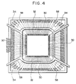
- the frame lead 32 is supported by four support leads 32a. Any number and location of the support leads 32a can be selected so long as the support leads 32a can stably support the frame lead 32. For example, two support leads may be provided at two opposite positions.
- the mask 60 Since the mask 60 has the enlarged-diameter recess 62 through which the liquid silver is poured into the apertures 66 of the mask, the liquid silver can easily flow through the apertures 66 of the mask 60. In such a case, the thickness of the mask 60 itself can be increased, if necessary.
Landscapes
- Cooling Or The Like Of Semiconductors Or Solid State Devices (AREA)
- Structures Or Materials For Encapsulating Or Coating Semiconductor Devices Or Solid State Devices (AREA)
Applications Claiming Priority (4)
| Application Number | Priority Date | Filing Date | Title |
|---|---|---|---|
| JP3877695 | 1995-02-27 | ||
| JP38776/95 | 1995-02-27 | ||
| JP323847/95 | 1995-11-16 | ||
| JP32384795A JP3542677B2 (ja) | 1995-02-27 | 1995-11-16 | 樹脂封止型半導体装置およびその製造方法 |
Publications (3)
| Publication Number | Publication Date |
|---|---|
| EP0729181A2 true EP0729181A2 (de) | 1996-08-28 |
| EP0729181A3 EP0729181A3 (de) | 1997-08-27 |
| EP0729181B1 EP0729181B1 (de) | 2009-04-15 |
Family
ID=26378064
Family Applications (1)
| Application Number | Title | Priority Date | Filing Date |
|---|---|---|---|
| EP19960102859 Expired - Lifetime EP0729181B1 (de) | 1995-02-27 | 1996-02-26 | Harzvergossenes Halbleiterbauteil und dessen Herstellungsverfahren |
Country Status (8)
| Country | Link |
|---|---|
| US (1) | US5801435A (de) |
| EP (1) | EP0729181B1 (de) |
| JP (1) | JP3542677B2 (de) |
| KR (1) | KR100414450B1 (de) |
| CN (1) | CN1093984C (de) |
| DE (1) | DE69637900D1 (de) |
| SG (1) | SG38933A1 (de) |
| TW (2) | TW562245U (de) |
Families Citing this family (18)
| Publication number | Priority date | Publication date | Assignee | Title |
|---|---|---|---|---|
| US5808357A (en) * | 1992-06-02 | 1998-09-15 | Fujitsu Limited | Semiconductor device having resin encapsulated package structure |
| JP2891184B2 (ja) * | 1996-06-13 | 1999-05-17 | 日本電気株式会社 | 半導体装置及びその製造方法 |
| TW383508B (en) * | 1996-07-29 | 2000-03-01 | Nichia Kagaku Kogyo Kk | Light emitting device and display |
| FR2764114B1 (fr) * | 1997-06-02 | 2003-04-25 | Sgs Thomson Microelectronics | Dispositif semi-conducteur muni d'un dissipateur thermique |
| US6319757B1 (en) * | 1998-07-08 | 2001-11-20 | Caldus Semiconductor, Inc. | Adhesion and/or encapsulation of silicon carbide-based semiconductor devices on ceramic substrates |
| JP3128548B2 (ja) * | 1999-03-11 | 2001-01-29 | 沖電気工業株式会社 | 半導体装置および半導体装置の製造方法 |
| US6198163B1 (en) * | 1999-10-18 | 2001-03-06 | Amkor Technology, Inc. | Thin leadframe-type semiconductor package having heat sink with recess and exposed surface |
| US20030211062A1 (en) * | 2001-05-07 | 2003-11-13 | Karl Laden | Anhydrous skin cleaners |
| US6396130B1 (en) | 2001-09-14 | 2002-05-28 | Amkor Technology, Inc. | Semiconductor package having multiple dies with independently biased back surfaces |
| JP2003258141A (ja) * | 2002-02-27 | 2003-09-12 | Nec Compound Semiconductor Devices Ltd | 電子部品及びその製造方法 |
| JP3566269B2 (ja) * | 2002-06-07 | 2004-09-15 | 富士通株式会社 | リードフレーム及びその製造方法、及び半導体装置。 |
| JP2004349347A (ja) | 2003-05-20 | 2004-12-09 | Rohm Co Ltd | 半導体装置 |
| US7919853B1 (en) * | 2007-11-01 | 2011-04-05 | Amkor Technology, Inc. | Semiconductor package and fabrication method thereof |
| JP2013183023A (ja) * | 2012-03-01 | 2013-09-12 | Toyota Industries Corp | 電力変換装置 |
| JP2013183022A (ja) * | 2012-03-01 | 2013-09-12 | Toyota Industries Corp | 半導体装置および半導体装置の製造方法 |
| JP5308595B1 (ja) * | 2012-11-28 | 2013-10-09 | 新電元工業株式会社 | 樹脂封止型半導体装置の製造方法及び樹脂封止型半導体装置 |
| JP6416996B1 (ja) * | 2017-07-24 | 2018-10-31 | アサヒ・エンジニアリング株式会社 | 樹脂封止装置用の封止型 |
| JP7024349B2 (ja) * | 2017-11-24 | 2022-02-24 | セイコーエプソン株式会社 | センサーユニット、センサーユニットの製造方法、慣性計測装置、電子機器、および移動体 |
Family Cites Families (60)
| Publication number | Priority date | Publication date | Assignee | Title |
|---|---|---|---|---|
| NL121811C (de) * | 1961-06-26 | |||
| US3290564A (en) * | 1963-02-26 | 1966-12-06 | Texas Instruments Inc | Semiconductor device |
| US3965277A (en) * | 1972-05-09 | 1976-06-22 | Massachusetts Institute Of Technology | Photoformed plated interconnection of embedded integrated circuit chips |
| JPS52124865A (en) * | 1976-04-13 | 1977-10-20 | Sharp Corp | Semiconductor device |
| JPS54124678A (en) * | 1978-03-20 | 1979-09-27 | Nec Corp | Lead frame |
| JPS56122134A (en) * | 1980-02-29 | 1981-09-25 | Toshiba Corp | Resin-sealed type semiconductor device |
| JPS5812341A (ja) * | 1981-07-16 | 1983-01-24 | Toshiba Corp | 半導体装置 |
| JPS59207645A (ja) * | 1983-05-11 | 1984-11-24 | Toshiba Corp | 半導体装置およびリ−ドフレ−ム |
| JPS60103651A (ja) * | 1983-11-11 | 1985-06-07 | Hitachi Ltd | 半導体装置 |
| EP0164794B1 (de) * | 1984-06-14 | 1990-07-25 | Advanced Micro Devices, Inc. | Mehrschicht-Wärmesenkpackung für integrierte Schaltung |
| JPS61166051A (ja) * | 1985-01-17 | 1986-07-26 | Matsushita Electronics Corp | 樹脂封止型半導体装置 |
| JPS6297358A (ja) * | 1985-10-23 | 1987-05-06 | Mitsubishi Electric Corp | 樹脂封止形半導体集積回路装置 |
| US4684975A (en) * | 1985-12-16 | 1987-08-04 | National Semiconductor Corporation | Molded semiconductor package having improved heat dissipation |
| JPS63179557A (ja) * | 1987-01-20 | 1988-07-23 | Nec Corp | 半導体装置用リ−ドフレ−ム |
| JPS63240053A (ja) * | 1987-03-27 | 1988-10-05 | Mitsubishi Electric Corp | 半導体装置 |
| US4942497A (en) * | 1987-07-24 | 1990-07-17 | Nec Corporation | Cooling structure for heat generating electronic components mounted on a substrate |
| US4903118A (en) * | 1988-03-30 | 1990-02-20 | Director General, Agency Of Industrial Science And Technology | Semiconductor device including a resilient bonding resin |
| JPH023390A (ja) * | 1988-06-15 | 1990-01-08 | Brother Ind Ltd | 画像転写形成方法及び画像転写物 |
| US5050040A (en) * | 1988-10-21 | 1991-09-17 | Texas Instruments Incorporated | Composite material, a heat-dissipating member using the material in a circuit system, the circuit system |
| JP2593702B2 (ja) * | 1988-11-09 | 1997-03-26 | 株式会社日立製作所 | 半導体装置の製造方法 |
| US5157478A (en) * | 1989-04-19 | 1992-10-20 | Mitsubishi Denki Kabushiki Kaisha | Tape automated bonding packaged semiconductor device incorporating a heat sink |
| JPH02307251A (ja) * | 1989-05-22 | 1990-12-20 | Nec Corp | 樹脂封止型半導体装置 |
| US5208188A (en) * | 1989-10-02 | 1993-05-04 | Advanced Micro Devices, Inc. | Process for making a multilayer lead frame assembly for an integrated circuit structure and multilayer integrated circuit die package formed by such process |
| JPH03149865A (ja) * | 1989-11-07 | 1991-06-26 | Matsushita Electron Corp | リードフレーム |
| JPH0719876B2 (ja) * | 1989-12-04 | 1995-03-06 | 株式会社東芝 | 半導体装置 |
| JP2517691B2 (ja) * | 1990-01-29 | 1996-07-24 | 三菱電機株式会社 | 半導体装置及びその製造方法 |
| JPH03265161A (ja) * | 1990-03-15 | 1991-11-26 | Toshiba Corp | 樹脂封止型半導体装置 |
| JP2886250B2 (ja) * | 1990-03-26 | 1999-04-26 | 株式会社日立製作所 | 半導体装置 |
| JP2850462B2 (ja) * | 1990-03-29 | 1999-01-27 | セイコーエプソン株式会社 | 半導体装置及びその製造方法 |
| JPH0410558A (ja) * | 1990-04-27 | 1992-01-14 | Hitachi Ltd | 放熱体付き半導体装置 |
| JPH0411758A (ja) * | 1990-04-28 | 1992-01-16 | Mitsubishi Electric Corp | 半導体装置 |
| JPH0427145A (ja) * | 1990-05-22 | 1992-01-30 | Seiko Epson Corp | 半導体装置 |
| US5227662A (en) * | 1990-05-24 | 1993-07-13 | Nippon Steel Corporation | Composite lead frame and semiconductor device using the same |
| DE4017697C2 (de) * | 1990-06-01 | 2003-12-11 | Bosch Gmbh Robert | Elektronisches Bauelement, Verfahren zu dessen Herstellung und Verwendung |
| US5202288A (en) * | 1990-06-01 | 1993-04-13 | Robert Bosch Gmbh | Method of manufacturing an electronic circuit component incorporating a heat sink |
| JP2983620B2 (ja) * | 1990-07-20 | 1999-11-29 | 株式会社日立製作所 | 半導体装置及びその製造方法 |
| JP3047986B2 (ja) * | 1990-07-25 | 2000-06-05 | 株式会社日立製作所 | 半導体装置 |
| JP2725448B2 (ja) * | 1990-08-01 | 1998-03-11 | 三菱電機株式会社 | 半導体装置 |
| US5105259A (en) * | 1990-09-28 | 1992-04-14 | Motorola, Inc. | Thermally enhanced semiconductor device utilizing a vacuum to ultimately enhance thermal dissipation |
| JPH04158556A (ja) * | 1990-10-22 | 1992-06-01 | Toshiba Corp | 樹脂封止型半導体装置 |
| JPH04162556A (ja) * | 1990-10-25 | 1992-06-08 | Mitsubishi Electric Corp | リードフレーム及びその製造方法 |
| JP2841854B2 (ja) * | 1990-11-29 | 1998-12-24 | セイコーエプソン株式会社 | 半導体装置 |
| JPH04316357A (ja) * | 1991-04-15 | 1992-11-06 | Sony Corp | 樹脂封止型半導体装置 |
| US5172213A (en) * | 1991-05-23 | 1992-12-15 | At&T Bell Laboratories | Molded circuit package having heat dissipating post |
| EP0521405B1 (de) * | 1991-07-01 | 2001-04-18 | Sumitomo Electric Industries, Ltd. | Wärmeabführendes Bauteil und damit versehene Halbleitervorrichtung |
| JPH05308107A (ja) * | 1991-07-01 | 1993-11-19 | Sumitomo Electric Ind Ltd | 半導体装置及びその製作方法 |
| US5200809A (en) * | 1991-09-27 | 1993-04-06 | Vlsi Technology, Inc. | Exposed die-attach heatsink package |
| JP2602380B2 (ja) * | 1991-10-23 | 1997-04-23 | 富士通株式会社 | 半導体装置及びその製造方法 |
| JPH05211262A (ja) * | 1992-01-08 | 1993-08-20 | Nec Corp | 樹脂封止型半導体装置 |
| US5328870A (en) * | 1992-01-17 | 1994-07-12 | Amkor Electronics, Inc. | Method for forming plastic molded package with heat sink for integrated circuit devices |
| US5262927A (en) * | 1992-02-07 | 1993-11-16 | Lsi Logic Corporation | Partially-molded, PCB chip carrier package |
| JPH06120374A (ja) * | 1992-03-31 | 1994-04-28 | Amkor Electron Inc | 半導体パッケージ構造、半導体パッケージ方法及び半導体パッケージ用放熱板 |
| JP3572628B2 (ja) * | 1992-06-03 | 2004-10-06 | セイコーエプソン株式会社 | 半導体装置及びその製造方法 |
| JP3322429B2 (ja) * | 1992-06-04 | 2002-09-09 | 新光電気工業株式会社 | 半導体装置 |
| US5367196A (en) * | 1992-09-17 | 1994-11-22 | Olin Corporation | Molded plastic semiconductor package including an aluminum alloy heat spreader |
| JPH0697326A (ja) * | 1992-09-14 | 1994-04-08 | Apic Yamada Kk | 半導体装置およびその放熱部材 |
| JPH06295962A (ja) * | 1992-10-20 | 1994-10-21 | Ibiden Co Ltd | 電子部品搭載用基板およびその製造方法並びに電子部品搭載装置 |
| JPH06132444A (ja) * | 1992-10-20 | 1994-05-13 | Hitachi Ltd | 半導体装置 |
| JP3304447B2 (ja) * | 1992-11-17 | 2002-07-22 | イビデン株式会社 | 電子部品搭載用基板 |
| JP3509274B2 (ja) * | 1994-07-13 | 2004-03-22 | セイコーエプソン株式会社 | 樹脂封止型半導体装置およびその製造方法 |
-
1995
- 1995-11-16 JP JP32384795A patent/JP3542677B2/ja not_active Expired - Lifetime
- 1995-12-28 TW TW88201643U patent/TW562245U/zh not_active IP Right Cessation
- 1995-12-28 TW TW86100244A patent/TW387134B/zh not_active IP Right Cessation
-
1996
- 1996-02-16 KR KR1019960003828A patent/KR100414450B1/ko not_active Expired - Fee Related
- 1996-02-26 US US08/607,139 patent/US5801435A/en not_active Expired - Lifetime
- 1996-02-26 EP EP19960102859 patent/EP0729181B1/de not_active Expired - Lifetime
- 1996-02-26 CN CN96102532A patent/CN1093984C/zh not_active Expired - Fee Related
- 1996-02-26 DE DE69637900T patent/DE69637900D1/de not_active Expired - Lifetime
- 1996-02-27 SG SG1996006122A patent/SG38933A1/en unknown
Also Published As
| Publication number | Publication date |
|---|---|
| TW387134B (en) | 2000-04-11 |
| EP0729181A3 (de) | 1997-08-27 |
| US5801435A (en) | 1998-09-01 |
| TW562245U (en) | 2003-11-11 |
| CN1093984C (zh) | 2002-11-06 |
| CN1136711A (zh) | 1996-11-27 |
| EP0729181B1 (de) | 2009-04-15 |
| SG38933A1 (en) | 1997-04-17 |
| JP3542677B2 (ja) | 2004-07-14 |
| DE69637900D1 (de) | 2009-05-28 |
| JPH08298302A (ja) | 1996-11-12 |
| KR100414450B1 (ko) | 2004-04-03 |
Similar Documents
| Publication | Publication Date | Title |
|---|---|---|
| US5801435A (en) | Resin sealing type semiconductor device and method of making the same | |
| EP0848423B1 (de) | Harzverkapselte halbleiteranordnung und herstellungsverfahren dafür | |
| US6291271B1 (en) | Method of making semiconductor chip package | |
| US5633529A (en) | Resin sealing type semiconductor device and method of making the same | |
| KR100359399B1 (ko) | 수지밀폐형 반도체 장치 및 그 제조 방법 | |
| KR100420879B1 (ko) | 반도체 장치, 실장기판 및 그 제조방법, 회로기판 및전자기기 | |
| JPH10223672A (ja) | 半導体装置 | |
| US6101098A (en) | Structure and method for mounting an electric part | |
| JP3847839B2 (ja) | 半導体装置 | |
| HK1013887A (en) | Resin sealing type semiconductor device and method of making the same | |
| JPH02343A (ja) | 電子部品搭載用基板 | |
| JP2000133745A (ja) | 半導体装置 | |
| JPH05243418A (ja) | プラスチックpga型半導体装置 | |
| JP3403221B2 (ja) | 配線基板付リードフレーム | |
| JPH05109940A (ja) | 混成集積回路 | |
| JP4400755B2 (ja) | 半導体装置、実装基板及びその製造方法、回路基板並びに電子機器 | |
| JP4396863B2 (ja) | 半導体装置、実装基板及びその製造方法、回路基板並びに電子機器 | |
| JPH03233958A (ja) | 電子部品搭載用基板 | |
| JP2649251B2 (ja) | 電子部品搭載用基板 | |
| JPH1022411A (ja) | 半導体装置及びその製造方法 | |
| JP2517360B2 (ja) | 電子部品搭載用基板 | |
| KR19990013776A (ko) | 반도체 장치 | |
| JP4396862B2 (ja) | 半導体装置、回路基板および電子機器 | |
| JP2000223530A (ja) | フリップチップ実装体および実装方法 | |
| JPH0823049A (ja) | 半導体パッケージ |
Legal Events
| Date | Code | Title | Description |
|---|---|---|---|
| PUAI | Public reference made under article 153(3) epc to a published international application that has entered the european phase |
Free format text: ORIGINAL CODE: 0009012 |
|
| AK | Designated contracting states |
Kind code of ref document: A2 Designated state(s): DE FR GB |
|
| PUAL | Search report despatched |
Free format text: ORIGINAL CODE: 0009013 |
|
| AK | Designated contracting states |
Kind code of ref document: A3 Designated state(s): DE FR GB |
|
| 17P | Request for examination filed |
Effective date: 19980122 |
|
| 17Q | First examination report despatched |
Effective date: 19991115 |
|
| GRAP | Despatch of communication of intention to grant a patent |
Free format text: ORIGINAL CODE: EPIDOSNIGR1 |
|
| GRAS | Grant fee paid |
Free format text: ORIGINAL CODE: EPIDOSNIGR3 |
|
| GRAA | (expected) grant |
Free format text: ORIGINAL CODE: 0009210 |
|
| AK | Designated contracting states |
Kind code of ref document: B1 Designated state(s): DE FR GB |
|
| REG | Reference to a national code |
Ref country code: GB Ref legal event code: FG4D |
|
| REF | Corresponds to: |
Ref document number: 69637900 Country of ref document: DE Date of ref document: 20090528 Kind code of ref document: P |
|
| PLBE | No opposition filed within time limit |
Free format text: ORIGINAL CODE: 0009261 |
|
| STAA | Information on the status of an ep patent application or granted ep patent |
Free format text: STATUS: NO OPPOSITION FILED WITHIN TIME LIMIT |
|
| 26N | No opposition filed |
Effective date: 20100118 |
|
| REG | Reference to a national code |
Ref country code: HK Ref legal event code: WD Ref document number: 1013887 Country of ref document: HK |
|
| REG | Reference to a national code |
Ref country code: FR Ref legal event code: ST Effective date: 20101029 |
|
| PG25 | Lapsed in a contracting state [announced via postgrant information from national office to epo] |
Ref country code: FR Free format text: LAPSE BECAUSE OF NON-PAYMENT OF DUE FEES Effective date: 20100301 |
|
| PGFP | Annual fee paid to national office [announced via postgrant information from national office to epo] |
Ref country code: DE Payment date: 20120222 Year of fee payment: 17 |
|
| PGFP | Annual fee paid to national office [announced via postgrant information from national office to epo] |
Ref country code: GB Payment date: 20120222 Year of fee payment: 17 |
|
| GBPC | Gb: european patent ceased through non-payment of renewal fee |
Effective date: 20130226 |
|
| REG | Reference to a national code |
Ref country code: DE Ref legal event code: R119 Ref document number: 69637900 Country of ref document: DE Effective date: 20130903 |
|
| PG25 | Lapsed in a contracting state [announced via postgrant information from national office to epo] |
Ref country code: DE Free format text: LAPSE BECAUSE OF NON-PAYMENT OF DUE FEES Effective date: 20130903 Ref country code: GB Free format text: LAPSE BECAUSE OF NON-PAYMENT OF DUE FEES Effective date: 20130226 |