EP0734011A2 - Synchronisation d'une zone de trames indépendantes - Google Patents
Synchronisation d'une zone de trames indépendantes Download PDFInfo
- Publication number
- EP0734011A2 EP0734011A2 EP96301747A EP96301747A EP0734011A2 EP 0734011 A2 EP0734011 A2 EP 0734011A2 EP 96301747 A EP96301747 A EP 96301747A EP 96301747 A EP96301747 A EP 96301747A EP 0734011 A2 EP0734011 A2 EP 0734011A2
- Authority
- EP
- European Patent Office
- Prior art keywords
- vertical
- signal
- field
- register
- horizontal
- Prior art date
- Legal status (The legal status is an assumption and is not a legal conclusion. Google has not performed a legal analysis and makes no representation as to the accuracy of the status listed.)
- Withdrawn
Links
Images







Classifications
-
- G—PHYSICS
- G06—COMPUTING OR CALCULATING; COUNTING
- G06F—ELECTRIC DIGITAL DATA PROCESSING
- G06F3/00—Input arrangements for transferring data to be processed into a form capable of being handled by the computer; Output arrangements for transferring data from processing unit to output unit, e.g. interface arrangements
- G06F3/14—Digital output to display device ; Cooperation and interconnection of the display device with other functional units
- G06F3/1423—Digital output to display device ; Cooperation and interconnection of the display device with other functional units controlling a plurality of local displays, e.g. CRT and flat panel display
- G06F3/1446—Digital output to display device ; Cooperation and interconnection of the display device with other functional units controlling a plurality of local displays, e.g. CRT and flat panel display display composed of modules, e.g. video walls
-
- G—PHYSICS
- G09—EDUCATION; CRYPTOGRAPHY; DISPLAY; ADVERTISING; SEALS
- G09G—ARRANGEMENTS OR CIRCUITS FOR CONTROL OF INDICATING DEVICES USING STATIC MEANS TO PRESENT VARIABLE INFORMATION
- G09G5/00—Control arrangements or circuits for visual indicators common to cathode-ray tube indicators and other visual indicators
- G09G5/02—Control arrangements or circuits for visual indicators common to cathode-ray tube indicators and other visual indicators characterised by the way in which colour is displayed
- G09G5/06—Control arrangements or circuits for visual indicators common to cathode-ray tube indicators and other visual indicators characterised by the way in which colour is displayed using colour palettes, e.g. look-up tables
-
- G—PHYSICS
- G09—EDUCATION; CRYPTOGRAPHY; DISPLAY; ADVERTISING; SEALS
- G09G—ARRANGEMENTS OR CIRCUITS FOR CONTROL OF INDICATING DEVICES USING STATIC MEANS TO PRESENT VARIABLE INFORMATION
- G09G5/00—Control arrangements or circuits for visual indicators common to cathode-ray tube indicators and other visual indicators
- G09G5/08—Cursor circuits
-
- G—PHYSICS
- G09—EDUCATION; CRYPTOGRAPHY; DISPLAY; ADVERTISING; SEALS
- G09G—ARRANGEMENTS OR CIRCUITS FOR CONTROL OF INDICATING DEVICES USING STATIC MEANS TO PRESENT VARIABLE INFORMATION
- G09G5/00—Control arrangements or circuits for visual indicators common to cathode-ray tube indicators and other visual indicators
- G09G5/12—Synchronisation between the display unit and other units, e.g. other display units, video-disc players
-
- G—PHYSICS
- G09—EDUCATION; CRYPTOGRAPHY; DISPLAY; ADVERTISING; SEALS
- G09G—ARRANGEMENTS OR CIRCUITS FOR CONTROL OF INDICATING DEVICES USING STATIC MEANS TO PRESENT VARIABLE INFORMATION
- G09G5/00—Control arrangements or circuits for visual indicators common to cathode-ray tube indicators and other visual indicators
- G09G5/18—Timing circuits for raster scan displays
-
- H—ELECTRICITY
- H04—ELECTRIC COMMUNICATION TECHNIQUE
- H04N—PICTORIAL COMMUNICATION, e.g. TELEVISION
- H04N13/00—Stereoscopic video systems; Multi-view video systems; Details thereof
- H04N13/10—Processing, recording or transmission of stereoscopic or multi-view image signals
- H04N13/106—Processing image signals
- H04N13/161—Encoding, multiplexing or demultiplexing different image signal components
-
- H—ELECTRICITY
- H04—ELECTRIC COMMUNICATION TECHNIQUE
- H04N—PICTORIAL COMMUNICATION, e.g. TELEVISION
- H04N13/00—Stereoscopic video systems; Multi-view video systems; Details thereof
- H04N13/10—Processing, recording or transmission of stereoscopic or multi-view image signals
- H04N13/106—Processing image signals
- H04N13/167—Synchronising or controlling image signals
-
- H—ELECTRICITY
- H04—ELECTRIC COMMUNICATION TECHNIQUE
- H04N—PICTORIAL COMMUNICATION, e.g. TELEVISION
- H04N13/00—Stereoscopic video systems; Multi-view video systems; Details thereof
- H04N13/30—Image reproducers
- H04N13/398—Synchronisation thereof; Control thereof
-
- G—PHYSICS
- G06—COMPUTING OR CALCULATING; COUNTING
- G06F—ELECTRIC DIGITAL DATA PROCESSING
- G06F3/00—Input arrangements for transferring data to be processed into a form capable of being handled by the computer; Output arrangements for transferring data from processing unit to output unit, e.g. interface arrangements
- G06F3/14—Digital output to display device ; Cooperation and interconnection of the display device with other functional units
- G06F3/1454—Digital output to display device ; Cooperation and interconnection of the display device with other functional units involving copying of the display data of a local workstation or window to a remote workstation or window so that an actual copy of the data is displayed simultaneously on two or more displays, e.g. teledisplay
-
- G—PHYSICS
- G09—EDUCATION; CRYPTOGRAPHY; DISPLAY; ADVERTISING; SEALS
- G09G—ARRANGEMENTS OR CIRCUITS FOR CONTROL OF INDICATING DEVICES USING STATIC MEANS TO PRESENT VARIABLE INFORMATION
- G09G2310/00—Command of the display device
- G09G2310/02—Addressing, scanning or driving the display screen or processing steps related thereto
- G09G2310/0224—Details of interlacing
-
- G—PHYSICS
- G09—EDUCATION; CRYPTOGRAPHY; DISPLAY; ADVERTISING; SEALS
- G09G—ARRANGEMENTS OR CIRCUITS FOR CONTROL OF INDICATING DEVICES USING STATIC MEANS TO PRESENT VARIABLE INFORMATION
- G09G2360/00—Aspects of the architecture of display systems
- G09G2360/04—Display device controller operating with a plurality of display units
-
- H—ELECTRICITY
- H04—ELECTRIC COMMUNICATION TECHNIQUE
- H04N—PICTORIAL COMMUNICATION, e.g. TELEVISION
- H04N13/00—Stereoscopic video systems; Multi-view video systems; Details thereof
- H04N13/10—Processing, recording or transmission of stereoscopic or multi-view image signals
- H04N13/189—Recording image signals; Reproducing recorded image signals
-
- H—ELECTRICITY
- H04—ELECTRIC COMMUNICATION TECHNIQUE
- H04N—PICTORIAL COMMUNICATION, e.g. TELEVISION
- H04N13/00—Stereoscopic video systems; Multi-view video systems; Details thereof
- H04N13/30—Image reproducers
- H04N13/332—Displays for viewing with the aid of special glasses or head-mounted displays [HMD]
Definitions
- This invention relates to computer systems and, more particularly, to a RAMDAC (random access memory-digital-to-analog converter) used to transfer and process data from a frame buffer to an output display device.
- RAMDAC random access memory-digital-to-analog converter
- computer systems In order to provide such a large amount of information to an output display device, computer systems typically utilize a frame buffer which holds the pixel data which is to be displayed on the output display.
- a frame buffer offers a sufficient amount of random access memory to store one frame of data to be displayed.
- the information in the frame buffer is transferred to the display from the frame buffer sixty or more times each second. After (or during) each transfer, the pixel data in the frame buffer is updated with the new information to be displayed in the next frame.
- VRAM frame buffers In DRAM frame buffers, pixel data may be read from the same port as data is written. VRAM frame buffers add a separate video data port so that the main pixel port remains free for rendering. Two-ported video random access memory (VRAM) or frame buffer random access memory (FBRAM) has been substituted for dynamic random access memory so that information may be transferred from the frame buffer to the display at the same time other information is being loaded into the frame buffer.
- VRAM video random access memory
- FBRAM frame buffer random access memory
- FIG. 1 shows a computer system in which the present invention may be utilized where data in a memory 11 from a host CPU 12 is placed on host bus 13 and passed by rendering controller 14) to the frame buffer shown in Figure 1 as VRAMs 15a-l5d although FBRAMs may also be used.
- a RAMDAC 21 is coupled to the host bus through the rendering controller and to the frame buffer and includes a look-up table (or LUT which is the RAM part of the RAMDAC) and other elements for translating 16 bit data from the frame buffer to a 64 or 128 bit digital RGB signal which is converted by a digital to analog converter (DAC) to three analog signals representing voltage levels for red, blue and green which when combined at a pixel location in monitor 25 create a desired color at that pixel.
- DAC digital to analog converter
- the frame buffers may exist on the same computer or separate computers.
- a similar, but much more complex synchronization problem has been encountered and solved in television studios. There, it is necessary to cause cameras, encoders, special effects generators recorders and modulators to operate synchronously.
- a master generator provides the timing and frequency references, often referred to as Genlock, for the entire arrangement of equipment.
- Genlock generating a Genlock signal requires video sync filtering and acquisition hardware, which can add cost to a system.
- All frame buffers in a group to be synchronized contain their own video timing generators. All are programmed to use the same video timing. Variations in the reference frequencies used by each frame buffer will eventually cause the frame buffer's video timing to drift relative to another frame buffer. Furthermore, without a mechanism for synchronizing the vertical sync event all frame buffers will have this event offset in time.
- one frame buffer is the master. It provides a signal called FIELD that changes state (0 to 1 or 1 to 0) at the start of every vertical sync event on the master frame buffer. All other frame buffers are set to be slaves. Their timing generators sample the master's FIELD signal. When they detect the master's FIELD signal changing state, they set their own internal timing to match. As implemented, all frame buffers use the transition of an internal counter from a nonzero value to zero as the vertical sync event. Slave frame buffers set their vertical counters to zero, and their internal field signal state to that of the master's, when they detect a change in the master's field signal.
- FIG. 1 is a block overview diagram showing a system in which the RAMDAC of the present invention may be utilized.
- Figure 2 is a block overview diagram showing three systems which operate in synchronism with each other utilizing the present invention.
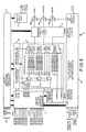
- FIG. 3 is a detailed block diagram of a RAMDAC.
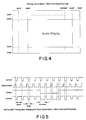
- Figure 4 shows timing generation for non-interlaced format.
- Figure 5 shows horizontal timing and composite sync generation for non-interlaced format.
- Figure 6 shows horizontal timing waveforms for interlaced format.
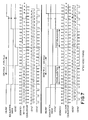
- Figure 7 shows NTSC video timing.
- FIG. 8 is a block overview diagram of the video timing generator of the present invention.
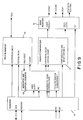
- FIG. 9 is a detailed block diagram of the video timing generator of the present invention.
- Figure 10 is a logic gate implementation of the video timing generator of the present invention.
- Figure 11 is a detailed block diagram showing the operation of equality comparators.
- Figure 12 shows field generator master mode timing.
- Figure 13 shows field generator slave mode timing.
- a system utilizing two or more video monitors displaying related or contiguous images generated by two or more computers may exhibit aberrations in the viewed images because the computers do not operate from a single timing reference.
- the present invention provides a simple, low cost technique for sharply reducing such aberrations in the viewed images.
- FIG. 2 represents a hypothetical arrangement having three systems; the number of systems may be increased or decreased without effect on the principle under discussion.
- Each of these systems includes a RAMDAC 21, a graphics engine, or other video data source such as rendering controller 14, a frame buffer memory 15 and host computer 12.
- Components other than the RAMDAC, are included as an example of an implementation of the RAMDAC in a complete system.
- VIEWER represents a person who observes the visual data presented on the three video displays.
- One key feature of this arrangement is the nature of the displayed video data.
- the data are related to one another, so that all three displays are required to represent a complete scene.
- the displayed data are not static, they convey the impression of movement.
- video display 2 provides the forward view from the simulator cockpit and video displays 1 and 3 provides the left and right views.
- Each of these displays may be stereoscopic displays, which impart a greater sense of "reality" to the simulation.
- each of the video displays must alternately and synchronously present left eye views and right eye views.
- the viewer wears special goggles which act as shutters for each eye, alternately and synchronously admitting left data to the left eye and right data to the right eye.
- buffers A and B Each of these buffers is connected to the graphics engine and to the RAMDAC.
- This double buffering scheme works in this way.
- the first view of an animated sequence is rendered into buffer A.
- the RAMDAC is told, by a control mechanism synchronized to the vertical blanking point of the video timing generator, to display data from buffer A.
- the CPU and the graphics engine begin rendering data for the next view into buffer B.
- the roles (rendering and display) of buffers A and B are again reversed. This process continues, resulting in the illusion of smooth motion (provided the rendering rate is sufficiently high) without noticeable aberrations.
- the point at which the buffer switching occurs is triggered by the completion of rendering and by the arrival of the subsequent video vertical blanking interval.
- the latter event is produced by the timing generator circuits of the RAMDAC and its external manifestation is a signal called the FIELD signal.
- a transition of the FIELD signal indicates that a new frame of video (a frame is one complete image) is about to start.
- the direction of the FIELD signal transition for non-interlace monoscopic displays, is irrelevant. However, the direction of the transition is very important for stereoscopic and interlaced displays.
- the level of the FIELD signal indicates which of the stereoscopic views, left or right, is to be processed and displayed by the RAMDAC, video display and stereoscopic goggles, if present.
- the level of the FIELD signal identifies the current field as either the odd field or the even field.
- the double buffered frame buffer is reorganized. Buffers A and B are retained but each one is again divided into two buffers. One of these holds data belonging to the left eye view and the other holds data belonging to the right eye view.
- the previously described rendering and display operations also apply in the stereoscopic mode.
- Figure 2 shows three systems which must display related or contiguous video data. Therefore, it is necessary for all systems to know when rendering of a particular video frame has been completed so that all systems can trigger the buffer switching operation at the same time.
- the time required for each system to complete its portion of the rendering task depends, in large part, on the contents of the scene being rendered. These contents will differ among the three systems. Consequently, the completion times will differ.
- Software and a local area network 17 are used to monitor the progress of rendering in the three systems. Once all systems have completed their rendering tasks, the buffer switching operation is triggered via the local area network. This facility solves one aspect of the synchronization problem. Another problem exists resulting from the fact that the timing references (clocks) or the three RAMDACs are independent of one another. Although the trigger for the buffer switching operation can be made to occur virtually simultaneously, the simultaneous transition of the three FIELD signals cannot be guaranteed by the described circuitry.
- Each of the three RAMDACs receives clock signals generated by three independent, crystal controlled oscillators (not shown in Figure 2) operating at a single nominal frequency.
- the actual frequencies produced by these oscillators will vary within a range of values (tolerance) which depends on the tolerance of the crystal resonator and local conditions such as temperature and, to some extent, voltage.
- tolerance which depends on the tolerance of the crystal resonator and local conditions such as temperature and, to some extent, voltage.
- two, or more, such oscillators will produce the same frequency over an extended period of time. For example, assume three such oscillators connected not to video displays but to three counter circuits used by three watches. If all three systems were to be turned on at the same instant and the clocks compared after a few hours of operation, the indicated times would be different and the differences would grow over time.
- the solution provided by the present invention does not seek to synchronize the three oscillators. Rather, it synchronizes events produced in the video timing generator circuits of the three RAMDACs (which are referenced to the oscillators). This approach exploits the fact that differences between the oscillators will be small if measured over a small interval of time.
- the period between successive FIELD signals is such a short interval (the period varies as a function of the particular video format, it is a maximum of 20 milliseconds and a minimum of about 13 milliseconds for the video formats supported in a typical implementation).
- system 1 is programmed to act as the master and systems 2 and 3 are programmed to act as slaves.
- the master system emits the FIELD signal and the slave systems receive it.
- system 1 becomes the source of the vertical interval timing reference and, in the stereoscopic mode, the controlling signal for stereoscopic goggles.
- the slaves respond to the received FIELD signal by resetting the counters (horizontal and vertical dimensions) which produce the video timing signals such as horizontal synch, vertical synch, and blanking.
- the reset state is defined to be identical to the state which exists in the master RAMDAC at the time when it emits the transition in the FIELD signal, thus achieving the required synchronization. If the three systems are observed, it would be discovered that vertical blanking (or start of frame) occurs nearly simultaneously.
- the differences in the times at which these events occur are caused by delays incurred in the interconnecting cables and in the moment at which the counters are actually reset. These differences are very small (on the order of microseconds) and cannot be perceived by the viewer.
- the present invention lies in this method of achieving synchronization and the circuit elements utilized.
- FIG. 3 which the components of a RAMDAC 21 which can be utilized to implement the present invention.
- the RAMDAC includes several functional blocks as follows: CPU port, interface logic, address pointers and data registers 31. pixel port, pixel input registers and serialization 33, shadow and RAM look-up tables, transfer control and overlay, underlay logic 35, color model selection 37, cursor logic serialization 39, monitor serial port 41, diagnostic registers and control logic 43, digital-analog converters (DAC) 45a-45c and PLL clock synthesizer, pixel clock divider and video timing generator 49.
- DAC digital-analog converters
- the invention lies mainly in an implementation of the video timing generator component of PLL clock synthesizer, pixel clock divider and video timing generator 49 which generates a FIELD signal for use by other RAMDACs as described above to provide synchronization. Therefore, the following description will be limited to the video timing generator, with information pertaining to the other components of the RAMDAC provided only as needed for an understanding of the present invention. Although the other components shown in Figure 3 may vary between RAMDACs of different manufacturers, persons skilled in the relevant art will recognize these various components and know how they or their equivalents may be implemented
- Frame buffer data is provided to the pixel port as pixel port signals such that the pixel inputs are divided into two ports, labeled A and B which consist of four groups per port. Furthermore, each group is divided into an upper byte and a lower byte. Thus, the pixel port comprises a total of 128 pixel bits contained in groups 0 through 7. Table 1 illustrates these assignments.
- the present invention utilizes a programmable timing generator, operating from a serial clock, and providing video display and video memory timing reference signals.
- the timing generator produces signals which are described below.
- the timing generator operates in two dimensions, specifically, horizontal, corresponding to the horizontal scan of a video display format, and vertical, corresponding to the vertical scan of a video display format.
- Events in the horizontal dimension such as horizontal synch, are placed on boundaries defined by the serial clock period.
- Events in the vertical dimension such as vertical sync, are placed on boundaries defined by a whole number of horizontal scans in the case of non-interlaced displays, or by half horizontal scans in the case of interlaced displays.
- the number of serial clock periods within a horizontal scan is variable and the number of horizontal scans within a video frame is variable.
- the design of the timing generator provides that when generator outputs are observed at the outputs of the RAMDAC, they are correctly placed relative to the video data being input to the pixel port. For example, if the generator is programmed to assert some event congruent to pixel number p, then it will be seen, at the RAMDAC output, to occur at a position corresponding to pixel number p.
- the timing generator incorporates a rudimentary frame synchronization feature as described below.
- the timing generator incorporates a timing generator control register having control register bit definitions which are shown in Table 2, "Timing Generator Control Register,” below. This register is read from and written to under control of host CPU 12 through the CPU port and interface logic which are coupled to multiplexed data/address bus D[07:00]. Table 2.
- CSYNC should look like the non-interlaced case: horizontal syncs occur on CSYNC except during vertical sync; during vertical sync CSYNC has serration pulses, (0) Equalize Enabled (1) Equalize Disabled 5 Master Mode R/W 0 This bit controls the direction of the FIELD I/O signal. When this bit is a logical zero, the RAMDAC uses the externally-provided FIELD signal to start at the top of a new frame. (0) Slave (1) Master 6 Interlaced Mode R/W 0 This field selects the mode of operation of the timing generator. A logical one causes the timing generator to operate in interlaced mode. (0) Non-Interlaced Mode (1) Interlaced Mode 7 Reserved
- the timing generator enables video frame synchronization of several displays.
- the timing generator is capable of operating either as a master or a slave as specified by bit 5 of the timing generator control register.
- the FIELD-signal is an output producing the periodic functions described in Table 3, "Timing Generator Signal Description,” below.
- the FIELD signal is an input which serves to set the horizontal and vertical elements of the generator so that they correspond to the start of vertical synch. Timing generators operated in the slave mode will not drive the FIELD signal. A further description of slave mode operation is described below.
- Video Enable (bit 0 of the timing generator control register) is forced to the disabled state by the assertion of system reset. This condition persists after the negation of system reset and stays in the disabled state until it is overwritten via the CPU port. Video Enable, when in the disabled state (i.e., reset), asserts composite blanking within the RAMDAC so that the video monitor remains black while the timing generator is being programmed to prevent random patterns or flashing from appearing on the display during, for example, a system boot when configuration and control data are being loaded into the timing generator.
- Timing Generator Enable Bit 1 of the timing generator control register
- This condition persists after the negation of system reset and stays in the disabled state until it is overwritten via the CPU Port.
- the purpose is to hold the timing generator in a known state while it is being programmed so that random FIELD, SC and SCen signals are not presented to other components of the system during such programming.
- system reset When asserted, system reset causes the timing generator to be in the slave mode.
- the FIELD signal is placed in a high impedance mode when the timing generator is in the slave mode.
- Timing Generator Signal Description Signal Name Description CSYNC* Composite Synch.
- This signal is conveyed to the video monitor as a discreet signal or, optionally, it is added to the Green channel DAC in the usual manner.
- the "synch on green” and other composite synch options are controlled by register programming.
- Composite Synch is the video synchronization signal and comprises horizontal and vertical, optionally serrated, synch components. For interlaced formats, such as NTSC and PAL, these components include horizontal equalization pulses.
- STSCAN A pixel port output. External circuitry interprets this signal as "start of each visible horizontal scan line" and uses it to index the video memory.
- FIELD A pixel port bidirectional signal.
- FIELD is an input when the synch generator is operated in the slave mode; it is an output when the generator is operated in the master mode. In interlaced formats, FIELD differentiates odd and even fields. In non-interlaced sequential display formats, FIELD simply indicates the start of the frame. External circuitry uses FIELD to index the video memory and to control LCD shutters used in stereographic viewing. FIELD changes state congruent to vertical synch. SCen* A pixel port output. Serial Clock enable is used by external circuitry to regulate the extraction of data from the serial port of the video memory. Assertion and negation of this signal are controlled by programmable registers in the horizontal SCen H Negation point, and SCen H Assertion point. SCen is active on unblanked lines as defined by VBlank Negation point and VBlank Assertion point.
- the timing generator is controlled by programming the appropriate values into the timing generator control registers. These registers are listed in Table 4, "Configuration Functions," below. Table 4 Configuration Functions Video Format Control Register PLL Control Register Transparent Overlay Mask Register Transparent Overlay Color Key Register Window Attribute - Active LUT Window Attribute - Shadow LUT Color LUT Timing Generator Control Register V-blank. Negation Point Register V-blank. Assertion Point Register V-sync. Negation Point Register V-sync. Assertion Point Register H-serration. Negation Point Register H-blank. Negation Point Register H-blank. Assertion Point Register H-sync. Negation Point Register H-sync. Negation Point Register H-sync.
- All horizontal register values are in units of the serial clock rate. All vertical register values are in units of the horizontal lines. In a typical embodiment, the values to load into the registers one less than the desired count or duration. The programming of these modes is described in the following paragraphs.
- the RAMDAC In addition to serrated sync support for interlaced mode, the RAMDAC also supports the generation of serrated sync for non-interlaced mode.
- the composite sync is derived by using horizontal sync outside of the vertical sync interval, and using the serrated sync waveform during vertical sync interval. This is graphically depicted in Figure 4, "Timing Generation-Non-Interlaced Format" with reference to the following description.
- the HSAP horizontal sync assertion point
- HSNP horizontal sync negation point
- HSERNP horizontal serration negation point
- the horizontal counter begins at a value of zero, with the HSYNC* and SERRATION* waveforms active (i.e. low). When the counter reaches the HSNP value, HSYNC* is deasserted on the next serial clock. The horizontal counter continues counting up until the programmed HSERNP value is reached, at which point the SERRATION* waveform is deasserted on the next serial clock. The horizontal counter continues until the HSAP value is reached, after which the horizontal counter will be restarted at zero on the next serial clock.
- FIG. 4 A diagram illustrating the relative register values related to active screen area is shown in Figure 4, "Timing Generation-Non-Interlaced Format.” Timing diagrams for the generation of composite sync are shown in Figure 5, "Horizontal Timing and Composite Sync Generation-Non-Interlaced Format.”
- HBLNK* is ten deasserted on the next serial clock, after the horizontal counter reaches the value programmed in the HBNP (Horizontal Blank Negation Point) register.
- the horizontal timing register values should satisfy the following relationships: 0 ⁇ HSNP ⁇ HBNP ⁇ HBAP ⁇ HSAP
- the VSYNC* vertical timing signal is generated using the values contained in the VSNP (Vertical Sync Negation Point) and VSAP (Vertical Sync Assertion Point) registers.
- the VBLANK* vertical timing signal is generated using the values contained in the VBAP (Vertical Blank Assertion Point) and VBNP (Vertical Blank Negation Point) registers. In non-interlaced mode, all vertical timing register intervals are specified in units of horizontal lines (i.e. the load period * HSAP).
- the vertical timing counter is incremented at each horizontal sync assertion time; subsequently, the only time that any vertical timing signals may transition is at HSYNC* assertion.
- the vertical timing registers should be programmed to satisfy the following relationship: 0 ⁇ VSNP ⁇ VBNP ⁇ VBAP ⁇ VSAP
- the composite blanking signal is derived by logically OR'ing HBLANK* with VBLANK*.
- timing events are based on half-line quantities.
- the HSYNC* and SERRATION* waveforms are generated in the same form as for non-interlaced mode; except that the HSYNC* and SERRATION* waveforms occur twice for each scan line. The contribution of these signals to the generation of the composite sync/video waveforms for interlaced mode is explained below.
- the HSYNC* and SERRATION* waveforms do not depend on scan line or the state of the FIELD signal; they are generated using only the contents of the horizontal counter. However, HBLANK* generation is also a function of the current FIELD and vertical scan line counter.
- the registers used for vertical events in interlaced mode are the VSAP (Vertical Sync Assertion Point), VSNP (Vertical Sync Negation Point), EIAP (Equalization Interval Assertion Point), EINP (Equalization Interval Negation Point), VBAP (Vertical Blank Assertion Point), and VBNP (Vertical Blank Negation Point).
- VSAP Vertical Sync Assertion Point
- VSNP Vertical Sync Negation Point
- EIAP Equalization Interval Assertion Point
- EINP Equalization Interval Negation Point
- VBAP Vertical Blank Assertion Point
- VBNP Vertical Blank Negation Point
- Some vertical timing signals depend only on the vertical counter value (VSYNC*, EQUALIZATION*); others also depend on the current field (VBLANK*, FIELD).
- the vertical counter is incremented at each leading edge of the internal HSYNC* signal; hence, all vertical timing registers must be programmed using half-line quantities (e.g. VSAP for NTSC has 525 half lines. For 525 half lines, VSAP is programmed as 524).
- the truth table for generating the vertical blanking signal is shown in Table 6, "Vertical Blank Generation-Interlaced Mode,” below.
- the vertical timing registers should satisfy the following relationship: 0 ⁇ VSNP ⁇ EINP ⁇ VBNP ⁇ VBAP ⁇ EIAP ⁇ VSAP
- Table 7 Composite Sync Generation-Interlaced Format
- HSYNC* and/or VSYNC* is disabled with the controls shown in Table 2, "Timing Generator Control Register,” the composite SYNC is as shown in Table 8, "Composite Sync Output when HSYNC* & VSYNC* Enabled/Disabled.”
- Table 8 Composite Sync Output when HSYNC* & VSYNC* Mode HSYNC* VSYNC* CSYNC output
- Non-interlaced enabled enabled Normal operation enabled disabled CSYNC* looks like HSYNC* (no serrations) disabled enabled CSYNC* looks like VSYNC* (no serrations) disabled disabled disabled CSYNC* inactive
- the RAMDAC provides the following timing generator outputs: SC*, SCen*, STSCAN, FIELD, and CSYNC*.
- the composite signal waveform is as previously described; the timing at the CSYNC* output pin is consistent with the analog DAC outputs.
- This output is an internally generated signal. This signal may be used by the memory controller of the host CPU to determine the proper row transfer address timing for the frame buffer serial port.
- the STSCAN logic will set the STSCAN at the falling edge of SCen if the next line is visible and reset the STSCAN at the rising edge of SCen.
- the SCen Serial clock enable
- the SCen is used for enabling the clocking of the serial data from the frame buffer memories.
- the assertion of SCen is controlled by programming the timing generator registers VBNP, VBAP, HSCenAP (Horizontal Serial Clock Enable Assertion Point), and HSCenNP (Horizontal Serial Clock Enable Negation Point).
- the timing generator accepts the FIELD signal as an input. In this mode, a transition occurring on this input will cause the vertical counter to be reset at the subsequent horizontal sync occurrence. If the RAMDAC is in interlaced mode, the level that the FIELD signal input transitions to will determine which field is current (i.e. a high-to-low transition causes the timing generator to start at the top of an even field on the next HSYNC* leading edge). Since the horizontal counters are not reset, eventually the clock drift will cause vertical sync for the slave to be one line longer, or the blanked front porch to be one line shorter.
- FIG 8 is a block overview diagram showing the signals input to and output from the video timing generator 50 of the present invention.
- the signals shown correspond to the signals with the same names described above with reference to Figure 3, excepting that Register Address is an address placed on D[07:00] and multiplexed with data placed on D[07:00],
- the video clock signal and the serial clock signal are produced by the PLL clock synthesizer and pixel clock divider components of digital-analog converters (DAC) 45a-45c and PLL clock synthesizer, pixel clock divider and video timing generator 49 shown in Figure 3 from a crystal oscillator input in a manner well known to those skilled in the art.
- the serial clock signal (SC*) is generated for the external clocking of the VRAM frame buffer and for the internal clocking of the video timing generator.
- Figure 8 depicts the interfaces connecting the video timing generator 50, the VRAM frame buffer 15a-15d and rendering controller 14.
- the purpose of this diagram is to show all of the paths taken by the FIELD signal.
- the connection to the rendering controller is provided to explain how the left and right eye video data are obtained from the frame buffer.
- the FIELD signal functions as a portion of the address which is passed to the frame buffer for copying video data from the its main memory into its serial shift registers. Video data are clocked out of these shift registers by the action of the serial clock, SC*, and the serial clock enable, SCen*, signals.
- the frame buffer memory When stereoscopic mode is active, the frame buffer memory is organized such that a single bit of address is sufficient to differentiate between memory locations containing left eye video data and those containing right eye video data.
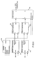
- FIG. 9 is a detailed block diagram showing the various functional blocks used to implement a video timing generator according to the present invention.
- the functional blocks are registers 51, horizontal and vertical counters 53, field generator 55, equality comparators 57 and event registers 59.
- the signals shown correspond to the signals with the same names described above with reference to Figure 3.
- Horizontal radix and vertical radix are set to the number of pixels on each scan line and the number of scan lines respectively for the video display connected to the RAMDAC. Vertical count is the current scan line and horizontal count is the current pixel on the current scan line.
- Event assertion and negation points are the values stored in registers 51 as shown in Table 3 and are loaded by the host CPU.
- Equality comparators 57 are a set of comparators which compare the horizontal and vertical counts to their respective radix values.
- field generator 55 generates the FIELD signal as follows.
- Equality comparator 61 receives the output of the vertical counter, V COUNT and the vertical radix, V RADIX. The former changes continuously, while the latter is a static value contained in a programmable register. The output of M1 is asserted when the two input values are equal in magnitude. V COUNT represents the number of the video line currently being processed. Consequently, the output of M1 will remain asserted for a period of time equal to that of one video scan line. It is necessary to process the output of M1 so that the resulting signal is referenced to the leading edge of M1 output assertion and is one video clock period in duration and is insensitive to the negation of the M1 output.
- flip-flop 63 (M5) will toggle as long as its clock enable input is asserted.
- the circuit comprised of flip-flop 65 (M2), flip-flop 67 (M3) and AND gate 69 (M4) operate as an edge discriminator which performs the task.
- the output of the edge discriminator (M4) is the clock enable input of flip-flop M5, whose output will toggle while clock enable is asserted. Because the clock enable signal is made to be one clock period in duration, the output of flip-flop M5 will change state once per video field.
- Tri-state driver 71 (M6) receives the output of flip-flop M5, and, if the master mode has been selected, drives the FIELD signal.
- the output of the edge discriminator M4 is also connected to the A input of the multiplexor 73 (M11).
- the multiplexor passes the output of the edge discriminator.
- the resulting signal is called FIELD RESET. It is used to reset the horizontal and vertical counters of the video timing generator.
- tri-state driver M6 enters the high impedance state and no longer drives the signal FIELD. Instead, the FIELD signal becomes an input to the field generator 55.
- the selection of the slave mode also causes the B input of multiplexor M11 to selected (in the master mode, the action of flip-flops M7, M8, M9 and gate M10 is of no importance).
- the (now) externally supplied FIELD signal is referenced to a clock (in another system) which operates at the same nominal frequency as the local clock.
- a clock in another system
- the phase relationships of the local clock to the external clock and the signals derived from these clocks can only be defined as variable. Therefore, it is necessary to guard against metastability.
- Flip-flops 75 and 77 are hardened against metastability and are used to synchronize the externally supplied FIELD signal to the local clock (such hardened flip-flops are commonly found in ASIC cell libraries).
- the FIELD signal is a square wave whose points of transition are congruent to vertical synch. Each transition point, therefore, corresponds to the point in time where V COUNT is equal to V RADIX. In order to reset the vertical and horizontal counters correctly, it is necessary to detect these transitions.
- Flip-flop 79 (M9) and XOR gate 81 (M10) form a transition detector which is insensitive to the direction of the transition producing an output pulse with a duration of one video clock period. Since slave mode has been selected, multiplexor M11 passes the output of gate M10 and drives the FIELD RESET signal.
- FIG. 11 represents the comparisons performed to generate a particular timing signal of the video timing generator.
- Counter 53a is loaded with the radix of the timing signal.
- Counter 53a increments each video clock and the count is provided to comparators 57a and 57b.
- the comparators 57a and 57b compare the current count with the assertion point value and negation point value previously loaded in registers 51a and 51b respectively.
- the comparators toggle event register 59a, which is a JK flip-flop, based on the comparison results, and the output of the flip-flop provides the particular timing signal.
- Figure 12 shows the timing of the signals produced within field generator 55 for master mode timing.
- Figure 13 shows the timing of the signals produced within field generator 55 for slave mode timing.
Landscapes
- Engineering & Computer Science (AREA)
- Multimedia (AREA)
- Theoretical Computer Science (AREA)
- Physics & Mathematics (AREA)
- General Physics & Mathematics (AREA)
- Computer Hardware Design (AREA)
- Signal Processing (AREA)
- Human Computer Interaction (AREA)
- General Engineering & Computer Science (AREA)
- Controls And Circuits For Display Device (AREA)
- Digital Computer Display Output (AREA)
- Television Signal Processing For Recording (AREA)
Applications Claiming Priority (2)
| Application Number | Priority Date | Filing Date | Title |
|---|---|---|---|
| US40826895A | 1995-03-21 | 1995-03-21 | |
| US408268 | 1995-03-21 |
Publications (2)
| Publication Number | Publication Date |
|---|---|
| EP0734011A2 true EP0734011A2 (fr) | 1996-09-25 |
| EP0734011A3 EP0734011A3 (fr) | 1999-01-20 |
Family
ID=23615575
Family Applications (1)
| Application Number | Title | Priority Date | Filing Date |
|---|---|---|---|
| EP96301747A Withdrawn EP0734011A3 (fr) | 1995-03-21 | 1996-03-14 | Synchronisation d'une zone de trames indépendantes |
Country Status (3)
| Country | Link |
|---|---|
| US (1) | US5963200A (fr) |
| EP (1) | EP0734011A3 (fr) |
| JP (1) | JP3795569B2 (fr) |
Cited By (7)
| Publication number | Priority date | Publication date | Assignee | Title |
|---|---|---|---|---|
| WO1998032068A1 (fr) * | 1997-01-17 | 1998-07-23 | Intergraph Corporation | Dispositif et procede de synchronisation pour affichage multiple |
| GB2326573A (en) * | 1997-06-03 | 1998-12-23 | Hewlett Packard Co | Method and apparatus for synchronising vertical refresh and dispaly of left versus right channels in a stereoscopic multi-display computer graphics system. |
| US6157395A (en) * | 1997-05-19 | 2000-12-05 | Hewlett-Packard Company | Synchronization of frame buffer swapping in multi-pipeline computer graphics display systems |
| WO2000078037A3 (fr) * | 1999-06-10 | 2001-04-26 | Enseo Inc | Systeme et procede de synchronisation, de stockage et de reproduction fidele de signaux video |
| DE10044032A1 (de) * | 2000-09-06 | 2002-03-14 | Deutsche Telekom Ag | 3-D Sehen |
| EP2323029A2 (fr) * | 1999-06-15 | 2011-05-18 | ATI Technologies ULC | Méthode et dispositif de rendu d'images vidéo |
| CN103886849A (zh) * | 2009-12-30 | 2014-06-25 | 英特尔公司 | 用于对齐帧数据的技术 |
Families Citing this family (63)
| Publication number | Priority date | Publication date | Assignee | Title |
|---|---|---|---|---|
| CN1035878C (zh) * | 1992-02-18 | 1997-09-17 | 万有制药株式会社 | 吲哚并吡咯并咔唑衍生物 |
| US5804564A (en) * | 1994-05-09 | 1998-09-08 | Banyu Pharmaceutical Co., Ltd. | Antitumor indolopyrrolocarbazole derivatives |
| US6041345A (en) * | 1996-03-08 | 2000-03-21 | Microsoft Corporation | Active stream format for holding multiple media streams |
| US6181300B1 (en) * | 1998-09-09 | 2001-01-30 | Ati Technologies | Display format conversion circuit with resynchronization of multiple display screens |
| US6819305B2 (en) * | 1999-01-28 | 2004-11-16 | Conexant Systems, Inc. | Method and apparatus for detection of a video display device |
| US6754234B1 (en) * | 1999-05-21 | 2004-06-22 | Ati International Srl | Method and apparatus for asynchronous frame synchronization |
| US6529175B2 (en) * | 2000-01-27 | 2003-03-04 | Vrex, Inc. | Stereoscopic LCD shutter glass driver system |
| US6864900B2 (en) * | 2001-05-18 | 2005-03-08 | Sun Microsystems, Inc. | Panning while displaying a portion of the frame buffer image |
| US7061540B2 (en) * | 2001-12-19 | 2006-06-13 | Texas Instruments Incorporated | Programmable display timing generator |
| US6784881B2 (en) | 2002-01-04 | 2004-08-31 | Sun Microsystems, Inc. | Synchronizing multiple display channels |
| US6700580B2 (en) * | 2002-03-01 | 2004-03-02 | Hewlett-Packard Development Company, L.P. | System and method utilizing multiple pipelines to render graphical data |
| US6727904B2 (en) * | 2002-03-01 | 2004-04-27 | Hewlett-Packard Development Company, L.P. | System and method for rendering graphical data |
| US6894692B2 (en) * | 2002-06-11 | 2005-05-17 | Hewlett-Packard Development Company, L.P. | System and method for sychronizing video data streams |
| US7668099B2 (en) * | 2003-06-13 | 2010-02-23 | Apple Inc. | Synthesis of vertical blanking signal |
| US7161570B2 (en) * | 2003-08-19 | 2007-01-09 | Brillian Corporation | Display driver architecture for a liquid crystal display and method therefore |
| KR101022472B1 (ko) * | 2004-01-17 | 2011-03-16 | 삼성전자주식회사 | 효율적으로 버스를 사용하는 방법 |
| EP1929849A4 (fr) * | 2005-05-05 | 2011-01-05 | Reddy Degapudi Janardhana | Ordinateur portable avec un affichage dos a dos |
| EP1752856B1 (fr) * | 2005-08-11 | 2008-06-25 | St Microelectronics S.A. | Générateur de signal de forme d'onde modifiable |
| US20070097016A1 (en) * | 2005-10-27 | 2007-05-03 | Scott McGowan | Triple Screen Video Arcade Circuit |
| US8872754B2 (en) * | 2006-03-29 | 2014-10-28 | Nvidia Corporation | System, method, and computer program product for controlling stereo glasses shutters |
| US8169467B2 (en) * | 2006-03-29 | 2012-05-01 | Nvidia Corporation | System, method, and computer program product for increasing an LCD display vertical blanking interval |
| US7948450B2 (en) * | 2006-11-09 | 2011-05-24 | D3 Led, Llc | Apparatus and method for allowing display modules to communicate information about themselves to other display modules in the same display panel |
| US8872896B1 (en) * | 2007-04-09 | 2014-10-28 | Nvidia Corporation | Hardware-based system, method, and computer program product for synchronizing stereo signals |
| JP5198818B2 (ja) * | 2007-09-10 | 2013-05-15 | ラピスセミコンダクタ株式会社 | 同期処理システム及び半導体集積回路 |
| US8139072B2 (en) * | 2008-04-14 | 2012-03-20 | Mcgowan Scott James | Network hardware graphics adapter compression |
| US9122443B1 (en) | 2008-05-01 | 2015-09-01 | Rockwell Collins, Inc. | System and method for synchronizing multiple video streams |
| US8300056B2 (en) | 2008-10-13 | 2012-10-30 | Apple Inc. | Seamless display migration |
| US9165493B2 (en) | 2008-10-14 | 2015-10-20 | Apple Inc. | Color correction of electronic displays utilizing gain control |
| US9063713B2 (en) * | 2008-10-28 | 2015-06-23 | Apple Inc. | Graphics controllers with increased thermal management granularity |
| US20100164966A1 (en) * | 2008-12-31 | 2010-07-01 | Apple Inc. | Timing controller for graphics system |
| US8207974B2 (en) * | 2008-12-31 | 2012-06-26 | Apple Inc. | Switch for graphics processing units |
| US8508538B2 (en) * | 2008-12-31 | 2013-08-13 | Apple Inc. | Timing controller capable of switching between graphics processing units |
| US9542914B2 (en) * | 2008-12-31 | 2017-01-10 | Apple Inc. | Display system with improved graphics abilities while switching graphics processing units |
| US9075559B2 (en) * | 2009-02-27 | 2015-07-07 | Nvidia Corporation | Multiple graphics processing unit system and method |
| US9135675B2 (en) * | 2009-06-15 | 2015-09-15 | Nvidia Corporation | Multiple graphics processing unit display synchronization system and method |
| US20110043514A1 (en) * | 2009-08-24 | 2011-02-24 | ATI Technologies ULC. | Method and apparatus for multiple display synchronization |
| US20110149052A1 (en) * | 2009-12-22 | 2011-06-23 | Samsung Electronics Co., Ltd. | 3d image synchronization apparatus and 3d image providing system |
| US8643658B2 (en) * | 2009-12-30 | 2014-02-04 | Intel Corporation | Techniques for aligning frame data |
| US20110164118A1 (en) * | 2010-01-06 | 2011-07-07 | Samsung Electronics Co., Ltd. | Display apparatuses synchronized by one synchronization signal |
| US8648868B2 (en) | 2010-01-06 | 2014-02-11 | Apple Inc. | Color correction to facilitate switching between graphics-processing units |
| US8797334B2 (en) | 2010-01-06 | 2014-08-05 | Apple Inc. | Facilitating efficient switching between graphics-processing units |
| US8368702B2 (en) | 2010-01-06 | 2013-02-05 | Apple Inc. | Policy-based switching between graphics-processing units |
| US8874981B2 (en) | 2010-05-12 | 2014-10-28 | Mediatek Inc. | Method of creating target storage layout table referenced for partitioning storage space of storage device and related electronic device and machine-readable medium |
| US9113136B2 (en) * | 2010-07-15 | 2015-08-18 | Mediatek Singapore Pte. Ltd. | Video processing apparatus and method for simultaneously displaying a plurality of video signals on display device |
| US20120033036A1 (en) * | 2010-08-04 | 2012-02-09 | Disney Enterprises, Inc. | System and method for displaying three-dimensional video |
| US9094678B1 (en) | 2010-09-29 | 2015-07-28 | Nvidia Corporation | System, method, and computer program product for inverting a polarity of each cell of a display device |
| US9094676B1 (en) | 2010-09-29 | 2015-07-28 | Nvidia Corporation | System, method, and computer program product for applying a setting based on a determined phase of a frame |
| US8933944B2 (en) | 2010-10-13 | 2015-01-13 | Boston Scientific Neuromodulation Corporation | External controller for an implantable medical device with dual microcontrollers for improved graphics rendering |
| US8866825B2 (en) | 2010-12-15 | 2014-10-21 | Ati Technologies Ulc | Multiple display frame rendering method and apparatus |
| US20120169852A1 (en) * | 2011-01-04 | 2012-07-05 | Samsung Electronics Co., Ltd. | Display apparatus and system |
| US9164288B2 (en) | 2012-04-11 | 2015-10-20 | Nvidia Corporation | System, method, and computer program product for presenting stereoscopic display content for viewing with passive stereoscopic glasses |
| EP2864866A2 (fr) * | 2012-06-22 | 2015-04-29 | Universität des Saarlandes | Procédé et système pour afficher des pixels sur des dispositifs d'affichage |
| CN103067729A (zh) * | 2013-01-31 | 2013-04-24 | 利亚德光电股份有限公司 | 拼接屏体立体显示的同步信号处理方法及装置、拼接屏体 |
| US9818379B2 (en) | 2013-08-08 | 2017-11-14 | Nvidia Corporation | Pixel data transmission over multiple pixel interfaces |
| EP2854024A1 (fr) * | 2013-09-27 | 2015-04-01 | Siemens Aktiengesellschaft | Panneau d'affichage conçu pour être utilisé dans des dispositifs d'interface homme-machine |
| JP6516480B2 (ja) | 2015-01-19 | 2019-05-22 | キヤノン株式会社 | 表示装置、表示システム及び表示方法 |
| JP6208732B2 (ja) * | 2015-11-13 | 2017-10-04 | 株式会社Pfu | 映像処理装置、映像処理システム、および、映像処理方法 |
| JP6500199B2 (ja) * | 2017-01-13 | 2019-04-17 | 株式会社アクセル | 画像処理装置、および画像処理システム |
| JP6500198B2 (ja) * | 2017-01-13 | 2019-04-17 | 株式会社アクセル | 遊技機 |
| FR3062495B1 (fr) * | 2017-02-01 | 2020-12-25 | Peugeot Citroen Automobiles Sa | Dispositif d’analyse de la synchronisation d’images sur des voies d’affichage distinctes |
| US10719286B2 (en) * | 2018-03-29 | 2020-07-21 | Microsoft Technology Licensing, Llc | Mechanism to present in an atomic manner a single buffer that covers multiple displays |
| US10789911B2 (en) * | 2018-12-11 | 2020-09-29 | Microsoft Technology Licensing, Llc | Phase locked multi-display synchronization |
| US11430410B2 (en) * | 2020-06-01 | 2022-08-30 | Ati Technologies Ulc | Display cycle control system |
Family Cites Families (12)
| Publication number | Priority date | Publication date | Assignee | Title |
|---|---|---|---|---|
| US4498098A (en) * | 1982-06-02 | 1985-02-05 | Digital Equipment Corporation | Apparatus for combining a video signal with graphics and text from a computer |
| JPH0640256B2 (ja) * | 1983-12-26 | 1994-05-25 | 株式会社日立製作所 | 表示制御装置 |
| US5281957A (en) * | 1984-11-14 | 1994-01-25 | Schoolman Scientific Corp. | Portable computer and head mounted display |
| GB2175471A (en) * | 1985-05-09 | 1986-11-26 | Visage Inc | Synchronizing video sources |
| US4860251A (en) * | 1986-11-17 | 1989-08-22 | Sun Microsystems, Inc. | Vertical blanking status flag indicator system |
| US5021775A (en) * | 1989-02-27 | 1991-06-04 | Motorola, Inc. | Synchronization method and circuit for display drivers |
| JPH03105385A (ja) * | 1989-09-20 | 1991-05-02 | Hitachi Ltd | 表示制御装置 |
| US5124804A (en) * | 1990-09-10 | 1992-06-23 | Ncr Corporation | Programmable resolution video controller |
| DE69223428T2 (de) * | 1991-02-04 | 1998-06-04 | Koninkl Philips Electronics Nv | Datenkommunikationssystem auf einer Serienbusbasis und Überwachungsstation zur Verwendung mit einem derartigen System |
| US5394171A (en) * | 1992-11-02 | 1995-02-28 | Zenith Electronics Corp. | Synchronizing signal front end processor for video monitor |
| US5523886A (en) * | 1994-01-04 | 1996-06-04 | Sega Of America, Inc. | Stereoscopic/monoscopic video display system |
| US5500819A (en) * | 1994-09-30 | 1996-03-19 | Cirrus Logic, Inc. | Circuits, systems and methods for improving page accesses and block transfers in a memory system |
-
1996
- 1996-03-14 EP EP96301747A patent/EP0734011A3/fr not_active Withdrawn
- 1996-03-21 JP JP08992296A patent/JP3795569B2/ja not_active Expired - Lifetime
-
1997
- 1997-08-20 US US08/914,973 patent/US5963200A/en not_active Expired - Lifetime
Cited By (15)
| Publication number | Priority date | Publication date | Assignee | Title |
|---|---|---|---|---|
| US6046709A (en) * | 1997-01-17 | 2000-04-04 | Intergraph Corporation | Multiple display synchronization apparatus and method |
| WO1998032068A1 (fr) * | 1997-01-17 | 1998-07-23 | Intergraph Corporation | Dispositif et procede de synchronisation pour affichage multiple |
| US6157395A (en) * | 1997-05-19 | 2000-12-05 | Hewlett-Packard Company | Synchronization of frame buffer swapping in multi-pipeline computer graphics display systems |
| GB2326573B (en) * | 1997-06-03 | 2002-04-03 | Hewlett Packard Co | Synchronization of left/right channel display and vertical refresh in multi-display stereoscopic computer graphics systems |
| GB2326573A (en) * | 1997-06-03 | 1998-12-23 | Hewlett Packard Co | Method and apparatus for synchronising vertical refresh and dispaly of left versus right channels in a stereoscopic multi-display computer graphics system. |
| US6122000A (en) * | 1997-06-03 | 2000-09-19 | Hewlett Packard Company | Synchronization of left/right channel display and vertical refresh in multi-display stereoscopic computer graphics systems |
| DE19810062C2 (de) * | 1997-06-03 | 2002-05-29 | Hewlett Packard Co | Synchronisation einer links/rechts-Kanalanzeige und vertikale Auffrischung in stereoskopischen Mehranzeigencomputergraphiksystemen |
| US6606127B1 (en) | 1999-06-10 | 2003-08-12 | Enseo, Inc. | System and method for synchronizing, storing and accurately reproducing video signals |
| WO2000078037A3 (fr) * | 1999-06-10 | 2001-04-26 | Enseo Inc | Systeme et procede de synchronisation, de stockage et de reproduction fidele de signaux video |
| EP2323029A2 (fr) * | 1999-06-15 | 2011-05-18 | ATI Technologies ULC | Méthode et dispositif de rendu d'images vidéo |
| DE10044032A1 (de) * | 2000-09-06 | 2002-03-14 | Deutsche Telekom Ag | 3-D Sehen |
| US7411604B2 (en) | 2000-09-06 | 2008-08-12 | Deutsche Telekom Ag | Synchronization of a stereoscopic camera |
| CN103886849A (zh) * | 2009-12-30 | 2014-06-25 | 英特尔公司 | 用于对齐帧数据的技术 |
| CN106251825A (zh) * | 2009-12-30 | 2016-12-21 | 英特尔公司 | 用于对齐帧数据的技术 |
| CN103886849B (zh) * | 2009-12-30 | 2017-01-04 | 英特尔公司 | 用于对齐帧数据的方法和设备 |
Also Published As
| Publication number | Publication date |
|---|---|
| US5963200A (en) | 1999-10-05 |
| EP0734011A3 (fr) | 1999-01-20 |
| JPH09120277A (ja) | 1997-05-06 |
| JP3795569B2 (ja) | 2006-07-12 |
Similar Documents
| Publication | Publication Date | Title |
|---|---|---|
| US5963200A (en) | Video frame synchronization of independent timing generators for frame buffers in a master-slave configuration | |
| US8384707B2 (en) | Method for synchronizing display of images in a multi-display computer system | |
| EP0492795B1 (fr) | Système multimédia | |
| US4450442A (en) | Display processor for superimposed-picture display system | |
| EP0493881B1 (fr) | Architecture de bus pour un système multimédia | |
| EP0493882B1 (fr) | Circuit interface de bus pour un système multimédia | |
| US6122000A (en) | Synchronization of left/right channel display and vertical refresh in multi-display stereoscopic computer graphics systems | |
| CA2055296C (fr) | Circuit de traitement de signaux d'imagerie analogiques pour systeme multimedia | |
| US5929924A (en) | Portable PC simultaneously displaying on a flat-panel display and on an external NTSC/PAL TV using line buffer with variable horizontal-line rate during vertical blanking period | |
| US6535208B1 (en) | Method and apparatus for locking a plurality of display synchronization signals | |
| JP3419046B2 (ja) | 映像表示装置 | |
| US7289539B1 (en) | Synchronization of stereo glasses in multiple-end-view environments | |
| JPH10319928A (ja) | フォーマット変換用マルチスキャンビデオタイミング発生器 | |
| JP3451722B2 (ja) | 映像データ転送装置 | |
| CA2055037C (fr) | Circuit d'arbitrage pour systeme multimedia | |
| EP0125768A2 (fr) | Méthode et appareil pour la génération de signaux d'horloge digitale à phase rigide | |
| EP0770982A2 (fr) | Dispositif d'étalonnage et de fusionnement pour des adapteurs graphiques vidéo | |
| EP0490505B1 (fr) | Module de commande de média pour un système multimédia | |
| JPS6153880A (ja) | 文字画像表示制御装置 | |
| KR100266164B1 (ko) | 분할된 화면 동기 구현 방법 및 장치(Method for Emboding Sync of Divided Picture and Apparatus thereof) | |
| KR930005808B1 (ko) | 화상 시스템 | |
| GB2368995A (en) | Synchronising vertical refresh cycles of first and second display systems | |
| JP2003280626A (ja) | 画像合成装置 | |
| Macourek | Programmable Mixing of Color Graphics and External Video Using New Lsi Display Processor | |
| JPH11126060A (ja) | キャラクタ表示装置 |
Legal Events
| Date | Code | Title | Description |
|---|---|---|---|
| PUAI | Public reference made under article 153(3) epc to a published international application that has entered the european phase |
Free format text: ORIGINAL CODE: 0009012 |
|
| AK | Designated contracting states |
Kind code of ref document: A2 Designated state(s): DE FR GB NL SE |
|
| PUAL | Search report despatched |
Free format text: ORIGINAL CODE: 0009013 |
|
| RHK1 | Main classification (correction) |
Ipc: G06F 3/14 |
|
| AK | Designated contracting states |
Kind code of ref document: A3 Designated state(s): DE FR GB NL SE |
|
| 17P | Request for examination filed |
Effective date: 19990628 |
|
| GRAP | Despatch of communication of intention to grant a patent |
Free format text: ORIGINAL CODE: EPIDOSNIGR1 |
|
| STAA | Information on the status of an ep patent application or granted ep patent |
Free format text: STATUS: THE APPLICATION IS DEEMED TO BE WITHDRAWN |
|
| 18D | Application deemed to be withdrawn |
Effective date: 20050714 |