EP0735580A1 - Verfahren zur Herstellung von Isolationsgraben - Google Patents
Verfahren zur Herstellung von Isolationsgraben Download PDFInfo
- Publication number
- EP0735580A1 EP0735580A1 EP95830125A EP95830125A EP0735580A1 EP 0735580 A1 EP0735580 A1 EP 0735580A1 EP 95830125 A EP95830125 A EP 95830125A EP 95830125 A EP95830125 A EP 95830125A EP 0735580 A1 EP0735580 A1 EP 0735580A1
- Authority
- EP
- European Patent Office
- Prior art keywords
- silicon
- dielectric
- layer
- process according
- isolation region
- Prior art date
- Legal status (The legal status is an assumption and is not a legal conclusion. Google has not performed a legal analysis and makes no representation as to the accuracy of the status listed.)
- Granted
Links
Images


Classifications
-
- H—ELECTRICITY
- H10—SEMICONDUCTOR DEVICES; ELECTRIC SOLID-STATE DEVICES NOT OTHERWISE PROVIDED FOR
- H10W—GENERIC PACKAGES, INTERCONNECTIONS, CONNECTORS OR OTHER CONSTRUCTIONAL DETAILS OF DEVICES COVERED BY CLASS H10
- H10W10/00—Isolation regions in semiconductor bodies between components of integrated devices
- H10W10/01—Manufacture or treatment
- H10W10/011—Manufacture or treatment of isolation regions comprising dielectric materials
- H10W10/014—Manufacture or treatment of isolation regions comprising dielectric materials using trench refilling with dielectric materials, e.g. shallow trench isolations
- H10W10/0145—Manufacture or treatment of isolation regions comprising dielectric materials using trench refilling with dielectric materials, e.g. shallow trench isolations of trenches having shapes other than rectangular or V-shape
-
- H—ELECTRICITY
- H10—SEMICONDUCTOR DEVICES; ELECTRIC SOLID-STATE DEVICES NOT OTHERWISE PROVIDED FOR
- H10W—GENERIC PACKAGES, INTERCONNECTIONS, CONNECTORS OR OTHER CONSTRUCTIONAL DETAILS OF DEVICES COVERED BY CLASS H10
- H10W10/00—Isolation regions in semiconductor bodies between components of integrated devices
- H10W10/01—Manufacture or treatment
- H10W10/041—Manufacture or treatment of isolation regions comprising polycrystalline semiconductor materials
-
- H—ELECTRICITY
- H10—SEMICONDUCTOR DEVICES; ELECTRIC SOLID-STATE DEVICES NOT OTHERWISE PROVIDED FOR
- H10W—GENERIC PACKAGES, INTERCONNECTIONS, CONNECTORS OR OTHER CONSTRUCTIONAL DETAILS OF DEVICES COVERED BY CLASS H10
- H10W10/00—Isolation regions in semiconductor bodies between components of integrated devices
- H10W10/10—Isolation regions comprising dielectric materials
- H10W10/17—Isolation regions comprising dielectric materials formed using trench refilling with dielectric materials, e.g. shallow trench isolations
-
- H—ELECTRICITY
- H10—SEMICONDUCTOR DEVICES; ELECTRIC SOLID-STATE DEVICES NOT OTHERWISE PROVIDED FOR
- H10W—GENERIC PACKAGES, INTERCONNECTIONS, CONNECTORS OR OTHER CONSTRUCTIONAL DETAILS OF DEVICES COVERED BY CLASS H10
- H10W10/00—Isolation regions in semiconductor bodies between components of integrated devices
- H10W10/40—Isolation regions comprising polycrystalline semiconductor materials
Definitions
- the present invention relates to a process for forming, on a semiconductor substrate, a dielectric isolation structure between two zones of an integrated circuit wherein active regions of electronic components have already been defined.
- the invention relates, in particular but not solely, to electronic devices having a driver circuit and one or more power transistors integrated monolithically thereto, and concerns the formation of a trench isolation structure. Reference will be made hereinafter to this specific application for convenience of illustration.
- Figure 1a shows a circuit including a single low-voltage driver transistor of the npn type and single power transistor, also of the npn type.
- This known structure uses a diffused zone 4 of the n type, called the junction isolation zone, which separates regions 30 and 31 of the p type to isolate the power stage from the driver circuit.
- this solution has a drawback in that it is limiting of the breakdown voltage for the resultant components due to inherent features of the method used, which provides for different concentrations of the various dopants.
- DTI Deep Trench Isolation
- the trench should be estended through the n-type epitaxial layer, approximately 1 micron thick.
- the depth attained by the isolation does not exceed 5 microns.
- the trench width should not exceed 2 microns, for otherwise, very thick layers of polycrystalline silicon, or polySi, would have to be deposited, resulting in decreased productivity and increased cost of the process.
- the trench depth should be increased, because the epitaxial layers to be etched are thicker, being on the order of 15 to 25 microns thick; on the other hand, trenches with higher aspect ratii (ratio of trench depth to width) than 10 are difficult to make.
- the underlying technical problem of the present invention is to provide a method of making a structure for isolating two zones of an integrated circuit, which can overcome the aforementioned limitations and/or drawbacks of prior art methods.
- the technical problem is solved by a process for forming, on a semiconductor substrate, a dielectric isolation structure between two zones of an integrated circuit where active regions of electronic components have been previously defined, which process is as outlined above and characterized in that it comprises the following steps of:
- the invention provides for the isolation structure to be formed after the formation of the active zones of the components.
- this sequential processing scheme allows the stresses built into the silicon, on account of the materials which enter the making of the isolation by high-temperature processes having different coefficients of thermal expansion, to be minimized.
- Table 1 of Reference (3) can be altered by the addition of the following column to encompass information about our own solution, namely: etch equipment wet etch chemistry KOH etch rate >1 micron/minute throughput/cost (wafer/hour/$) 100 wafers/hr/30K$ si ox selectivity 50:1 trench shape isotropic comments easily deeper than 25 microns or wet etch using KOH (potassium hydroxide), an etch rate of one micron per minute, and an hourly capacity of more than one hundred slices.
- KOH potassium hydroxide
- the method of this invention allows isolation regions to be formed to a depth of upwards of 25 microns.
- This value is essential to the operation of circuits which contain one or more power transistors and a driver circuit operated at higher voltages than a few tens Volts.
- Figure 1 shows an embodiment of a device with a junction type of isolation according to the prior art.
- Figure 1b shows an embodiment of a device with a dielectric type of isolation according to the prior art.
- FIGS 2a to 2d show successive steps in the making of the dielectric isolation structure according to the invention.
- Figures 3a and 3b show successive steps in the making of a modified embodiment of the dielectric isolation structure according to the invention.
- FIGS 4a to 4c show successive steps in the making of another modified embodiment of the dielectric isolation structure according to the invention.
- Figure 5 shows a further modified embodiment of the inventive isolation structure.
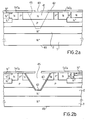
- Figure 2a is a vertical section view, enlarged but out of scale, of a semiconductor electronic device which has been formed with the active regions and an opening 40, through the oxide 42 provided on the device surface, within the region where the dielectric isolation structure 45 is to be formed.
- Figure 2b is a view showing schematically the same device as in Figure 2a, after the steps of wet etching the silicon underlying the oxide 41 by means of potassium hydroxide, KOH, and then growing the thermal oxide 43 have been completed.
- Figure 2c is a schematic view of the device shown in Figure 2b, having a layer of polycrystalline silicon, or polySi, 46 deposited thereon whose thickness is approximately one half the size of the opening 40 formed through the oxide 42.
- Figure 2d is a schematic view of the device shown in Figure 2c after the polySi 46 oxidation step.
- the silicon 41 area not covered with silicon oxide 42 is then etched to produce a trench which extends down to the epitaxial layer 2 of N - type in contact with the substrate 1 of N + type.
- the etching can be performed using a wet solution of potassium hydroxide (KOH) or by plasma etching.
- KOH potassium hydroxide
- HNO 3 hydrofluoric acid and nitric acid
- Thermal oxide 43 is also grown on the bottom of the trench 45.
- the process sequence includes, at this point, the deposition of a polySi layer 46.
- amorphous silicon could be deposited.
- the thickness of this layer is preferably equal to one half the spacing between the two portions of the oxide 42 which are present on the device surface, i.e. one half the size of the opening 40.
- the deposition is a conforming one, that is, the layer is grown evenly in a manner unaffected by topography, the portions of the polySi 46 grown on either sides of the isolation region 42, will merge together at the surface, as shown in Figure 2c, until they cover the opening 40.
- any increase in the thickness of the polySi 47 within the trench will be disallowed, and further depositions of polySi can only lead to surfacial increase of the layer 46 thickness. Since the polySi deposition is carried out at low pressures of a few mTorrs, under controlled atmosphere, no air can be trapped inside the trench. Thus, a potentially dangerous condition is avoided where the structure is to undergo subsequent thermal processing at a high temperature.
- a metallization of the underside 49 of the substrate is also contemplated for contacting the collector of the power transistor Cp, as shown in Figure 1a.
- the oxidation also occurs within the trench, whose walls 51 become covered with a fairly thick oxide layer 53, as shown in Figure 3b. It is preferable, in this case, that the resultant structure be subjected to no subsequent processing at higher temperatures than that used for the oxidation step.
- An advantage of the embodiment shown in Figures 3a and 3b is that no polySi is present on the interior walls of the trench, which are in addition covered with a fairly thick oxide layer.
- a thin layer of silicon nitride (Si 3 N 4 ) 54 may be deposited on which the polySi 55 will then be deposited.
- the trench can be planarized without resorting to any deposition and oxidation of polySi.
- Conforming layers of deposited oxide such as TEOS (tetra-ortho-siloxane), or unconforming layers such as the well-known PSG, BPSG, SOG can be used to produce the isolating layer which will subsequently allow metallization paths to be established for connecting the various active components.
- TEOS tetra-ortho-siloxane
- unconforming layers such as the well-known PSG, BPSG, SOG
- the trench can also be planarized using organic materials, such as polyimide, and etch-back processes with or without a photoresist, as are well known to the skilled ones.
- organic materials such as polyimide, and etch-back processes with or without a photoresist, as are well known to the skilled ones.
- the structure be subjected to no thermal treatments at temperatures above the curing temperature of the polyimide, to prevent degradation of the latter.
- the structure of this invention mainly distinguishes itself from the prior art structures by that it utilizes the two portions of surface oxide for the subsequent planarization step.
- the device dimensions are such that the size of the isolation zone can be regarded as negligible.
- no definition of trenches with near-vertical walls, having high aspect ratii and no recesses, is required, and the presence of two "projecting" oxide portions from the silicon etching step is utilized instead as the start point for the dielectric deposition.
- the trench walls have been intentionally drawn at an angle of about 55 degrees from the normal to the surface, just as would be the case if an aqueous solution of potassium hydroxide (KOH) is used for etching the silicon.
- KOH potassium hydroxide
- the trench is defined subsequently to forming the active regions, that is after the heaviest thermal cycles have been completed. Accordingly, the active zones of the components have already been formed and the only steps left to complete the device processing are the definition of the contact area and the metallization and passivation steps.
Landscapes
- Element Separation (AREA)
- Bipolar Transistors (AREA)
- Metal-Oxide And Bipolar Metal-Oxide Semiconductor Integrated Circuits (AREA)
- Bipolar Integrated Circuits (AREA)
Priority Applications (5)
| Application Number | Priority Date | Filing Date | Title |
|---|---|---|---|
| DE69533773T DE69533773D1 (de) | 1995-03-31 | 1995-03-31 | Verfahren zur Herstellung von Isolationsgraben |
| EP95830125A EP0735580B1 (de) | 1995-03-31 | 1995-03-31 | Verfahren zur Herstellung von Isolationsgraben |
| JP8076908A JPH08279554A (ja) | 1995-03-31 | 1996-03-29 | 誘電体分離構造の形成方法 |
| US08/625,875 US6001705A (en) | 1995-03-31 | 1996-04-01 | Process for realizing trench structures |
| US09/431,714 US6362072B1 (en) | 1995-03-31 | 1999-10-26 | Process for realizing trench structures |
Applications Claiming Priority (1)
| Application Number | Priority Date | Filing Date | Title |
|---|---|---|---|
| EP95830125A EP0735580B1 (de) | 1995-03-31 | 1995-03-31 | Verfahren zur Herstellung von Isolationsgraben |
Publications (2)
| Publication Number | Publication Date |
|---|---|
| EP0735580A1 true EP0735580A1 (de) | 1996-10-02 |
| EP0735580B1 EP0735580B1 (de) | 2004-11-17 |
Family
ID=8221887
Family Applications (1)
| Application Number | Title | Priority Date | Filing Date |
|---|---|---|---|
| EP95830125A Expired - Lifetime EP0735580B1 (de) | 1995-03-31 | 1995-03-31 | Verfahren zur Herstellung von Isolationsgraben |
Country Status (4)
| Country | Link |
|---|---|
| US (2) | US6001705A (de) |
| EP (1) | EP0735580B1 (de) |
| JP (1) | JPH08279554A (de) |
| DE (1) | DE69533773D1 (de) |
Cited By (5)
| Publication number | Priority date | Publication date | Assignee | Title |
|---|---|---|---|---|
| EP1032031A3 (de) * | 1998-10-23 | 2001-03-14 | STMicroelectronics S.r.l. | Monolithisch auf einem Halbleiter integriertes elektronisches Leistungsbauelement mit Strukturen zum Schutz der Ecken mit begrenzter Flächengrösse |
| EP1037274A3 (de) * | 1998-10-23 | 2001-03-14 | STMicroelectronics S.r.l. | Auf einem Halbleiter integriertes elektronisches Leistungsbauelement mit einem ersten Bereich für das Leistungsbauelement und mindestens einem zweiten Bereich und einer Isolationsstruktur mit begrenzter Flächengrösse |
| US6451655B1 (en) | 1999-08-26 | 2002-09-17 | Stmicroelectronics S.R.L. | Electronic power device monolithically integrated on a semiconductor and comprising a first power region and at least a second region as well as an isolation structure of limited planar dimension |
| US6495423B1 (en) | 1999-08-26 | 2002-12-17 | Stmicroelectronics S.R.L. | Electronic power device monolithically integrated on a semiconductor and comprising edge protection structures having a limited planar dimension |
| DE19856805B4 (de) * | 1997-12-13 | 2005-11-03 | LG Semicon Co., Ltd., Cheongju | Grabenisolierstruktur und Verfahren zu ihrer Herstellung |
Families Citing this family (13)
| Publication number | Priority date | Publication date | Assignee | Title |
|---|---|---|---|---|
| JP3360970B2 (ja) * | 1995-05-22 | 2003-01-07 | 株式会社東芝 | 半導体装置の製造方法 |
| JP3519589B2 (ja) * | 1997-12-24 | 2004-04-19 | 株式会社ルネサステクノロジ | 半導体集積回路の製造方法 |
| US6406975B1 (en) | 2000-11-27 | 2002-06-18 | Chartered Semiconductor Manufacturing Inc. | Method for fabricating an air gap shallow trench isolation (STI) structure |
| US6602759B2 (en) | 2000-12-07 | 2003-08-05 | International Business Machines Corporation | Shallow trench isolation for thin silicon/silicon-on-insulator substrates by utilizing polysilicon |
| US6645867B2 (en) * | 2001-05-24 | 2003-11-11 | International Business Machines Corporation | Structure and method to preserve STI during etching |
| DE10142224C2 (de) * | 2001-08-29 | 2003-11-06 | Infineon Technologies Ag | Verfahren zum Erzeugen von Hohlräumen mit Submikrometer-Abmessungen in einer Halbleitereinrichtung mittels eines Quellvorgangs |
| US6791155B1 (en) * | 2002-09-20 | 2004-09-14 | Integrated Device Technology, Inc. | Stress-relieved shallow trench isolation (STI) structure and method for forming the same |
| JP4000087B2 (ja) * | 2003-05-07 | 2007-10-31 | 株式会社東芝 | 半導体装置およびその製造方法 |
| JP2005150522A (ja) * | 2003-11-18 | 2005-06-09 | Toshiba Corp | 半導体装置及びその製造方法 |
| KR100688547B1 (ko) * | 2005-05-18 | 2007-03-02 | 삼성전자주식회사 | Sti 구조를 가지는 반도체 소자 및 그 제조 방법 |
| US7560344B2 (en) * | 2006-11-15 | 2009-07-14 | Samsung Electronics Co., Ltd. | Semiconductor device having a pair of fins and method of manufacturing the same |
| US8580651B2 (en) * | 2007-04-23 | 2013-11-12 | Icemos Technology Ltd. | Methods for manufacturing a trench type semiconductor device having a thermally sensitive refill material |
| US9825157B1 (en) * | 2016-06-29 | 2017-11-21 | Globalfoundries Inc. | Heterojunction bipolar transistor with stress component |
Citations (10)
| Publication number | Priority date | Publication date | Assignee | Title |
|---|---|---|---|---|
| US4264382A (en) * | 1978-05-25 | 1981-04-28 | International Business Machines Corporation | Method for making a lateral PNP or NPN with a high gain utilizing reactive ion etching of buried high conductivity regions |
| JPS6020530A (ja) * | 1983-07-14 | 1985-02-01 | Nec Corp | 素子分離領域の形成方法 |
| EP0166141A2 (de) * | 1984-06-29 | 1986-01-02 | International Business Machines Corporation | Verfahren zur Herstellung einer dielektrischen Isolation |
| EP0181188A2 (de) * | 1984-11-05 | 1986-05-14 | Advanced Micro Devices, Inc. | Verfahren zur Herstellung von Gräben in integrierten Schaltungen |
| EP0232748A1 (de) * | 1986-01-22 | 1987-08-19 | Siemens Aktiengesellschaft | Verfahren zur Auffüllung von Isolationsgräben in integrierten Halbleiterschaltungen |
| EP0245622A2 (de) * | 1986-05-12 | 1987-11-19 | International Business Machines Corporation | Seitenwandisolation für eine Grube mittels Oxidation von Polysilizium |
| EP0296754A2 (de) * | 1987-06-18 | 1988-12-28 | Kabushiki Kaisha Toshiba | Verfahren zur Herstellung von Halbleiteranordnungen mit Gräben als Isolationszonen |
| JPH0230161A (ja) * | 1988-07-20 | 1990-01-31 | Fuji Electric Co Ltd | 半導体集積回路装置の製造方法 |
| EP0540262A2 (de) * | 1991-10-31 | 1993-05-05 | STMicroelectronics, Inc. | Isolationsgraben |
| JPH05347353A (ja) * | 1992-06-12 | 1993-12-27 | Nippondenso Co Ltd | 半導体装置の製造方法 |
Family Cites Families (14)
| Publication number | Priority date | Publication date | Assignee | Title |
|---|---|---|---|---|
| JPS5965446A (ja) * | 1982-10-06 | 1984-04-13 | Matsushita Electric Ind Co Ltd | 半導体装置の製造方法 |
| JPS59172246A (ja) * | 1983-03-18 | 1984-09-28 | Seiko Instr & Electronics Ltd | 凹部分離半導体装置とその製造方法 |
| JPS6064445A (ja) * | 1983-09-20 | 1985-04-13 | Fujitsu Ltd | 素子分離用絶縁体層を有する半導体装置の製造方法 |
| JPS60123040A (ja) * | 1983-12-08 | 1985-07-01 | Canon Inc | 半導体装置の製造方法 |
| JPS6167933A (ja) * | 1984-09-11 | 1986-04-08 | Nec Corp | 半導体基板及びその製造方法 |
| IT1215024B (it) * | 1986-10-01 | 1990-01-31 | Sgs Microelettronica Spa | Processo per la formazione di un dispositivo monolitico a semiconduttore di alta tensione |
| JPS6420635A (en) | 1987-07-15 | 1989-01-24 | Nec Corp | Semiconductor integrated circuit device |
| JPS6432646A (en) * | 1987-07-29 | 1989-02-02 | Hitachi Ltd | Element isolation structure and manufacture thereof |
| JPH01222457A (ja) * | 1988-03-01 | 1989-09-05 | Fujitsu Ltd | 半導体装置の製造方法 |
| JPH02119238A (ja) * | 1988-10-28 | 1990-05-07 | Matsushita Electric Ind Co Ltd | 半導体装置およびその製造方法 |
| JPH03229443A (ja) * | 1990-02-05 | 1991-10-11 | Nec Corp | 半導体装置 |
| JPH0669333A (ja) * | 1991-03-28 | 1994-03-11 | Sony Corp | 溝の埋め込み工程を有する半導体装置の製造方法 |
| KR950007640B1 (ko) | 1992-06-20 | 1995-07-13 | 국방과학연구소 | 로켓트 추진기관의 조립방법 |
| US5324683A (en) * | 1993-06-02 | 1994-06-28 | Motorola, Inc. | Method of forming a semiconductor structure having an air region |
-
1995
- 1995-03-31 DE DE69533773T patent/DE69533773D1/de not_active Expired - Lifetime
- 1995-03-31 EP EP95830125A patent/EP0735580B1/de not_active Expired - Lifetime
-
1996
- 1996-03-29 JP JP8076908A patent/JPH08279554A/ja active Pending
- 1996-04-01 US US08/625,875 patent/US6001705A/en not_active Expired - Lifetime
-
1999
- 1999-10-26 US US09/431,714 patent/US6362072B1/en not_active Expired - Lifetime
Patent Citations (10)
| Publication number | Priority date | Publication date | Assignee | Title |
|---|---|---|---|---|
| US4264382A (en) * | 1978-05-25 | 1981-04-28 | International Business Machines Corporation | Method for making a lateral PNP or NPN with a high gain utilizing reactive ion etching of buried high conductivity regions |
| JPS6020530A (ja) * | 1983-07-14 | 1985-02-01 | Nec Corp | 素子分離領域の形成方法 |
| EP0166141A2 (de) * | 1984-06-29 | 1986-01-02 | International Business Machines Corporation | Verfahren zur Herstellung einer dielektrischen Isolation |
| EP0181188A2 (de) * | 1984-11-05 | 1986-05-14 | Advanced Micro Devices, Inc. | Verfahren zur Herstellung von Gräben in integrierten Schaltungen |
| EP0232748A1 (de) * | 1986-01-22 | 1987-08-19 | Siemens Aktiengesellschaft | Verfahren zur Auffüllung von Isolationsgräben in integrierten Halbleiterschaltungen |
| EP0245622A2 (de) * | 1986-05-12 | 1987-11-19 | International Business Machines Corporation | Seitenwandisolation für eine Grube mittels Oxidation von Polysilizium |
| EP0296754A2 (de) * | 1987-06-18 | 1988-12-28 | Kabushiki Kaisha Toshiba | Verfahren zur Herstellung von Halbleiteranordnungen mit Gräben als Isolationszonen |
| JPH0230161A (ja) * | 1988-07-20 | 1990-01-31 | Fuji Electric Co Ltd | 半導体集積回路装置の製造方法 |
| EP0540262A2 (de) * | 1991-10-31 | 1993-05-05 | STMicroelectronics, Inc. | Isolationsgraben |
| JPH05347353A (ja) * | 1992-06-12 | 1993-12-27 | Nippondenso Co Ltd | 半導体装置の製造方法 |
Non-Patent Citations (3)
| Title |
|---|
| PATENT ABSTRACTS OF JAPAN vol. 14, no. 178 (E - 0915) 10 April 1990 (1990-04-10) * |
| PATENT ABSTRACTS OF JAPAN vol. 18, no. 188 (E - 1532) 31 March 1994 (1994-03-31) * |
| PATENT ABSTRACTS OF JAPAN vol. 9, no. 136 (E - 320)<1859> 12 June 1985 (1985-06-12) * |
Cited By (6)
| Publication number | Priority date | Publication date | Assignee | Title |
|---|---|---|---|---|
| DE19856805B4 (de) * | 1997-12-13 | 2005-11-03 | LG Semicon Co., Ltd., Cheongju | Grabenisolierstruktur und Verfahren zu ihrer Herstellung |
| EP1032031A3 (de) * | 1998-10-23 | 2001-03-14 | STMicroelectronics S.r.l. | Monolithisch auf einem Halbleiter integriertes elektronisches Leistungsbauelement mit Strukturen zum Schutz der Ecken mit begrenzter Flächengrösse |
| EP1037274A3 (de) * | 1998-10-23 | 2001-03-14 | STMicroelectronics S.r.l. | Auf einem Halbleiter integriertes elektronisches Leistungsbauelement mit einem ersten Bereich für das Leistungsbauelement und mindestens einem zweiten Bereich und einer Isolationsstruktur mit begrenzter Flächengrösse |
| US6451655B1 (en) | 1999-08-26 | 2002-09-17 | Stmicroelectronics S.R.L. | Electronic power device monolithically integrated on a semiconductor and comprising a first power region and at least a second region as well as an isolation structure of limited planar dimension |
| US6495423B1 (en) | 1999-08-26 | 2002-12-17 | Stmicroelectronics S.R.L. | Electronic power device monolithically integrated on a semiconductor and comprising edge protection structures having a limited planar dimension |
| US6693019B2 (en) | 1999-08-26 | 2004-02-17 | Stmicroelectronics S.R.L. | Method of manufacturing an electronic power device monolithically integrated on a semiconductor and comprising a first power region, a second region, and an isolation structure of limited planar dimension |
Also Published As
| Publication number | Publication date |
|---|---|
| EP0735580B1 (de) | 2004-11-17 |
| JPH08279554A (ja) | 1996-10-22 |
| US6001705A (en) | 1999-12-14 |
| US6362072B1 (en) | 2002-03-26 |
| DE69533773D1 (de) | 2004-12-23 |
Similar Documents
| Publication | Publication Date | Title |
|---|---|---|
| US6362072B1 (en) | Process for realizing trench structures | |
| US6531369B1 (en) | Heterojunction bipolar transistor (HBT) fabrication using a selectively deposited silicon germanium (SiGe) | |
| US4897362A (en) | Double epitaxial method of fabricating semiconductor devices on bonded wafers | |
| US5484738A (en) | Method of forming silicon on oxide semiconductor device structure for BiCMOS integrated circuits | |
| JP2914213B2 (ja) | 半導体装置及びその製造方法 | |
| US5057450A (en) | Method for fabricating silicon-on-insulator structures | |
| JP4202563B2 (ja) | 半導体装置 | |
| US5920108A (en) | Late process method and apparatus for trench isolation | |
| US4892837A (en) | Method for manufacturing semiconductor integrated circuit device | |
| US5213989A (en) | Method for forming a grown bipolar electrode contact using a sidewall seed | |
| US4396933A (en) | Dielectrically isolated semiconductor devices | |
| US6559020B1 (en) | Bipolar device with silicon germanium (SiGe) base region | |
| US4871684A (en) | Self-aligned polysilicon emitter and contact structure for high performance bipolar transistors | |
| US6551891B1 (en) | Process for fabricating a self-aligned vertical bipolar transistor | |
| KR940009361B1 (ko) | 복합형 직접회로소자 | |
| JPH07326663A (ja) | ウエハの誘電体分離方法 | |
| US4649630A (en) | Process for dielectrically isolated semiconductor structure | |
| EP1187194B1 (de) | Herstellungsverfahren einer integrierten Halbleiterschaltung | |
| US6433400B1 (en) | Semiconductor fabrication employing barrier atoms incorporated at the edges of a trench isolation structure | |
| US6331470B1 (en) | Process for manufacturing a semiconductor material wafer having power regions dielectrically insulated from circuitry regions | |
| US5162245A (en) | Self-aligned bipolar transistor using selective polysilicon growth | |
| US6445043B1 (en) | Isolated regions in an integrated circuit | |
| KR100428526B1 (ko) | 절연체상실리콘기술을위한분리산화물을형성하는방법 | |
| US5444014A (en) | Method for fabricating semiconductor device | |
| US5739575A (en) | Dielectrically isolated substrate and method for manufacturing the same |
Legal Events
| Date | Code | Title | Description |
|---|---|---|---|
| PUAI | Public reference made under article 153(3) epc to a published international application that has entered the european phase |
Free format text: ORIGINAL CODE: 0009012 |
|
| AK | Designated contracting states |
Kind code of ref document: A1 Designated state(s): DE FR GB IT |
|
| 17P | Request for examination filed |
Effective date: 19970327 |
|
| 17Q | First examination report despatched |
Effective date: 19970618 |
|
| 18D | Application deemed to be withdrawn |
Effective date: 19971029 |
|
| 18RA | Request filed for re-establishment of rights before grant |
Effective date: 19980626 |
|
| 18RR | Decision to grant the request for re-establishment of rights before grant |
Free format text: 19991025 ANGENOMMEN |
|
| D18D | Application deemed to be withdrawn (deleted) | ||
| REG | Reference to a national code |
Ref country code: DE Ref legal event code: 8570 |
|
| GRAP | Despatch of communication of intention to grant a patent |
Free format text: ORIGINAL CODE: EPIDOSNIGR1 |
|
| GRAS | Grant fee paid |
Free format text: ORIGINAL CODE: EPIDOSNIGR3 |
|
| GRAA | (expected) grant |
Free format text: ORIGINAL CODE: 0009210 |
|
| AK | Designated contracting states |
Kind code of ref document: B1 Designated state(s): DE FR GB IT |
|
| PG25 | Lapsed in a contracting state [announced via postgrant information from national office to epo] |
Ref country code: FR Free format text: LAPSE BECAUSE OF NON-PAYMENT OF DUE FEES Effective date: 20041117 |
|
| REF | Corresponds to: |
Ref document number: 69533773 Country of ref document: DE Date of ref document: 20041223 Kind code of ref document: P |
|
| PG25 | Lapsed in a contracting state [announced via postgrant information from national office to epo] |
Ref country code: DE Free format text: LAPSE BECAUSE OF FAILURE TO SUBMIT A TRANSLATION OF THE DESCRIPTION OR TO PAY THE FEE WITHIN THE PRESCRIBED TIME-LIMIT Effective date: 20050218 |
|
| PLBE | No opposition filed within time limit |
Free format text: ORIGINAL CODE: 0009261 |
|
| STAA | Information on the status of an ep patent application or granted ep patent |
Free format text: STATUS: NO OPPOSITION FILED WITHIN TIME LIMIT |
|
| 26N | No opposition filed |
Effective date: 20050818 |
|
| EN | Fr: translation not filed | ||
| PGFP | Annual fee paid to national office [announced via postgrant information from national office to epo] |
Ref country code: IT Payment date: 20060331 Year of fee payment: 12 |
|
| PGFP | Annual fee paid to national office [announced via postgrant information from national office to epo] |
Ref country code: GB Payment date: 20070226 Year of fee payment: 13 |
|
| GBPC | Gb: european patent ceased through non-payment of renewal fee |
Effective date: 20080331 |
|
| PG25 | Lapsed in a contracting state [announced via postgrant information from national office to epo] |
Ref country code: GB Free format text: LAPSE BECAUSE OF NON-PAYMENT OF DUE FEES Effective date: 20080331 |
|
| PG25 | Lapsed in a contracting state [announced via postgrant information from national office to epo] |
Ref country code: IT Free format text: LAPSE BECAUSE OF NON-PAYMENT OF DUE FEES Effective date: 20070331 |