EP0742581A2 - Dispositif à cavité scellée - Google Patents
Dispositif à cavité scellée Download PDFInfo
- Publication number
- EP0742581A2 EP0742581A2 EP96850075A EP96850075A EP0742581A2 EP 0742581 A2 EP0742581 A2 EP 0742581A2 EP 96850075 A EP96850075 A EP 96850075A EP 96850075 A EP96850075 A EP 96850075A EP 0742581 A2 EP0742581 A2 EP 0742581A2
- Authority
- EP
- European Patent Office
- Prior art keywords
- wafer
- substrate
- silicon
- lid
- type
- Prior art date
- Legal status (The legal status is an assumption and is not a legal conclusion. Google has not performed a legal analysis and makes no representation as to the accuracy of the status listed.)
- Granted
Links
Images


Classifications
-
- B—PERFORMING OPERATIONS; TRANSPORTING
- B81—MICROSTRUCTURAL TECHNOLOGY
- B81C—PROCESSES OR APPARATUS SPECIALLY ADAPTED FOR THE MANUFACTURE OR TREATMENT OF MICROSTRUCTURAL DEVICES OR SYSTEMS
- B81C1/00—Manufacture or treatment of devices or systems in or on a substrate
- B81C1/00015—Manufacture or treatment of devices or systems in or on a substrate for manufacturing microsystems
- B81C1/00261—Processes for packaging MEMS devices
- B81C1/00301—Connecting electric signal lines from the MEMS device with external electrical signal lines, e.g. through vias
-
- G—PHYSICS
- G01—MEASURING; TESTING
- G01L—MEASURING FORCE, STRESS, TORQUE, WORK, MECHANICAL POWER, MECHANICAL EFFICIENCY, OR FLUID PRESSURE
- G01L9/00—Measuring steady of quasi-steady pressure of fluid or fluent solid material by electric or magnetic pressure-sensitive elements; Transmitting or indicating the displacement of mechanical pressure-sensitive elements, used to measure the steady or quasi-steady pressure of a fluid or fluent solid material, by electric or magnetic means
- G01L9/0041—Transmitting or indicating the displacement of flexible diaphragms
- G01L9/0042—Constructional details associated with semiconductive diaphragm sensors, e.g. etching, or constructional details of non-semiconductive diaphragms
-
- G—PHYSICS
- G01—MEASURING; TESTING
- G01L—MEASURING FORCE, STRESS, TORQUE, WORK, MECHANICAL POWER, MECHANICAL EFFICIENCY, OR FLUID PRESSURE
- G01L9/00—Measuring steady of quasi-steady pressure of fluid or fluent solid material by electric or magnetic pressure-sensitive elements; Transmitting or indicating the displacement of mechanical pressure-sensitive elements, used to measure the steady or quasi-steady pressure of a fluid or fluent solid material, by electric or magnetic means
- G01L9/0041—Transmitting or indicating the displacement of flexible diaphragms
- G01L9/0051—Transmitting or indicating the displacement of flexible diaphragms using variations in ohmic resistance
- G01L9/0052—Transmitting or indicating the displacement of flexible diaphragms using variations in ohmic resistance of piezoresistive elements
- G01L9/0054—Transmitting or indicating the displacement of flexible diaphragms using variations in ohmic resistance of piezoresistive elements integral with a semiconducting diaphragm
-
- H—ELECTRICITY
- H10—SEMICONDUCTOR DEVICES; ELECTRIC SOLID-STATE DEVICES NOT OTHERWISE PROVIDED FOR
- H10W—GENERIC PACKAGES, INTERCONNECTIONS, CONNECTORS OR OTHER CONSTRUCTIONAL DETAILS OF DEVICES COVERED BY CLASS H10
- H10W20/00—Interconnections in chips, wafers or substrates
- H10W20/20—Interconnections within wafers or substrates, e.g. through-silicon vias [TSV]
-
- H—ELECTRICITY
- H10—SEMICONDUCTOR DEVICES; ELECTRIC SOLID-STATE DEVICES NOT OTHERWISE PROVIDED FOR
- H10W—GENERIC PACKAGES, INTERCONNECTIONS, CONNECTORS OR OTHER CONSTRUCTIONAL DETAILS OF DEVICES COVERED BY CLASS H10
- H10W95/00—Packaging processes not covered by the other groups of this subclass
-
- B—PERFORMING OPERATIONS; TRANSPORTING
- B81—MICROSTRUCTURAL TECHNOLOGY
- B81B—MICROSTRUCTURAL DEVICES OR SYSTEMS, e.g. MICROMECHANICAL DEVICES
- B81B2207/00—Microstructural systems or auxiliary parts thereof
- B81B2207/09—Packages
- B81B2207/091—Arrangements for connecting external electrical signals to mechanical structures inside the package
- B81B2207/094—Feed-through, via
- B81B2207/096—Feed-through, via through the substrate
-
- B—PERFORMING OPERATIONS; TRANSPORTING
- B81—MICROSTRUCTURAL TECHNOLOGY
- B81B—MICROSTRUCTURAL DEVICES OR SYSTEMS, e.g. MICROMECHANICAL DEVICES
- B81B2207/00—Microstructural systems or auxiliary parts thereof
- B81B2207/09—Packages
- B81B2207/091—Arrangements for connecting external electrical signals to mechanical structures inside the package
- B81B2207/097—Interconnects arranged on the substrate or the lid, and covered by the package seal
-
- G—PHYSICS
- G01—MEASURING; TESTING
- G01B—MEASURING LENGTH, THICKNESS OR SIMILAR LINEAR DIMENSIONS; MEASURING ANGLES; MEASURING AREAS; MEASURING IRREGULARITIES OF SURFACES OR CONTOURS
- G01B2210/00—Aspects not specifically covered by any group under G01B, e.g. of wheel alignment, caliper-like sensors
- G01B2210/64—Interconnection or interfacing through or under capping or via rear of substrate in microsensors
-
- H—ELECTRICITY
- H10—SEMICONDUCTOR DEVICES; ELECTRIC SOLID-STATE DEVICES NOT OTHERWISE PROVIDED FOR
- H10W—GENERIC PACKAGES, INTERCONNECTIONS, CONNECTORS OR OTHER CONSTRUCTIONAL DETAILS OF DEVICES COVERED BY CLASS H10
- H10W70/00—Package substrates; Interposers; Redistribution layers [RDL]
- H10W70/60—Insulating or insulated package substrates; Interposers; Redistribution layers
- H10W70/62—Insulating or insulated package substrates; Interposers; Redistribution layers characterised by their interconnections
- H10W70/63—Vias, e.g. via plugs
-
- Y—GENERAL TAGGING OF NEW TECHNOLOGICAL DEVELOPMENTS; GENERAL TAGGING OF CROSS-SECTIONAL TECHNOLOGIES SPANNING OVER SEVERAL SECTIONS OF THE IPC; TECHNICAL SUBJECTS COVERED BY FORMER USPC CROSS-REFERENCE ART COLLECTIONS [XRACs] AND DIGESTS
- Y10—TECHNICAL SUBJECTS COVERED BY FORMER USPC
- Y10S—TECHNICAL SUBJECTS COVERED BY FORMER USPC CROSS-REFERENCE ART COLLECTIONS [XRACs] AND DIGESTS
- Y10S148/00—Metal treatment
- Y10S148/012—Bonding, e.g. electrostatic for strain gauges
Definitions
- This invention relates to a method for making sealed cavities on silicon wafer surfaces with electrically insulated conductors through sealing areas to connect functional devices inside the cavities electrically to electrical terminals outside said cavities.
- This method of making sealed cavities can be performed on wafer level to meet requirements for low-cost batch processing.
- the method is in particular well suited for building silicon sensors such as pressure sensors which include reference volumes with controlled atmosphere or vacuum and sensors which include vibrating resonating structures with vacuum reference volumes as an integral part of the die structure, as well as force sensors such as accelerometers which include features such as mechanical overload protection and squeeze film damping.
- the method also provides a good alternative for micropackages on the chip level for the protection of delicate structures such as surface micromachined structures, against the environment, thereby allowing low-cost plastic packaging to be used instead of expensive metal or ceramic packages.
- the invention also relates to a sealed cavity device made by the inventive method.
- Silicon microsensors and microsystems are of increasing importance and will be subject to fast growth.
- Silicon pressure sensors are already elements of important industrial production and new types of sensors such as silicon accelerometers and silicon flow sensors are now subject to a growing market.
- microactuators ink jet nozzles fuel injection nozzles and micropumps built from single crystal silicon are already on the market.
- microsystems with sensors, microactuators and electronics on the same single silicon chip will soon be a reality.
- a limiting technological factor for industrial growth within this field of technology is the complexity and high costs related to sensor assembly and packaging technology. It is the view of the inventors that new methods for assembly of such true 3-dimensional structures will be needed.
- Such assembly methods should be performed on the wafer level to reduce assembly and packaging cost and should result in high reliability device and microsystems.
- Methods to provide sealed cavities on a surface of silicon and with electrical connections extending over the sealing area for connecting functional devices inside the cavity with the outside is today very limited. New methods are therefore needed for high-reliability and high accuracy sensors such as absolute pressure sensors, microaccelerometers and devices that are using resonant structures with high Q-factor.
- An overview of methods for micromachining of three dimensional structures in silicon is given by Kendall et. al: ''"Critical Technologies for the Micromachining of Silicon”; Semiconductors and Semimetals, Vol 1.37 (1992).
- wafer lamination processes Some important industrial prior art processes and methods that are available for sealing wafers together, in the following referred to as wafer lamination processes.
- Eutectic bonding by the use of gold-silicon is a well known method that has been used for assembly of silicon dies for many years.
- the method has also been tried for silicon to silicon wafer bonding by using a deposited thin gold film on the surface of one of the wafers, but this method suffer from the following important drawbacks.
- a first limitation is due to the fact that gold is a fast diffuser in silicon and the method can therefor not be used in areas of PN-junctions at or near the surface since the penetration of gold will cause electrical shorts and high leakage currents between conductors.
- a second limitation is due to the large differences in thermal expansion coefficient, viz.
- a third drawback is due to the fact that gold-silicon eutectic bording is very sensitive to the thin native oxides that always are present on silicon surfaces, thus, necessitating scrubbing action to make the eutectic melt to form and making complete sealing over large areas difficult.
- Soldering is also used for assembly of silicon dice to silicon or other materials to make sensors as described by Yamada et. al. in U.S. pat. 4,023,562. Such a process may be used to assemble parts together on the die level, but is difficult to control as a high yield process for assembly of all the dice on a wafer on the wafer level due to difficulties in obtaining uniform soldering of fine patterns over large areas. Yamada et. al. use Au-Sn eutectic solder.
- Another disadvantage of this prior art method is the high built-in stress due to the use of a brittle hard solder material with a large difference between thermal expansion 16x10-6 ppm/degC for Au-Sn and 2.6x10⁻⁶ ppm/degC for silicon.
- Anodic bonding of glass to silicon is a method of increasing use for wafer bonding and wafer lamination by the use a glass with a thermal expansion coefficient well matched to that of silicon.
- Examples of such glasses are Pyrex 7740 from Corning, TEMPAX from Schott/DESAG and SD2 from Hoya.
- An overview of anodic bonding as method is given by K.B. Albaugh and P.E. Cade: "Mechanism of Anodic Bonding of Silicon to Pyrex Glass”; Tech. Digest, IEEE Solid State Sensor and Actuator Workshop, Hilton Head Island, SC, 1988, p. 109 and by Bengtson: "Semiconductor Wafer Bonding: A Review of Interfacial Properties and Applications”; Journal of Electronic Materials, Vol.
- a method of building sealed cavity structures in pressure sensors is presented by Yamada et. al. in U.S. Pat. 4,291,293 where a glass cover is sealed against a thin poly-silicon film in the surface area of the silicon chip that includes diffused crossing conductors on the silicon surface and with passivation between the single crystal silicon surface and the polysilicon film in the sealing area.
- the inventors herein have, however, recognized the following limitations and drawbacks of this prior art. Anodic bonding to poly-silicon surfaces is difficult on large areas due to the surface roughness and inclusions that is common for poly-silicon films, thus making the method more suitable for anodic bonding on the die level rather than on the wafer level.
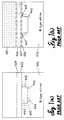
- patent 4291293 before the sealing of the glass and shows the poly-silicon layer 424 on top of the passivation 423 and with one diffused P-type crossing conductor 442 and with the insulating space-charge region 440 of the pn-junction 443 extending into the p-side to the line 444 and into the N-type substrate area 426 to line 445.
- the space-charge region 440 will extend with uniform thickness all around the p-conductor including the surface area.
- Fig. 1(b) shows the same structure after anodic bonding with the glass 415 bonded to the surface of the poly-silicon layer 424.
- Ionic contamination in the passivation over PN-junctions may not only lead to reduction in break-down voltages and cause leakages currents, but may also cause N-type inversion layers to be formed on lightly doped P-type areas between doped N-areas that should be insulated from each other.
- Such effects are well known for persons with knowledge in the field of semiconductor physics and are among others described in a semiconductor textbook by A.S. Grove: "Physics and Technology of Semiconductor Devices", Chapter 10, 11 and 12; John Wiley & Sons, Inc. (1967).
- the invention provides for different kinds of sensors requiring sealed cavities including electrical feed-throughs on each die to be built in a cost effective way as described and shown in detail in the following.
- the method is in particular suitable for making absolute pressure sensors with vacuum in the sealed cavity, accelerometers with controlled pressure in the area around a seismic mass-spring system and sealed cavities with controlled pressure for resonant structures and other types of functional devices.
- the method may also be used to build micropackages on the chip level around delicate structures that need to be protected against the environment such as different types of microactuators, hereby allowing low-cost plastic packaging to be used.
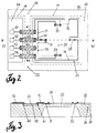
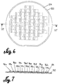
- FIG. 2 shows a cross-sectional view of one pressure sensor die 20 of a first silicon wafer 120 according to figs. 6, 7 and 8 including a pressure sensitive diaphragm 30 with four piezoresistors.
- Fig. 2 is a plan view of the same die 20.
- Said piezoresistors 31, 32, 33 and 34 are electrically connected to aluminium wire bonding pads for interconnection areas 51, 52, 53 and 54 via aluminium interconnection lines 71, 72, 73 and 74 and buried diffused conductors 41, 42, 43 and 44.
- These conductors are doped by ion implantation and buried under an N-type epitaxial layer 25 which also covers the N-type substrate 26.
- the method of making these buried conductors results in no steps on the surface of the first silicon wafer hereby taking advantage of the very smooth surfaces of polished silicon wafers in the sealing area of the structure to be made. This result in a reliable wafer lamination method with high yield and allowing high reliability sensors or functional devices to be made with low built-in stress as the sealing areas.
- the area on the surface of the die marked 22 is the area on which anodic bonding is to be performed, the line 17 indicating the periphery of the cavity of the glass and line 18 indicating the periphery of the via-hole of the glass needed for access to the aluminium wire-bonding and interconnection areas 51, 52, 53 and 54.
- the buried conductors are connected to the aluminium interconnection areas and lines via contact diffusions 60, 61 and contact holes in the passivation 28 as shown in the cross sectional view of fig. 3 where one buried diffused conductor 42 is contacted by P+ diffusions 60 and 61 at each end through the epitaxial layer 25.
- Figs. 4 and 5 show the silicon die 20 of figs.
- the glass member 14 of figs. 4 and 5 has a section 15 forming a recess in said glass member 14 and thus forming a sealed cavity 16 with a sealing interface area 23 bonding to the silicon member 20 after anodic bonding.
- fig. 5 it is possible to follow the electrical connection path from one of the outside wire bonding areas, e.g.
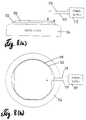
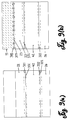
- the anodic bonding process itself is well known to persons working in the field of silicon microsensors and will not be described in any detail here. However, the principle will be briefly discussed with reference to figs. 8(a) and 8(b).
- the multichip silicon wafer 120 is placed together with the glass wafer 114 on a heated chuck 116 after the wafers are well aligned and placed in contact with each other.
- degC positive ions such as sodium ions in the glass will be mobile and will drift under the influence of an electric field by enforcing a voltage from a power supply 117 over the glass via the electrical connections and probes 118 and 119.
- the method according to the invention completely solves the problems related to the prior art of forming accumulation layers and/or inversion layers which affect the insulating PN-junction of the conductors.
- the use of buried conductors isolates the PN-junction of each of the buried conductors under the epitaxial layer and away from the influence of the ions from the glass.
- the ions from the glass will have an effect on the surface of the epitaxial layer only where no PN-junctions are located. This can be seen in fig. 9(a) and fig. 9(b) showing a small cross-sectional portion from the sealing area of the structure of fig. 3 and fig. 5, where fig. 9(a) shows a detailed structure before anodic bonding as seen from fig.
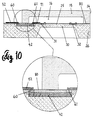
- the glass wafer 114 of fig. 7 can be replaced by a second silicon wafer with sputter deposited glass film on one of the surfaces.
- Fig. 11 shows a cross sectional view of this resulting structure with 140 being the second silicon member with the sputter deposited glass film 141 bonded to the first silicon member 20 forming a complete seal at area 122 over the crossing conductors 42.
- a vacuum reference volume 160 is in this case made by selective etching of a hole in a region 150 of the second silicon member 140.
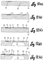
- the first multi-chip silicon wafer 120 of fig. 7 with pressure sensor die 20 as shown in fig. 3 can be processed by well known silicon process technology as explained in the following by referring to fig. 12(a)-(e). Processing starts as shown in fig. 12(a) with an N-type 1-0-0 single crystal substrate 26.
- the first photomask step defines the buried conductors 42 which are formed by ion implantation of boron using a photoresist as a mask layer and followed by a drive-in diffusion step. This will result in surface doping of insulated P-areas for the crossings without any steps in the surface at the location of the PN-junctions. This is followed by growing an epitaxial N-type layer 25 as shown in fig.
- the next two steps as shown in fig. 12(c) are to form the P-type contacts 60 and 61 at each end of the buried P-type conductor 42 by photomasking and doping and followed by patterning and doping the piezoresistive elements 31 and 32. Over the contacts 60, 61 and elements 31 and 32 is provided a passivation layer 28.
- the structure can now be completed by forming a diaphragm 30 by selective etching as shown in fig. 12(d) and by making contact holes through the passivation layer 28 and metal interconnection members 52 and 71 as shown in fig. 12(e).
- the structure is now ready to be anodically bonded to a glass member as shown in fig. 5 or a second silicon member with sputtered glass as shown in fig. 11.
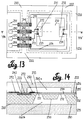
- the universal properties of the present invention can be shown by explaining a second example of an accelerometer built by using this method and as shown in fig. 13 and 14.
- a silicon accelerometer structure with seismic mass-spring system built into a first silicon member 220 is shown as part of fig. 14 and shown in plan view in fig. 13 as resulting from processing of a first wafer with a central seismic proof mass 230 hanging on two spring members 231 and 232 suspended from a frame section of silicon substrate 226.
- Piezoresistive elements 233 and 234 are electrically connected to outside bonding pads and aluminium interconnections members 251, 252, 253 and 254 via aluminium interconnection members 271, 272, 273 and 274 and buried diffused conductor crossings 241, 242, 243 and 244.
- Glass members 215 and 275 as seen in fig. 14 are anodically bonded to each side of the silicon member 220 at interface areas 222 and 280, thus forming a completely sealed cavity 260a and 260b around the seismic mass-spring system 230, 231, 232 of the accelerometer of said glass member 215.
- the distance between the proof-mass 230 and lid part 250 of said glass member 215 and/or the distance between the proof-mass 230 and the bottom glass member 275 can be used for mechanical overload protection of the travel of the proof-mass in mechanical shock situations and/or for squeezefilm damping by using a controlled atmosphere in the cavity.
- the figures 13 and 14 show a piezoresistive accelerometer with a half-bridge having resistors 233 and 234. It is obvious that resonant structures can be integrated and connected in the same way hereby making an accelerometer with resonant structure as detection principle.
- the present invention can be used for a large variety of functional devices which are to be sealed inside a cavity of controlled atmosphere or vacuum.
- functional devices could e.g. be connected in a manner known per se to contact areas inside the cavity, whether or not a diaphragm or spring-mass system is used.
Landscapes
- Engineering & Computer Science (AREA)
- Physics & Mathematics (AREA)
- General Physics & Mathematics (AREA)
- Microelectronics & Electronic Packaging (AREA)
- Manufacturing & Machinery (AREA)
- Chemical & Material Sciences (AREA)
- Analytical Chemistry (AREA)
- Pressure Sensors (AREA)
- Measuring Fluid Pressure (AREA)
- Packages (AREA)
- Measurement Of Force In General (AREA)
- Light Receiving Elements (AREA)
Applications Claiming Priority (2)
| Application Number | Priority Date | Filing Date | Title |
|---|---|---|---|
| US42166595A | 1995-04-12 | 1995-04-12 | |
| US421665 | 1995-04-12 |
Publications (3)
| Publication Number | Publication Date |
|---|---|
| EP0742581A2 true EP0742581A2 (fr) | 1996-11-13 |
| EP0742581A3 EP0742581A3 (fr) | 1997-05-02 |
| EP0742581B1 EP0742581B1 (fr) | 2002-11-27 |
Family
ID=23671517
Family Applications (1)
| Application Number | Title | Priority Date | Filing Date |
|---|---|---|---|
| EP96850075A Expired - Lifetime EP0742581B1 (fr) | 1995-04-12 | 1996-04-11 | Dispositif à cavité scellée |
Country Status (6)
| Country | Link |
|---|---|
| US (1) | US5591679A (fr) |
| EP (1) | EP0742581B1 (fr) |
| JP (1) | JP3073442B2 (fr) |
| KR (1) | KR100271386B1 (fr) |
| AT (1) | ATE228718T1 (fr) |
| DE (1) | DE69624973T2 (fr) |
Cited By (20)
| Publication number | Priority date | Publication date | Assignee | Title |
|---|---|---|---|---|
| WO1999016114A1 (fr) * | 1997-09-23 | 1999-04-01 | Infineon Technologies Ag | Procede de production d'une piece composite, et piece composite |
| WO1999035477A1 (fr) * | 1998-01-09 | 1999-07-15 | Robert Bosch Gmbh | Composant micromecanique |
| DE19857550A1 (de) * | 1998-12-14 | 2000-06-21 | Bosch Gmbh Robert | Verfahren zur Verkapselung von metallischen Mikrobauteilen |
| EP1096260A1 (fr) * | 1999-10-29 | 2001-05-02 | SensoNor asa | Capteur micromécanique |
| WO2001029890A3 (fr) * | 1999-10-19 | 2001-09-07 | Imego Ab | Procede concernant les liaisons anodiques |
| WO2001071303A3 (fr) * | 2000-03-23 | 2002-02-14 | Michael Burchard | Detecteur de pression et de temperature |
| DE10129821A1 (de) * | 2001-06-13 | 2003-01-02 | X Fab Ges Zur Fertigung Von Wa | Verfahren und Anordnung zum Passivieren anodischer Bondgebiete, die über elektrisch aktiven Strukturen von mikroelektromechanischen Systemen angeordnet sind (Microelectromechnical System: MEMS) |
| WO2003019201A1 (fr) * | 2001-08-24 | 2003-03-06 | Honeywell International Inc. | Systeme electromecanique micro-usine de silicium, a fermeture etanche, possedant des conducteurs diffuses |
| WO2004068094A3 (fr) * | 2003-01-31 | 2004-12-16 | Melexis Nv | Dispositif de mesure de l'acceleration et de la pression integre et son procede de fabrication |
| WO2005018798A1 (fr) | 2003-08-25 | 2005-03-03 | Casio Computer Co., Ltd. | Substrat a jonction et procede pour lier des substrats |
| EP1522521A1 (fr) | 2003-10-10 | 2005-04-13 | SensoNor asa | Capteur capacitif |
| FR2865575A1 (fr) * | 2004-01-23 | 2005-07-29 | Bosch Gmbh Robert | Procede pour emballer des pastilles semi-conductrices et structure de pastille semi-conductrice ainsi obtenue |
| EP0962275A3 (fr) * | 1998-06-03 | 2005-08-10 | Delphi Technologies, Inc. | Procédé de liaison de substrats micro-usinés utilisant une brasure |
| US6951797B1 (en) | 1999-10-19 | 2005-10-04 | Imego Ab | Method relating to anodic bonding |
| CN1307683C (zh) * | 2003-08-22 | 2007-03-28 | 沈阳仪表科学研究院 | 一种传感器小间隙非粘连静电封接方法 |
| DE10053307B4 (de) * | 2000-10-27 | 2008-06-26 | Eads Deutschland Gmbh | Kapsel für Mikrosensoren, Verfahren zur Verkapselung von Mikrosensoren und Kapselelement |
| EP1953516A1 (fr) | 2007-01-31 | 2008-08-06 | Infineon Technologies SensoNor AS | Capteur de pression micromécanique |
| DE102009019029A1 (de) * | 2008-06-19 | 2009-12-31 | Infineon Technologies Ag | Sensormodul |
| WO2015103220A1 (fr) | 2013-12-30 | 2015-07-09 | Robert Bosch Gmbh | Capteurs inertiels robustes |
| KR101985946B1 (ko) * | 2018-11-21 | 2019-06-04 | 호산엔지니어링(주) | Msg를 이용한 로드셀 장치 |
Families Citing this family (73)
| Publication number | Priority date | Publication date | Assignee | Title |
|---|---|---|---|---|
| US6316796B1 (en) | 1995-05-24 | 2001-11-13 | Lucas Novasensor | Single crystal silicon sensor with high aspect ratio and curvilinear structures |
| US6084257A (en) * | 1995-05-24 | 2000-07-04 | Lucas Novasensor | Single crystal silicon sensor with high aspect ratio and curvilinear structures |
| US6046840A (en) * | 1995-06-19 | 2000-04-04 | Reflectivity, Inc. | Double substrate reflective spatial light modulator with self-limiting micro-mechanical elements |
| US5866469A (en) * | 1996-06-13 | 1999-02-02 | Boeing North American, Inc. | Method of anodic wafer bonding |
| US6140144A (en) * | 1996-08-08 | 2000-10-31 | Integrated Sensing Systems, Inc. | Method for packaging microsensors |
| US5994161A (en) * | 1997-09-03 | 1999-11-30 | Motorola, Inc. | Temperature coefficient of offset adjusted semiconductor device and method thereof |
| DE19741428A1 (de) * | 1997-09-19 | 1999-04-01 | Siemens Ag | Halbleitersensor mit einem Grundkörper und wenigstens einem Verformungskörper |
| FR2770339B1 (fr) * | 1997-10-27 | 2003-06-13 | Commissariat Energie Atomique | Structure munie de contacts electriques formes a travers le substrat de cette structure et procede d'obtention d'une telle structure |
| US6074891A (en) * | 1998-06-16 | 2000-06-13 | Delphi Technologies, Inc. | Process for verifying a hermetic seal and semiconductor device therefor |
| US6278167B1 (en) | 1998-08-14 | 2001-08-21 | Infineon Technologies Ag | Semiconductor sensor with a base element and at least one deformation element |
| US6534340B1 (en) * | 1998-11-18 | 2003-03-18 | Analog Devices, Inc. | Cover cap for semiconductor wafer devices |
| US6232150B1 (en) * | 1998-12-03 | 2001-05-15 | The Regents Of The University Of Michigan | Process for making microstructures and microstructures made thereby |
| JP3567094B2 (ja) * | 1999-02-09 | 2004-09-15 | 株式会社日立製作所 | 回路内蔵型センサおよびそれを用いた圧力検出装置 |
| EP1110905A1 (fr) * | 1999-12-24 | 2001-06-27 | SensoNor asa | Dispositif micro-électromécanique |
| US6550337B1 (en) * | 2000-01-19 | 2003-04-22 | Measurement Specialties, Inc. | Isolation technique for pressure sensing structure |
| US6753638B2 (en) * | 2000-02-03 | 2004-06-22 | Calient Networks, Inc. | Electrostatic actuator for micromechanical systems |
| EP1307720A1 (fr) * | 2000-07-06 | 2003-05-07 | California Institute Of Technology | Capteur de pression a surface micro-usinee et application a haute pression |
| US6795605B1 (en) * | 2000-08-01 | 2004-09-21 | Cheetah Omni, Llc | Micromechanical optical switch |
| US6564642B1 (en) | 2000-11-02 | 2003-05-20 | Kavlico Corporation | Stable differential pressure measuring system |
| US6809424B2 (en) * | 2000-12-19 | 2004-10-26 | Harris Corporation | Method for making electronic devices including silicon and LTCC and devices produced thereby |
| EP1223420A3 (fr) | 2001-01-16 | 2003-07-09 | Fujikura Ltd. | Capteur de pression et son procédé de fabrication |
| US7145704B1 (en) * | 2003-11-25 | 2006-12-05 | Cheetah Omni, Llc | Optical logic gate based optical router |
| WO2002073673A1 (fr) * | 2001-03-13 | 2002-09-19 | Rochester Institute Of Technology | Commutateur micro-electromecanique et un procede de sa mise en oeuvre et de sa fabrication |
| US6581468B2 (en) | 2001-03-22 | 2003-06-24 | Kavlico Corporation | Independent-excitation cross-coupled differential-pressure transducer |
| WO2002097865A2 (fr) * | 2001-05-31 | 2002-12-05 | Rochester Institute Of Technology | Soupapes, agitateurs et pompes microfluidiques et procedes correspondants |
| US6841917B2 (en) * | 2001-06-11 | 2005-01-11 | Rochester Institute Of Technology | Electrostatic levitation and attraction systems and methods |
| KR100514240B1 (ko) | 2001-06-21 | 2005-09-13 | 미쓰비시덴키 가부시키가이샤 | 가속도 센서 및 그 제조방법 |
| US7378775B2 (en) * | 2001-10-26 | 2008-05-27 | Nth Tech Corporation | Motion based, electrostatic power source and methods thereof |
| US7211923B2 (en) * | 2001-10-26 | 2007-05-01 | Nth Tech Corporation | Rotational motion based, electrostatic power source and methods thereof |
| US7110671B1 (en) * | 2001-12-03 | 2006-09-19 | Cheetah Omni, Llc | Method and apparatus for scheduling communication using a star switching fabric |
| US6608370B1 (en) * | 2002-01-28 | 2003-08-19 | Motorola, Inc. | Semiconductor wafer having a thin die and tethers and methods of making the same |
| US7287328B2 (en) * | 2003-08-29 | 2007-10-30 | Rochester Institute Of Technology | Methods for distributed electrode injection |
| US7217582B2 (en) * | 2003-08-29 | 2007-05-15 | Rochester Institute Of Technology | Method for non-damaging charge injection and a system thereof |
| US6949807B2 (en) * | 2003-12-24 | 2005-09-27 | Honeywell International, Inc. | Signal routing in a hermetically sealed MEMS device |
| US20050172717A1 (en) * | 2004-02-06 | 2005-08-11 | General Electric Company | Micromechanical device with thinned cantilever structure and related methods |
| US8581308B2 (en) * | 2004-02-19 | 2013-11-12 | Rochester Institute Of Technology | High temperature embedded charge devices and methods thereof |
| US20050205951A1 (en) * | 2004-03-18 | 2005-09-22 | Honeywell Internatioanl, Inc. | Flip chip bonded micro-electromechanical system (MEMS) device |
| US20060037398A1 (en) * | 2004-08-19 | 2006-02-23 | Rich David B | Method for making an impact detector |
| NO321281B1 (no) * | 2004-09-15 | 2006-04-18 | Sintef | Infrarod kilde |
| FR2881224B1 (fr) * | 2005-01-21 | 2007-11-23 | Auxitrol Sa Sa | Ensemble de detection de la pression absolue d'un fluide |
| US20060202304A1 (en) * | 2005-03-11 | 2006-09-14 | Orr Raymond K | Integrated circuit with temperature-controlled component |
| US7470971B2 (en) * | 2005-05-13 | 2008-12-30 | Sarnoff Corporation | Anodically bonded ultra-high-vacuum cell |
| US7622782B2 (en) * | 2005-08-24 | 2009-11-24 | General Electric Company | Pressure sensors and methods of making the same |
| US20070074731A1 (en) * | 2005-10-05 | 2007-04-05 | Nth Tech Corporation | Bio-implantable energy harvester systems and methods thereof |
| JP5174673B2 (ja) * | 2005-10-14 | 2013-04-03 | エスティーマイクロエレクトロニクス エス.アール.エル. | 基板レベル・アセンブリを具えた電子装置及びその製造処理方法 |
| US7420817B2 (en) | 2006-01-09 | 2008-09-02 | Honeywell International Inc. | MEMS device seal using liquid crystal polymer |
| DE102007002725A1 (de) * | 2007-01-18 | 2008-07-31 | Fraunhofer-Gesellschaft zur Förderung der angewandten Forschung e.V. | Gehäuse für in mobilen Anwendungen eingesetzte mikromechanische und mikrooptische Bauelemente |
| JP5142742B2 (ja) * | 2007-02-16 | 2013-02-13 | 株式会社デンソー | 圧力センサおよびその製造方法 |
| US20080277747A1 (en) * | 2007-05-08 | 2008-11-13 | Nazir Ahmad | MEMS device support structure for sensor packaging |
| DE102007034888B3 (de) * | 2007-07-16 | 2009-01-22 | Fraunhofer-Gesellschaft zur Förderung der angewandten Forschung e.V. | Mikrosystem und Verfahren zum Herstellen eines Mikrosystems |
| US7644625B2 (en) * | 2007-12-14 | 2010-01-12 | Honeywell International Inc. | Differential pressure sense die based on silicon piezoresistive technology |
| US8643127B2 (en) * | 2008-08-21 | 2014-02-04 | S3C, Inc. | Sensor device packaging |
| EP2166330A1 (fr) * | 2008-09-22 | 2010-03-24 | GE Infrastructure Sensing, Inc. | Transducteur de pression miniature de type allongé et utilisable à une temperature élevée |
| US7775119B1 (en) | 2009-03-03 | 2010-08-17 | S3C, Inc. | Media-compatible electrically isolated pressure sensor for high temperature applications |
| EP2252077B1 (fr) | 2009-05-11 | 2012-07-11 | STMicroelectronics Srl | Ensemble de transducteur acoustique capacitif de type micro-électromécanique et paquet correspondant |
| IT1394898B1 (it) * | 2009-06-03 | 2012-07-20 | St Microelectronics Rousset | Giroscopio microelettromeccanico con attuazione a controllo di posizione e metodo per il controllo di un giroscopio microelettromeccanico |
| US7998777B1 (en) * | 2010-12-15 | 2011-08-16 | General Electric Company | Method for fabricating a sensor |
| FR3003246B1 (fr) | 2013-03-13 | 2017-12-22 | Commissariat Energie Atomique | Procede d'encapsulation de micro-dispositif par scellement anodique |
| JP5783297B2 (ja) * | 2013-08-06 | 2015-09-24 | 株式会社デンソー | 力学量センサ |
| US9470593B2 (en) | 2013-09-12 | 2016-10-18 | Honeywell International Inc. | Media isolated pressure sensor |
| US9102512B2 (en) | 2013-10-04 | 2015-08-11 | Analog Devices, Inc. | Sealed MEMS devices with multiple chamber pressures |
| US9764946B2 (en) | 2013-10-24 | 2017-09-19 | Analog Devices, Inc. | MEMs device with outgassing shield |
| DE102014202825B4 (de) | 2014-02-17 | 2023-06-07 | Robert Bosch Gmbh | Mikromechanisches Bauteil mit hermetischer Durchkontaktierung und Verfahren zur Herstellung eines mikromechanischen Bauteils mit einer hermetischen Durchkontaktierung |
| CN103792036B (zh) * | 2014-03-05 | 2016-01-20 | 中国电子科技集团公司第三十八研究所 | 气压与加速度传感器相集成的mems芯片及其制作方法 |
| US10032936B2 (en) | 2015-05-29 | 2018-07-24 | Seiko Epson Corporation | Method for manufacturing resistive element, method for manufacturing pressure sensor element, pressure sensor element, pressure sensor, altimeter, electronic apparatus, and moving object |
| JP2017053742A (ja) * | 2015-09-10 | 2017-03-16 | セイコーエプソン株式会社 | 電子デバイスの製造方法、電子デバイス、電子機器、および移動体 |
| US10446331B2 (en) | 2015-09-22 | 2019-10-15 | Analog Devices, Inc. | Wafer-capped rechargeable power source |
| US20170089792A1 (en) * | 2015-09-28 | 2017-03-30 | Merit Medical Systems, Inc. | Dampened pressure port |
| EP3211393A1 (fr) | 2016-02-29 | 2017-08-30 | ETH Zürich | Dispositif mems à l'aide d'une couche de dispositif en tant que membrane libérée |
| IT201700103489A1 (it) | 2017-09-15 | 2019-03-15 | St Microelectronics Srl | Metodo di fabbricazione di una membrana filtrante sottile, dispositivo trasduttore acustico includente la membrana filtrante, metodo di assemblaggio del dispositivo trasduttore acustico e sistema elettronico |
| US20210020455A1 (en) * | 2019-07-17 | 2021-01-21 | Nanya Technology Corporation | Conductive via structure |
| CN112174085B (zh) * | 2020-10-14 | 2024-09-06 | 广州市智芯禾科技有限责任公司 | 一种高温压力传感器芯片及其制备方法 |
| US12103843B2 (en) | 2021-01-20 | 2024-10-01 | Calient.Ai Inc. | MEMS mirror arrays with reduced crosstalk |
Family Cites Families (8)
| Publication number | Priority date | Publication date | Assignee | Title |
|---|---|---|---|---|
| US4023562A (en) * | 1975-09-02 | 1977-05-17 | Case Western Reserve University | Miniature pressure transducer for medical use and assembly method |
| JPS54131892A (en) * | 1978-04-05 | 1979-10-13 | Hitachi Ltd | Semiconductor pressure converter |
| JPS5544786A (en) * | 1978-09-27 | 1980-03-29 | Hitachi Ltd | Pressure sensor |
| JPH0712086B2 (ja) * | 1984-01-27 | 1995-02-08 | 株式会社日立製作所 | ダイヤフラムセンサの製造方法 |
| US4975390A (en) * | 1986-12-18 | 1990-12-04 | Nippondenso Co. Ltd. | Method of fabricating a semiconductor pressure sensor |
| JPH0810170B2 (ja) * | 1987-03-06 | 1996-01-31 | 株式会社日立製作所 | 半導体絶対圧力センサの製造方法 |
| JPH05273231A (ja) * | 1992-03-27 | 1993-10-22 | Toyoda Mach Works Ltd | 容量型加速度センサ |
| JP3257272B2 (ja) * | 1994-09-05 | 2002-02-18 | 株式会社デンソー | 力学量センサおよびその製造方法 |
-
1996
- 1996-01-30 US US08/593,848 patent/US5591679A/en not_active Expired - Lifetime
- 1996-04-11 JP JP08113021A patent/JP3073442B2/ja not_active Expired - Fee Related
- 1996-04-11 EP EP96850075A patent/EP0742581B1/fr not_active Expired - Lifetime
- 1996-04-11 DE DE69624973T patent/DE69624973T2/de not_active Expired - Lifetime
- 1996-04-11 AT AT96850075T patent/ATE228718T1/de not_active IP Right Cessation
- 1996-04-12 KR KR1019960010946A patent/KR100271386B1/ko not_active Expired - Fee Related
Cited By (30)
| Publication number | Priority date | Publication date | Assignee | Title |
|---|---|---|---|---|
| WO1999016114A1 (fr) * | 1997-09-23 | 1999-04-01 | Infineon Technologies Ag | Procede de production d'une piece composite, et piece composite |
| WO1999035477A1 (fr) * | 1998-01-09 | 1999-07-15 | Robert Bosch Gmbh | Composant micromecanique |
| DE19800574B4 (de) * | 1998-01-09 | 2013-11-14 | Robert Bosch Gmbh | Mikromechanisches Bauelement |
| US6465854B1 (en) | 1998-01-09 | 2002-10-15 | Robert Bosch Gmbh | Micromechanical component |
| EP0962275A3 (fr) * | 1998-06-03 | 2005-08-10 | Delphi Technologies, Inc. | Procédé de liaison de substrats micro-usinés utilisant une brasure |
| DE19857550A1 (de) * | 1998-12-14 | 2000-06-21 | Bosch Gmbh Robert | Verfahren zur Verkapselung von metallischen Mikrobauteilen |
| WO2001029890A3 (fr) * | 1999-10-19 | 2001-09-07 | Imego Ab | Procede concernant les liaisons anodiques |
| US6951797B1 (en) | 1999-10-19 | 2005-10-04 | Imego Ab | Method relating to anodic bonding |
| EP1096260A1 (fr) * | 1999-10-29 | 2001-05-02 | SensoNor asa | Capteur micromécanique |
| WO2001071303A3 (fr) * | 2000-03-23 | 2002-02-14 | Michael Burchard | Detecteur de pression et de temperature |
| DE10053307B4 (de) * | 2000-10-27 | 2008-06-26 | Eads Deutschland Gmbh | Kapsel für Mikrosensoren, Verfahren zur Verkapselung von Mikrosensoren und Kapselelement |
| DE10129821C2 (de) * | 2001-06-13 | 2003-06-18 | X Fab Semiconductor Foundries | Verfahren zum Passivieren anodischer Bondgebiete, die über elektrisch aktiven Strukturen von mikroelektromechanischen Systemen angeordnet sind (Microelectromechnical System: MEMS) |
| DE10129821A1 (de) * | 2001-06-13 | 2003-01-02 | X Fab Ges Zur Fertigung Von Wa | Verfahren und Anordnung zum Passivieren anodischer Bondgebiete, die über elektrisch aktiven Strukturen von mikroelektromechanischen Systemen angeordnet sind (Microelectromechnical System: MEMS) |
| US6906395B2 (en) | 2001-08-24 | 2005-06-14 | Honeywell International, Inc. | Hermetically sealed silicon micro-machined electromechanical system (MEMS) device having diffused conductors |
| WO2003019201A1 (fr) * | 2001-08-24 | 2003-03-06 | Honeywell International Inc. | Systeme electromecanique micro-usine de silicium, a fermeture etanche, possedant des conducteurs diffuses |
| WO2004068094A3 (fr) * | 2003-01-31 | 2004-12-16 | Melexis Nv | Dispositif de mesure de l'acceleration et de la pression integre et son procede de fabrication |
| CN1307683C (zh) * | 2003-08-22 | 2007-03-28 | 沈阳仪表科学研究院 | 一种传感器小间隙非粘连静电封接方法 |
| WO2005018798A1 (fr) | 2003-08-25 | 2005-03-03 | Casio Computer Co., Ltd. | Substrat a jonction et procede pour lier des substrats |
| US7205625B2 (en) | 2003-08-25 | 2007-04-17 | Casio Computer Co., Ltd. | Junction substrate and method of bonding substrates together |
| US7867346B2 (en) | 2003-08-25 | 2011-01-11 | Casio Computer Co., Ltd. | Junction substrate and method of bonding substrates together |
| EP1522521A1 (fr) | 2003-10-10 | 2005-04-13 | SensoNor asa | Capteur capacitif |
| FR2865575A1 (fr) * | 2004-01-23 | 2005-07-29 | Bosch Gmbh Robert | Procede pour emballer des pastilles semi-conductrices et structure de pastille semi-conductrice ainsi obtenue |
| EP1953516A1 (fr) | 2007-01-31 | 2008-08-06 | Infineon Technologies SensoNor AS | Capteur de pression micromécanique |
| DE102009019029A1 (de) * | 2008-06-19 | 2009-12-31 | Infineon Technologies Ag | Sensormodul |
| US8130506B2 (en) | 2008-06-19 | 2012-03-06 | Infineon Technologies Ag | Sensor module |
| DE102009019029B4 (de) * | 2008-06-19 | 2012-09-27 | Infineon Technologies Ag | Verfahren zur Herstellung eines Sensormoduls |
| US9177879B2 (en) | 2008-06-19 | 2015-11-03 | Infineon Technologies Ag | Sensor module |
| WO2015103220A1 (fr) | 2013-12-30 | 2015-07-09 | Robert Bosch Gmbh | Capteurs inertiels robustes |
| US10317211B2 (en) | 2013-12-30 | 2019-06-11 | Robert Bosch Gmbh | Robust inertial sensors |
| KR101985946B1 (ko) * | 2018-11-21 | 2019-06-04 | 호산엔지니어링(주) | Msg를 이용한 로드셀 장치 |
Also Published As
| Publication number | Publication date |
|---|---|
| DE69624973D1 (de) | 2003-01-09 |
| KR960037894A (ko) | 1996-11-19 |
| ATE228718T1 (de) | 2002-12-15 |
| DE69624973T2 (de) | 2003-08-28 |
| EP0742581A3 (fr) | 1997-05-02 |
| JPH08306936A (ja) | 1996-11-22 |
| JP3073442B2 (ja) | 2000-08-07 |
| EP0742581B1 (fr) | 2002-11-27 |
| KR100271386B1 (ko) | 2001-01-15 |
| US5591679A (en) | 1997-01-07 |
Similar Documents
| Publication | Publication Date | Title |
|---|---|---|
| US5591679A (en) | Sealed cavity arrangement method | |
| US5386142A (en) | Semiconductor structures having environmentally isolated elements and method for making the same | |
| US7247246B2 (en) | Vertical integration of a MEMS structure with electronics in a hermetically sealed cavity | |
| US7104129B2 (en) | Vertically integrated MEMS structure with electronics in a hermetically sealed cavity | |
| US6346742B1 (en) | Chip-scale packaged pressure sensor | |
| Li et al. | Low stress packaging of a micromachined accelerometer | |
| US6265246B1 (en) | Microcap wafer-level package | |
| US7026223B2 (en) | Hermetic electric component package | |
| US6146917A (en) | Fabrication method for encapsulated micromachined structures | |
| JP4388210B2 (ja) | ウエハパッケージの製造方法 | |
| TWI533438B (zh) | 半導體設備、半導體結構、以及半導體結構之形成方法 | |
| US5719069A (en) | One-chip integrated sensor process | |
| US6841861B2 (en) | MEMS package | |
| US6313529B1 (en) | Bump bonding and sealing a semiconductor device with solder | |
| US6828674B2 (en) | Hermetically sealed microstructure package | |
| US7259436B2 (en) | Micromechanical component and corresponding production method | |
| EP1167281A2 (fr) | Assemblage à l'échelle d'une puce pour montage en surface pour dispositifs electroniques et MEMS | |
| US20020017713A1 (en) | Microcap wafer-level package | |
| JP2003294451A (ja) | マイクロ慣性センサ及びその製造方法 | |
| US20070298542A1 (en) | Multiple internal seal ring micro-electro-mechanical system vacuum packaging method | |
| JPH05190872A (ja) | 半導体圧力センサおよびその製造方法 | |
| WO2016200346A1 (fr) | Procédé d'encapsulation hermétique pour dispositifs mems de type soi avec des traversées verticales intégrées | |
| US7023083B2 (en) | Multi-layer device and method for producing the same | |
| EP1199744A1 (fr) | Boítier de type micro-couvercle au niveau de plaquettes | |
| JP3173256B2 (ja) | 半導体加速度センサとその製造方法 |
Legal Events
| Date | Code | Title | Description |
|---|---|---|---|
| PUAI | Public reference made under article 153(3) epc to a published international application that has entered the european phase |
Free format text: ORIGINAL CODE: 0009012 |
|
| AK | Designated contracting states |
Kind code of ref document: A2 Designated state(s): AT BE CH DE DK ES FI FR GB GR IE IT LI LU MC NL PT SE |
|
| PUAL | Search report despatched |
Free format text: ORIGINAL CODE: 0009013 |
|
| AK | Designated contracting states |
Kind code of ref document: A3 Designated state(s): AT BE CH DE DK ES FI FR GB GR IE IT LI LU MC NL PT SE |
|
| 17P | Request for examination filed |
Effective date: 19970526 |
|
| 17Q | First examination report despatched |
Effective date: 19990824 |
|
| RAP1 | Party data changed (applicant data changed or rights of an application transferred) |
Owner name: SENSONOR ASA |
|
| GRAG | Despatch of communication of intention to grant |
Free format text: ORIGINAL CODE: EPIDOS AGRA |
|
| GRAG | Despatch of communication of intention to grant |
Free format text: ORIGINAL CODE: EPIDOS AGRA |
|
| GRAH | Despatch of communication of intention to grant a patent |
Free format text: ORIGINAL CODE: EPIDOS IGRA |
|
| GRAH | Despatch of communication of intention to grant a patent |
Free format text: ORIGINAL CODE: EPIDOS IGRA |
|
| GRAA | (expected) grant |
Free format text: ORIGINAL CODE: 0009210 |
|
| RAP1 | Party data changed (applicant data changed or rights of an application transferred) |
Owner name: SENSONOR ASA |
|
| AK | Designated contracting states |
Kind code of ref document: B1 Designated state(s): AT BE CH DE DK ES FI FR GB GR IE IT LI LU MC NL PT SE |
|
| PG25 | Lapsed in a contracting state [announced via postgrant information from national office to epo] |
Ref country code: NL Free format text: LAPSE BECAUSE OF FAILURE TO SUBMIT A TRANSLATION OF THE DESCRIPTION OR TO PAY THE FEE WITHIN THE PRESCRIBED TIME-LIMIT Effective date: 20021127 Ref country code: LI Free format text: LAPSE BECAUSE OF FAILURE TO SUBMIT A TRANSLATION OF THE DESCRIPTION OR TO PAY THE FEE WITHIN THE PRESCRIBED TIME-LIMIT Effective date: 20021127 Ref country code: IT Free format text: LAPSE BECAUSE OF FAILURE TO SUBMIT A TRANSLATION OF THE DESCRIPTION OR TO PAY THE FEE WITHIN THE PRE;WARNING: LAPSES OF ITALIAN PATENTS WITH EFFECTIVE DATE BEFORE 2007 MAY HAVE OCCURRED AT ANY TIME BEFORE 2007. THE CORRECT EFFECTIVE DATE MAY BE DIFFERENT FROM THE ONE RECORDED.SCRIBED TIME-LIMIT Effective date: 20021127 Ref country code: GR Free format text: LAPSE BECAUSE OF FAILURE TO SUBMIT A TRANSLATION OF THE DESCRIPTION OR TO PAY THE FEE WITHIN THE PRESCRIBED TIME-LIMIT Effective date: 20021127 Ref country code: FI Free format text: LAPSE BECAUSE OF FAILURE TO SUBMIT A TRANSLATION OF THE DESCRIPTION OR TO PAY THE FEE WITHIN THE PRESCRIBED TIME-LIMIT Effective date: 20021127 Ref country code: CH Free format text: LAPSE BECAUSE OF FAILURE TO SUBMIT A TRANSLATION OF THE DESCRIPTION OR TO PAY THE FEE WITHIN THE PRESCRIBED TIME-LIMIT Effective date: 20021127 Ref country code: BE Free format text: LAPSE BECAUSE OF FAILURE TO SUBMIT A TRANSLATION OF THE DESCRIPTION OR TO PAY THE FEE WITHIN THE PRESCRIBED TIME-LIMIT Effective date: 20021127 Ref country code: AT Free format text: LAPSE BECAUSE OF FAILURE TO SUBMIT A TRANSLATION OF THE DESCRIPTION OR TO PAY THE FEE WITHIN THE PRESCRIBED TIME-LIMIT Effective date: 20021127 |
|
| REF | Corresponds to: |
Ref document number: 228718 Country of ref document: AT Date of ref document: 20021215 Kind code of ref document: T |
|
| REG | Reference to a national code |
Ref country code: GB Ref legal event code: FG4D |
|
| REG | Reference to a national code |
Ref country code: CH Ref legal event code: EP |
|
| REG | Reference to a national code |
Ref country code: IE Ref legal event code: FG4D |
|
| REF | Corresponds to: |
Ref document number: 69624973 Country of ref document: DE Date of ref document: 20030109 |
|
| PG25 | Lapsed in a contracting state [announced via postgrant information from national office to epo] |
Ref country code: SE Free format text: LAPSE BECAUSE OF FAILURE TO SUBMIT A TRANSLATION OF THE DESCRIPTION OR TO PAY THE FEE WITHIN THE PRESCRIBED TIME-LIMIT Effective date: 20030227 Ref country code: PT Free format text: LAPSE BECAUSE OF FAILURE TO SUBMIT A TRANSLATION OF THE DESCRIPTION OR TO PAY THE FEE WITHIN THE PRESCRIBED TIME-LIMIT Effective date: 20030227 Ref country code: DK Free format text: LAPSE BECAUSE OF FAILURE TO SUBMIT A TRANSLATION OF THE DESCRIPTION OR TO PAY THE FEE WITHIN THE PRESCRIBED TIME-LIMIT Effective date: 20030227 |
|
| PGFP | Annual fee paid to national office [announced via postgrant information from national office to epo] |
Ref country code: GB Payment date: 20030320 Year of fee payment: 8 |
|
| PGFP | Annual fee paid to national office [announced via postgrant information from national office to epo] |
Ref country code: FR Payment date: 20030328 Year of fee payment: 8 |
|
| PG25 | Lapsed in a contracting state [announced via postgrant information from national office to epo] |
Ref country code: LU Free format text: LAPSE BECAUSE OF NON-PAYMENT OF DUE FEES Effective date: 20030411 Ref country code: IE Free format text: LAPSE BECAUSE OF NON-PAYMENT OF DUE FEES Effective date: 20030411 |
|
| PG25 | Lapsed in a contracting state [announced via postgrant information from national office to epo] |
Ref country code: MC Free format text: LAPSE BECAUSE OF NON-PAYMENT OF DUE FEES Effective date: 20030430 |
|
| NLV1 | Nl: lapsed or annulled due to failure to fulfill the requirements of art. 29p and 29m of the patents act | ||
| PG25 | Lapsed in a contracting state [announced via postgrant information from national office to epo] |
Ref country code: ES Free format text: LAPSE BECAUSE OF FAILURE TO SUBMIT A TRANSLATION OF THE DESCRIPTION OR TO PAY THE FEE WITHIN THE PRESCRIBED TIME-LIMIT Effective date: 20030529 |
|
| REG | Reference to a national code |
Ref country code: CH Ref legal event code: PL |
|
| ET | Fr: translation filed | ||
| PLBE | No opposition filed within time limit |
Free format text: ORIGINAL CODE: 0009261 |
|
| STAA | Information on the status of an ep patent application or granted ep patent |
Free format text: STATUS: NO OPPOSITION FILED WITHIN TIME LIMIT |
|
| 26N | No opposition filed |
Effective date: 20030828 |
|
| REG | Reference to a national code |
Ref country code: IE Ref legal event code: MM4A |
|
| PG25 | Lapsed in a contracting state [announced via postgrant information from national office to epo] |
Ref country code: GB Free format text: LAPSE BECAUSE OF NON-PAYMENT OF DUE FEES Effective date: 20040411 |
|
| GBPC | Gb: european patent ceased through non-payment of renewal fee |
Effective date: 20040411 |
|
| PG25 | Lapsed in a contracting state [announced via postgrant information from national office to epo] |
Ref country code: FR Free format text: LAPSE BECAUSE OF NON-PAYMENT OF DUE FEES Effective date: 20041231 |
|
| REG | Reference to a national code |
Ref country code: FR Ref legal event code: ST |
|
| REG | Reference to a national code |
Ref country code: DE Ref legal event code: R081 Ref document number: 69624973 Country of ref document: DE Owner name: INFINEON TECHNOLOGIES AG, DE Free format text: FORMER OWNER: SENSONOR ASA, HORTEN, NO Effective date: 20111012 |
|
| PGFP | Annual fee paid to national office [announced via postgrant information from national office to epo] |
Ref country code: DE Payment date: 20120619 Year of fee payment: 17 |
|
| PG25 | Lapsed in a contracting state [announced via postgrant information from national office to epo] |
Ref country code: DE Free format text: LAPSE BECAUSE OF NON-PAYMENT OF DUE FEES Effective date: 20131101 |
|
| REG | Reference to a national code |
Ref country code: DE Ref legal event code: R119 Ref document number: 69624973 Country of ref document: DE Effective date: 20131101 |