EP0768593A2 - Circuit générateur de courant de référence - Google Patents
Circuit générateur de courant de référence Download PDFInfo
- Publication number
- EP0768593A2 EP0768593A2 EP96116361A EP96116361A EP0768593A2 EP 0768593 A2 EP0768593 A2 EP 0768593A2 EP 96116361 A EP96116361 A EP 96116361A EP 96116361 A EP96116361 A EP 96116361A EP 0768593 A2 EP0768593 A2 EP 0768593A2
- Authority
- EP
- European Patent Office
- Prior art keywords
- circuit
- voltage
- reference current
- resistor ladder
- mos transistor
- Prior art date
- Legal status (The legal status is an assumption and is not a legal conclusion. Google has not performed a legal analysis and makes no representation as to the accuracy of the status listed.)
- Withdrawn
Links
- 238000009966 trimming Methods 0.000 claims description 4
- 230000008859 change Effects 0.000 abstract description 7
- 238000004519 manufacturing process Methods 0.000 abstract description 5
- 108010086600 N(2),N(2)-dimethylguanosine-26-methyltransferase Proteins 0.000 description 8
- 102100034541 tRNA (guanine(26)-N(2))-dimethyltransferase Human genes 0.000 description 8
- 238000010586 diagram Methods 0.000 description 7
- 239000004065 semiconductor Substances 0.000 description 7
- 101100343585 Arabidopsis thaliana LNG1 gene Proteins 0.000 description 6
- 101150110861 TRM2 gene Proteins 0.000 description 6
- 238000013459 approach Methods 0.000 description 2
- 230000005669 field effect Effects 0.000 description 2
- 230000004048 modification Effects 0.000 description 2
- 238000012986 modification Methods 0.000 description 2
- 229920006395 saturated elastomer Polymers 0.000 description 2
- 230000009471 action Effects 0.000 description 1
- 230000007547 defect Effects 0.000 description 1
- 238000000034 method Methods 0.000 description 1
- 229910021420 polycrystalline silicon Inorganic materials 0.000 description 1
- 229920005591 polysilicon Polymers 0.000 description 1
- 230000008569 process Effects 0.000 description 1
Images


Classifications
-
- G—PHYSICS
- G11—INFORMATION STORAGE
- G11C—STATIC STORES
- G11C7/00—Arrangements for writing information into, or reading information out from, a digital store
-
- G—PHYSICS
- G05—CONTROLLING; REGULATING
- G05F—SYSTEMS FOR REGULATING ELECTRIC OR MAGNETIC VARIABLES
- G05F3/00—Non-retroactive systems for regulating electric variables by using an uncontrolled element, or an uncontrolled combination of elements, such element or such combination having self-regulating properties
- G05F3/02—Regulating voltage or current
- G05F3/08—Regulating voltage or current wherein the variable is DC
- G05F3/10—Regulating voltage or current wherein the variable is DC using uncontrolled devices with non-linear characteristics
- G05F3/16—Regulating voltage or current wherein the variable is DC using uncontrolled devices with non-linear characteristics being semiconductor devices
- G05F3/20—Regulating voltage or current wherein the variable is DC using uncontrolled devices with non-linear characteristics being semiconductor devices using diode- transistor combinations
- G05F3/26—Current mirrors
- G05F3/262—Current mirrors using field-effect transistors only
-
- G—PHYSICS
- G05—CONTROLLING; REGULATING
- G05F—SYSTEMS FOR REGULATING ELECTRIC OR MAGNETIC VARIABLES
- G05F3/00—Non-retroactive systems for regulating electric variables by using an uncontrolled element, or an uncontrolled combination of elements, such element or such combination having self-regulating properties
- G05F3/02—Regulating voltage or current
- G05F3/08—Regulating voltage or current wherein the variable is DC
- G05F3/10—Regulating voltage or current wherein the variable is DC using uncontrolled devices with non-linear characteristics
- G05F3/16—Regulating voltage or current wherein the variable is DC using uncontrolled devices with non-linear characteristics being semiconductor devices
- G05F3/20—Regulating voltage or current wherein the variable is DC using uncontrolled devices with non-linear characteristics being semiconductor devices using diode- transistor combinations
- G05F3/24—Regulating voltage or current wherein the variable is DC using uncontrolled devices with non-linear characteristics being semiconductor devices using diode- transistor combinations wherein the transistors are of the field-effect type only
- G05F3/242—Regulating voltage or current wherein the variable is DC using uncontrolled devices with non-linear characteristics being semiconductor devices using diode- transistor combinations wherein the transistors are of the field-effect type only with compensation for device parameters, e.g. channel width modulation, threshold voltage, processing, or external variations, e.g. temperature, loading, supply voltage
Definitions
- the present invention relates to a reference current generating circuit, and more specifically to a reference current generating circuit suitable to be incorporated in a MOS semiconductor integrated circuit.
- JP-A-59-066725 proposed a reference current generating circuit (constant current circuit) as shown in Figure 1.
- the shown prior art constant current circuit includes a differential amplifier 11 having a non-inverting input (+) connected to receive an input reference voltage V 0 , an NMOS transistor (N-channel metal-oxide-semiconductor field effect transistor) 12 having a gate connected to an output of the differential amplifier 11 and a source connected to an inverting input (-) of the differential amplifier 11, and a constant current generating reference resistor 13 having a resistance R 0 having one end connected at a connected node "a" between the source of the transistor 12 and the inverting input of the differential amplifier 11. The other end of the resistor 13 is grounded.
- a drain of the transistor 12 is connected to a constant current output OUT2.
- the integrated circuit is required to have output terminals for the external resistor, the number of output terminals of the integrated circuit is increased as a matter of course.
- the constant current generating reference resistor 13 is internally formed in the integrated circuit in the form of a diffused resistor, in place of the external resistor, it is not possible to realize a high precise reference current generating circuit because the variation of the resistance of the diffused resistor dependently upon a temperature change is large if an internal resistor was simply formed in the inside of the integrate circuit.
- Another object of the present invention is to provide a reference current generating circuit suitable to be incorporated in a MOS semiconductor integrated circuit and capable of generating a high precise reference current without being influenced by variation of the threshold V T of the transistor and a temperature change.
- a reference current generating circuit comprising a reference voltage generating means, a resistor ladder circuit connected to the reference voltage generating means and having a predetermined number of taps for outputting a corresponding number of different divided voltages obtained from a voltage generated by the reference voltage generating means, a control circuit connected to the predetermined number of taps of the resistor ladder circuit, for outputting a selected divided voltage of the different divided voltages, and a MOS transistor having a gate connected to receive the selected divided voltage and a source connected to a reference power supply terminal, a current flowing through a drain of the MOS transistor being extracted as an output reference current.
- the gate voltage of the MOS transistor is controlled by the control circuit to a level which enables the MOS transistor to generate a desired constant current, by selecting one of a plurality of different divided voltages obtained by the resistor ladder circuit from the reference voltage generated by the reference voltage generating means. Accordingly, a reference current generating circuit can be realized, which is capable of supplying a reference current having a high precision and a high stability in relation to a variation of the threshold V T of the MOS transistor caused by a variation in the manufacturing process and a temperature change. On the other hand, an external resistor, which was required in the prior art reference current generating circuit, becomes unnecessary. Therefore, the reference current generating circuit in accordance with the present invention is suitable to be incorporated in an integrated circuit, and can reduce the cost of the semiconductor device.
- FIG. 2 there is shown a circuit diagram of a first embodiment of the reference current generating circuit in accordance with the present invention.
- the shown first embodiment includes a reference voltage generating circuit for generating a reference voltage V REF , and a resistor ladder circuit (resistor string) 2 composed of a number of series-connected resistors R and having one end connected to an output terminal of the reference voltage generating circuit 1 and the other end connected to a low voltage power supply terminal V SS .
- This resistor ladder circuit 2 includes a predetermined number of taps for outputting a corresponding number of different divided voltages obtained from the reference voltage V REF .
- the shown embodiment also includes a control circuit 3 connected to the predetermined number of taps of the resistor ladder circuit 2, for outputting a selected divided voltage of the different divided voltages, and an NMOS transistor 4 having a gate connected to an output of the control circuit 3.
- the control circuit 3 includes switches SW 1 to SW X of the same number as that of the taps of the resistor ladder circuit 2. One end of each of the switches SW 1 to SW X is connected to a corresponding one tap of the taps of the resistor ladder circuit 2, and the other end of the switches SW 1 to SW X are connected in common to the output of the control circuit 3, which is connected to the gate of the NMOS transistors 4.
- a source of the NMOS transistor 4 is connected to low voltage power supply terminal V SS , and a drain of the NMOS transistor 4 is connected to an output terminal OUT.
- the resistor ladder circuit is formed of "n" unitary resistors having the same resistance R, namely, the resistor ladder circuit 2 is equally divided by “n".
- “n” is not smaller than 4, but in the shown embodiment, "n" is larger than 10.
- a potential on different connection nodes between the taps of the resistor ladder circuit 2 and the switches SW 1 to SW X of the control circuit 3 can be expressed as ((n-3)/n) ⁇ V REF , ((n-4)/n) ⁇ V REF , ((n-5)/n) ⁇ V REF , • • •.
- I REF K (V G - V SS -V T ) 2
- the closed switch is changed to another closed switch in the control circuit 3 so as to change the output gate voltage V G , thereby to realize the output current I REF corresponding to the desired predetermined value.
- FIG. 3 there is shown a detailed circuit diagram of a second embodiment of the reference current generating circuit in accordance with the present invention.
- the reference voltage generating circuit 1 includes a differential amplifier 9 having an offset voltage V OS and an equal-divided resistor ladder circuit 2, which are connected to constitute a non-inverting amplifier generating a reference voltage at its output.
- a non-inverting input of the differential amplifier 9 is connected to the offset voltage V OS , and the output of the differential amplifier 9 is connected at a node "A" to one end of the resistor ladder circuit 2, the other end of which is connected to a low voltage power supply terminal V SS
- An inverting input of the differential amplifier 9 is connected to a suitable intermediate point of the resistor ladder circuit 2, so that a stable reference voltage is outputted from the output of the differential amplifier 9.
- a ladder resistor circuit for dividing the reference voltage generated by the reference voltage generating circuit 1 is not independently provided, but is used in common to the voltage trimming resistor ladder circuit 2 internally provided in the reference voltage generating circuit 1.
- different divided voltages of the reference voltage V A generated in the resistor ladder circuit 2 are used not only for a voltage trimming for making the the reference voltage V A at a constant value, but also supplied to the control circuit 3.
- the resistor ladder circuit 2 is equally divided by "5", and voltage of four nodes B, C, D and E are supplied to the control circuit 3.
- the control circuit 3 of the second embodiment includes a pair of control signal input terminals TRM1 and TRM2, a pair of inverters 7 and 8, six transfer gates (pass transistors) 10A, 10B, 10C, 10D, 10E and 10F each formed of an NMOS transistor, which are connected as shown.
- the node B is connected to a source of the transfer gate transistor 10C having a gate connected to the control signal input terminal TRM1
- the node C is connected to a source of the transfer gate transistor 10E having a gate connected to an output of the inverter 7 having an input connected to the control signal input terminal TRM1.
- the node D is connected to a source of the transfer gate transistor 10D having a gate connected to the control signal input terminal TRM1, and the node E is connected to a source of the transfer gate transistor 10F having a gate connected to the output of the inverter 7.
- a drain of each of the transfer gate transistors 10C and 10E is connected in common to a source of the transfer gate transistor 10A having a gate connected to an output of the inverter 8 having an input connected to the control signal input terminal TRM2.
- a drain of each of the transfer gate transistors 10D and 10F is connected in common to a source of the transfer gate transistor 10B having a gate connected to the control signal input terminal TRM2.
- a drain of each of the transfer gate transistors 10A and 10B is connected in common to a node "G" to constitute an output of the control circuit 3.
- the six transfer gate transistors 10A, 10B, 10C, 10D, 10E and 10F constitute a so-called tree structure between the gate of NMOS transistor 4 and the nodes "B", “C”, “D” and “E” of the resistor ladder circuit 2.
- a source of the NMOS transistor 4 is connected to the low voltage power supply terminal V SS , and a drain of the NMOS transistor 4 is connected to a drain of a PMOS (P-channel metal-oxide-semiconductor field effect transistor) 5.
- the drain of the PMOS transistor 5 is connected to a gate of the PMOS transistor 5 itself and also connected to a gate of another PMOS transistor 6.
- a source of these PMOS transistors 5 and 6 are connected to a high voltage power supply terminal V DD .
- a drain of the PMOS transistor 6 constitutes a current output and is connected to an output terminal OUT1.
- a drain current I REF of the NMOS transistor 4 is determined by the output voltage V G of the control circuit 3, and this drain current I REF is supplied to the current mirror circuit composed of the PMOS transistors 5 and 6 and connected between the high voltage power supply terminal V DD and the NMOS transistor 4, so that an output current I REF1 corresponding to the drain current I REF is outputted from the output terminal OUT1.
- the PMOS transistors 5 and 6 are of the same size as mentioned above, but, it would be a matter of course to persons skilled in the art that, by adjusting the size ratio of the PMOS transistors 5 and 6 of the current mirror circuit, it is possible to make the output current I REF1 outputted from the output terminal OUT1, to desired times the drain current I REF of the NMOS transistor 4 (which constitutes an input current path or a reference current path of the current minor circuit).
- the resistor dividing ratio of the voltage trimming resistor ladder circuit 2 is adjusted.
- the voltage V A is adjusted to the desired value by adjusting or changing the intermediate point of the resistor ladder circuit 2 connected to the inverting input of the differential amplifier 9.
- the control signal of a low level is supplied to the control signal input terminals TRM1 and TRM2. In this condition, therefore, the transfer gate transistors 10E, 10F and 10A are turned on, and the transfer gate transistors 10C, 10D and 10B are turned off. Accordingly, the node “C” is connected to the node "G", so that the voltage (3/5)V A of the node “C” is outputted to the node "G".
- I REF K (V G - V SS - V T ) 2
- a drain current I REFA K (V G - V SS - V TA ) 2 (I REFA ⁇ I REF )
- the gate voltage of the NMOS transistor 4 is adjusted. Namely, the gate voltage of the NMOS transistor 4 is adjusted to V GA (V GA > V G ).
- the control signal supplied to the control signal input terminal TRM1 is brought to a high level, and on the other hand, the control signal supplied to the control signal input terminal TRM2 is maintained at the low level.
- the transfer gate transistors 10C, 10D and 10A are turned on, and the transfer gate transistors 10E, 10F and 10B are turned off.
- the node "B" is connected to the node "G", so that the voltage (4/5)V A of the node "B" is outputted to the node "G".
- the voltage on the node "G” becomes V GA (V GA > V G ), with the result that the current I REFA approaches or becomes equal to I REF .
- a drain current I REFB K (V G - V SS - V TB ) 2 (I REFB > I REF )
- the gate voltage of the NMOS transistor 4 is adjusted to V GB (V GB ⁇ V G ).
- both of the control signals supplied to the control signal input terminals TRM1 and TRM are brought to a high level.
- the transfer gate transistors 10C, 10D and 10B are turned on, and the transfer gate transistors 10E, 10F and 10A are turned off.
- the node "D" is connected to the node "G", so that the voltage (2/5)V A of the node "D” is outputted to the node "G".
- the voltage on the node "G” becomes V GB (V GB ⁇ V G ), with the result that the current I REFB approaches or becomes equal to I REF .
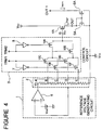
- FIG 4 there is shown a detailed circuit diagram of a third embodiment of the reference current generating circuit in accordance with the present invention, which is a modification of the second embodiment. Therefore, in Figure 4, elements similar to those shown in Figure 3 are given the same Reference Numerals.
- the third embodiment includes a PMOS transistor 4A in place of the NMOS transistor 4 in the second embodiment, and a pair of NMOS transistors 5A and 6A in place of the PMOS transistors 5 and 6 of the current mirror circuit in the second embodiment.
- a gate of the PMOS transistor 4A is connected to the node ''G, and a source of the PMOS transistor 4A is connected to the high voltage power supply terminal V DD .
- a drain of the PMOS transistor 4A is connected to a drain and a gate of the NMOS transistor 5A and a gate of the NMOS transistor 6A, which have a source connected in common to the low voltage power supply terminal V SS .
- a drain of the NMOS transistor 6A is connected to the output terminal OUT1 and constitutes a reference current output. Therefore, this third embodiment supplies a sink type reference current I REF1 .
- the second embodiment supplies a source type reference current I REF1 . This is only one difference between the second and third embodiments, and therefore, further explanation of the third embodiment will be omitted.
- the number of taps of the resistor ladder circuit 2 for supplying different divided voltages to the gate of the MOS transistor 4 or 4A was four, but in order to generate a more precise reference current I REF , the number of taps of the resistor ladder circuit 2 can be increased, for example, to 8, 16, 32, etc, by finely dividing the ladder resistor. If the number of taps is increased, the number of transfer gates in the control circuit 3 is correspondingly increased, and the bit number of the control signal is increased to 3, 4, 5, etc.
- the above mentioned second and third embodiments has four taps in the resistor ladder circuit only for simplification of description, and therefore, the present invention is in no way limited to these embodiments. Namely, it should be noted that the present invention is in no way limited to the details of the illustrated structures but changes and modifications may be made within the scope of the appended claims. Therefore, for example, the resistors of the resistor ladder circuit can be formed of polysilicon resistor in place of the diffused resistor.
- the reference current generating circuit in accordance with the present invention is characterized in that the gate voltage of the MOS transistor for generating the reference current, is controlled by a selected one of a plurality of different divided voltages obtained by an internally provided resistor ladder circuit from a reference voltage. Accordingly, it is possible to supply the reference current having a high precision and a high stability in relation to a variation of the threshold V T of the MOS transistor caused by a variation in the manufacturing process and a temperature change. On the other hand, an external resistor, which was required in the prior art reference current generating circuit, becomes unnecessary, and the whole of the reference current generating circuit can be realized in an integrated circuit. Therefore, the reference current generating circuit in accordance with the present invention is suitable to be incorporated in an integrated circuit, and can reduce the cost of the semiconductor device.
Landscapes
- Engineering & Computer Science (AREA)
- Microelectronics & Electronic Packaging (AREA)
- Physics & Mathematics (AREA)
- Nonlinear Science (AREA)
- Electromagnetism (AREA)
- General Physics & Mathematics (AREA)
- Radar, Positioning & Navigation (AREA)
- Automation & Control Theory (AREA)
- Control Of Electrical Variables (AREA)
- Continuous-Control Power Sources That Use Transistors (AREA)
- Control Of Voltage And Current In General (AREA)
- Amplifiers (AREA)
Applications Claiming Priority (2)
| Application Number | Priority Date | Filing Date | Title |
|---|---|---|---|
| JP289318/95 | 1995-10-11 | ||
| JP7289318A JP2917877B2 (ja) | 1995-10-11 | 1995-10-11 | 基準電流発生回路 |
Publications (2)
| Publication Number | Publication Date |
|---|---|
| EP0768593A2 true EP0768593A2 (fr) | 1997-04-16 |
| EP0768593A3 EP0768593A3 (fr) | 1998-01-21 |
Family
ID=17741645
Family Applications (1)
| Application Number | Title | Priority Date | Filing Date |
|---|---|---|---|
| EP96116361A Withdrawn EP0768593A3 (fr) | 1995-10-11 | 1996-10-11 | Circuit générateur de courant de référence |
Country Status (5)
| Country | Link |
|---|---|
| US (1) | US6377113B1 (fr) |
| EP (1) | EP0768593A3 (fr) |
| JP (1) | JP2917877B2 (fr) |
| KR (1) | KR100225825B1 (fr) |
| TW (1) | TW371372B (fr) |
Cited By (1)
| Publication number | Priority date | Publication date | Assignee | Title |
|---|---|---|---|---|
| CN107742498A (zh) * | 2017-11-24 | 2018-02-27 | 京东方科技集团股份有限公司 | 参考电压电路、参考电压提供模组和显示装置 |
Families Citing this family (20)
| Publication number | Priority date | Publication date | Assignee | Title |
|---|---|---|---|---|
| JP2002354195A (ja) * | 2001-05-29 | 2002-12-06 | Hamamatsu Photonics Kk | 信号処理回路および固体撮像装置 |
| JP3903770B2 (ja) * | 2001-11-08 | 2007-04-11 | 日本電気株式会社 | データ線駆動回路 |
| KR100543318B1 (ko) * | 2002-10-07 | 2006-01-20 | 주식회사 하이닉스반도체 | 부스팅 전압 제어회로 |
| US6891357B2 (en) * | 2003-04-17 | 2005-05-10 | International Business Machines Corporation | Reference current generation system and method |
| US7061304B2 (en) * | 2004-01-28 | 2006-06-13 | International Business Machines Corporation | Fuse latch with compensated programmable resistive trip point |
| JP4385811B2 (ja) * | 2004-03-24 | 2009-12-16 | 株式会社デンソー | 定電流回路 |
| US8106862B2 (en) * | 2004-05-19 | 2012-01-31 | Sharp Kabushiki Kaisha | Liquid crystal display device for reducing influence of voltage drop in time-division driving, method for driving the same, liquid crystal television having the same and liquid crystal monitor having the same |
| US7296247B1 (en) * | 2004-08-17 | 2007-11-13 | Xilinx, Inc. | Method and apparatus to improve pass transistor performance |
| KR100775057B1 (ko) | 2004-12-13 | 2007-11-08 | 삼성전자주식회사 | 트랜지스터 정합 특성이 향상된 데이터 드라이브 집적회로를 구비한 디스플레이 장치 |
| JP4848689B2 (ja) * | 2005-07-11 | 2011-12-28 | セイコーエプソン株式会社 | 半導体集積回路 |
| JP2007226627A (ja) * | 2006-02-24 | 2007-09-06 | Seiko Instruments Inc | ボルテージレギュレータ |
| JP5088031B2 (ja) * | 2007-08-01 | 2012-12-05 | 富士電機株式会社 | 定電流・定電圧回路 |
| JP5318676B2 (ja) * | 2009-06-25 | 2013-10-16 | ルネサスエレクトロニクス株式会社 | 半導体装置 |
| JP2011015259A (ja) * | 2009-07-03 | 2011-01-20 | Renesas Electronics Corp | 半導体集積回路装置およびその試験方法 |
| JP2011053957A (ja) * | 2009-09-02 | 2011-03-17 | Toshiba Corp | 参照電流生成回路 |
| KR101389620B1 (ko) * | 2011-10-28 | 2014-04-29 | 에스케이하이닉스 주식회사 | 멀티 레귤레이터 회로 및 이를 구비한 집적회로 |
| JP6232925B2 (ja) * | 2013-10-28 | 2017-11-22 | 富士電機株式会社 | 入力回路 |
| US9252713B2 (en) | 2014-02-27 | 2016-02-02 | Qualcomm Incorporated | Bias circuits and methods for stacked devices |
| JP2024077674A (ja) * | 2022-11-29 | 2024-06-10 | エイブリック株式会社 | 基準電流源 |
| US12566464B2 (en) * | 2023-08-21 | 2026-03-03 | Himax Imaging Limited | Power ground noise reduction system capable of reducing noise voltage interference |
Family Cites Families (15)
| Publication number | Priority date | Publication date | Assignee | Title |
|---|---|---|---|---|
| JPS5463662A (en) * | 1977-10-28 | 1979-05-22 | Nec Corp | Current supply circuit |
| US4198622A (en) * | 1978-02-21 | 1980-04-15 | National Semiconductor Corporation | Double digital-to-analog converter |
| US4354175A (en) * | 1980-05-01 | 1982-10-12 | Mostek Corporation | Analog/digital converter utilizing a single column of analog switches |
| US4331913A (en) * | 1980-10-02 | 1982-05-25 | Bell Telephone Laboratories, Incorporated | Precision negative impedance circuit with calibration |
| JPS5966725A (ja) * | 1982-10-07 | 1984-04-16 | Nippon Denso Co Ltd | 定電流回路 |
| JPS6331224A (ja) | 1986-07-24 | 1988-02-09 | Fuji Electric Co Ltd | A/d変換サンプル値の精度改善方式 |
| JPH02145012A (ja) * | 1988-11-26 | 1990-06-04 | Nec Corp | 基準電圧トリミング回路 |
| JPH03172906A (ja) * | 1989-12-01 | 1991-07-26 | Hitachi Ltd | トリミング回路 |
| JP3365804B2 (ja) * | 1993-01-12 | 2003-01-14 | 株式会社日立製作所 | 通信回線駆動回路、及びインタフェース用lsi、並びに通信端末装置 |
| JPH06243678A (ja) * | 1993-02-19 | 1994-09-02 | Hitachi Ltd | ダイナミック型ramとそのプレート電圧設定方法及び情報処理システム |
| JP3156447B2 (ja) * | 1993-06-17 | 2001-04-16 | 富士通株式会社 | 半導体集積回路 |
| JPH07170188A (ja) | 1993-12-14 | 1995-07-04 | Yamaha Corp | Daコンバータ回路 |
| US5640122A (en) * | 1994-12-16 | 1997-06-17 | Sgs-Thomson Microelectronics, Inc. | Circuit for providing a bias voltage compensated for p-channel transistor variations |
| US5568084A (en) * | 1994-12-16 | 1996-10-22 | Sgs-Thomson Microelectronics, Inc. | Circuit for providing a compensated bias voltage |
| US5504447A (en) * | 1995-06-07 | 1996-04-02 | United Memories Inc. | Transistor programmable divider circuit |
-
1995
- 1995-10-11 JP JP7289318A patent/JP2917877B2/ja not_active Expired - Lifetime
-
1996
- 1996-10-11 EP EP96116361A patent/EP0768593A3/fr not_active Withdrawn
- 1996-10-11 KR KR1019960045182A patent/KR100225825B1/ko not_active Expired - Fee Related
- 1996-10-11 TW TW085112409A patent/TW371372B/zh active
- 1996-10-11 US US08/729,399 patent/US6377113B1/en not_active Expired - Fee Related
Cited By (2)
| Publication number | Priority date | Publication date | Assignee | Title |
|---|---|---|---|---|
| CN107742498A (zh) * | 2017-11-24 | 2018-02-27 | 京东方科技集团股份有限公司 | 参考电压电路、参考电压提供模组和显示装置 |
| CN107742498B (zh) * | 2017-11-24 | 2021-02-09 | 京东方科技集团股份有限公司 | 参考电压电路、参考电压提供模组和显示装置 |
Also Published As
| Publication number | Publication date |
|---|---|
| US6377113B1 (en) | 2002-04-23 |
| KR100225825B1 (ko) | 1999-10-15 |
| KR970023370A (ko) | 1997-05-30 |
| JP2917877B2 (ja) | 1999-07-12 |
| TW371372B (en) | 1999-10-01 |
| EP0768593A3 (fr) | 1998-01-21 |
| JPH09106316A (ja) | 1997-04-22 |
Similar Documents
| Publication | Publication Date | Title |
|---|---|---|
| EP0768593A2 (fr) | Circuit générateur de courant de référence | |
| JP3315652B2 (ja) | 電流出力回路 | |
| US4636742A (en) | Constant-current source circuit and differential amplifier using the same | |
| EP0585755B1 (fr) | Circuit pour générer une tension de référence MOS compensée en température pour des applications à tension basse et des grandes plages de fonctionnement | |
| US6225855B1 (en) | Reference voltage generation circuit using source followers | |
| KR0148732B1 (ko) | 반도체 소자의 기준전압 발생회로 | |
| US7880512B2 (en) | Output driver circuit | |
| US7592862B2 (en) | Digital temperature sensing device using temperature depending characteristic of contact resistance | |
| KR950010048B1 (ko) | 기판 전위 검출 회로를 가진 반도체 집적 회로 장치 | |
| EP0573240A2 (fr) | Générateur de tension de référence | |
| US5434534A (en) | CMOS voltage reference circuit | |
| US6040735A (en) | Reference voltage generators including first and second transistors of same conductivity type | |
| US5057722A (en) | Delay circuit having stable delay time | |
| US6133764A (en) | Comparator circuit and method | |
| KR101080560B1 (ko) | 트랜스컨덕턴스 조정 회로 | |
| US5814981A (en) | Voltage circuit for generating multiple stable voltages | |
| US6275100B1 (en) | Reference voltage generators including first and second transistors of same conductivity type and at least one switch | |
| US20020027808A1 (en) | Differential output circuit | |
| US5570038A (en) | Semiconductor integrated circuit device with data output circuit | |
| KR100370679B1 (ko) | 레벨시프트회로 | |
| US5936436A (en) | Substrate potential detecting circuit | |
| KR0172436B1 (ko) | 반도체 장치의 기준전압 발생회로 | |
| US5870045A (en) | D/A converter | |
| JP4355710B2 (ja) | Mos型基準電圧発生回路 | |
| JPH09186294A (ja) | 電圧発生回路及び半導体装置 |
Legal Events
| Date | Code | Title | Description |
|---|---|---|---|
| PUAI | Public reference made under article 153(3) epc to a published international application that has entered the european phase |
Free format text: ORIGINAL CODE: 0009012 |
|
| AK | Designated contracting states |
Kind code of ref document: A2 Designated state(s): DE FR GB |
|
| PUAL | Search report despatched |
Free format text: ORIGINAL CODE: 0009013 |
|
| AK | Designated contracting states |
Kind code of ref document: A3 Designated state(s): DE FR GB |
|
| 17P | Request for examination filed |
Effective date: 19971211 |
|
| 17Q | First examination report despatched |
Effective date: 19991228 |
|
| STAA | Information on the status of an ep patent application or granted ep patent |
Free format text: STATUS: THE APPLICATION HAS BEEN WITHDRAWN |
|
| 18W | Application withdrawn |
Withdrawal date: 20000621 |