EP0777329A2 - Un circuit logique BIMOS commandable directement par un bloc de circuit CMOS constitué sur le même chip - Google Patents
Un circuit logique BIMOS commandable directement par un bloc de circuit CMOS constitué sur le même chip Download PDFInfo
- Publication number
- EP0777329A2 EP0777329A2 EP96119177A EP96119177A EP0777329A2 EP 0777329 A2 EP0777329 A2 EP 0777329A2 EP 96119177 A EP96119177 A EP 96119177A EP 96119177 A EP96119177 A EP 96119177A EP 0777329 A2 EP0777329 A2 EP 0777329A2
- Authority
- EP
- European Patent Office
- Prior art keywords
- logic
- bipolar
- transistors
- single chip
- pair
- Prior art date
- Legal status (The legal status is an assumption and is not a legal conclusion. Google has not performed a legal analysis and makes no representation as to the accuracy of the status listed.)
- Withdrawn
Links
Images


Classifications
-
- H—ELECTRICITY
- H03—ELECTRONIC CIRCUITRY
- H03K—PULSE TECHNIQUE
- H03K19/00—Logic circuits, i.e. having at least two inputs acting on one output; Inverting circuits
-
- H—ELECTRICITY
- H03—ELECTRONIC CIRCUITRY
- H03K—PULSE TECHNIQUE
- H03K3/00—Circuits for generating electric pulses; Monostable, bistable or multistable circuits
- H03K3/02—Generators characterised by the type of circuit or by the means used for producing pulses
- H03K3/021—Generators characterised by the type of circuit or by the means used for producing pulses by the use, as active elements, of more than one type of element or means, e.g. BIMOS, composite devices such as IGBT
-
- H—ELECTRICITY
- H03—ELECTRONIC CIRCUITRY
- H03K—PULSE TECHNIQUE
- H03K19/00—Logic circuits, i.e. having at least two inputs acting on one output; Inverting circuits
- H03K19/0175—Coupling arrangements; Interface arrangements
- H03K19/017509—Interface arrangements
- H03K19/017518—Interface arrangements using a combination of bipolar and field effect transistors [BIFET]
- H03K19/017527—Interface arrangements using a combination of bipolar and field effect transistors [BIFET] with at least one differential stage
-
- H—ELECTRICITY
- H03—ELECTRONIC CIRCUITRY
- H03K—PULSE TECHNIQUE
- H03K3/00—Circuits for generating electric pulses; Monostable, bistable or multistable circuits
- H03K3/02—Generators characterised by the type of circuit or by the means used for producing pulses
- H03K3/26—Generators characterised by the type of circuit or by the means used for producing pulses by the use, as active elements, of bipolar transistors with internal or external positive feedback
- H03K3/28—Generators characterised by the type of circuit or by the means used for producing pulses by the use, as active elements, of bipolar transistors with internal or external positive feedback using means other than a transformer for feedback
- H03K3/281—Generators characterised by the type of circuit or by the means used for producing pulses by the use, as active elements, of bipolar transistors with internal or external positive feedback using means other than a transformer for feedback using at least two transistors so coupled that the input of one is derived from the output of another, e.g. multivibrator
- H03K3/286—Generators characterised by the type of circuit or by the means used for producing pulses by the use, as active elements, of bipolar transistors with internal or external positive feedback using means other than a transformer for feedback using at least two transistors so coupled that the input of one is derived from the output of another, e.g. multivibrator bistable
- H03K3/288—Generators characterised by the type of circuit or by the means used for producing pulses by the use, as active elements, of bipolar transistors with internal or external positive feedback using means other than a transformer for feedback using at least two transistors so coupled that the input of one is derived from the output of another, e.g. multivibrator bistable using additional transistors in the input circuit
- H03K3/2885—Generators characterised by the type of circuit or by the means used for producing pulses by the use, as active elements, of bipolar transistors with internal or external positive feedback using means other than a transformer for feedback using at least two transistors so coupled that the input of one is derived from the output of another, e.g. multivibrator bistable using additional transistors in the input circuit the input circuit having a differential configuration
Definitions
- the present invention relates generally to improved techniques in an IC (integrated circuit) chip, and more specifically to a digital circuit which includes bipolar and unipolar transistors and which is arranged in a manner wherein it can be directly controlled by a CMOS (complementary metal-oxide semiconductor) logic formed on the same chip as the digital circuit.
- CMOS complementary metal-oxide semiconductor
- this digital circuit will be referred to as a BiMOS (bipolar MOS) logic.
- a conventional IC block for interfacing between the network and the user's terminal (e.g., PC) and processing data.
- An optical fiber is not shown in Fig. 1 because it is irrelevant to the present invention.
- a single IC chip 10 is generally comprised of an ECL (emitter-coupled logic) block 12 and a CMOS IC block 14.
- the ECL block 12 which interfaces the network with the user terminal, is provided with a demultiplexer (DEMUX) 16 and a multiplexer (MUX) 18.
- the single IC chip 10 further includes an ECL-level I/O (input/output) buffer 20, a level translator 22, and a CMOS-level I/O buffer 24.
- a serial data received by the user terminal and transmitted therefrom is as high as 622Mbps (mega bits per second) by way of example.
- the ECL block 12 uses bipolar transistors in a nonsaturating mode and thus the block 12 is able to attain very high speed data processing.
- the transistors in the ECL block 12 do not switch full-on or full-off, but swing above and below a given bias voltage.
- the ECL block 12 has the inherent disadvantages of high power consumption and low logic swing (600mV for example), it is a common practice to use an ECL logic where very high speed is essential.
- CMOS logics exhibit a data processing speed lower than the ECL circuit, it is typical to use the CMOS logics because the CMOS logics require the least power among the existing digital ICs and can be operated over a wide range of power-supply voltages (3V-5V for example).
- the logic swing of the ECL circuit is very small (about 600mV (for example)) compared with that of the CMOS circuit which is exemplified as 3V-5V (viz., supply voltages).
- the ECL block 12 must be interfaced with the CMOS block 14 using the level-translator 22.
- reducing the number of level-translators has been proposed in a paper entitled "0.5 micron Low-power BiMOS Gate Array for B-ISDN 622 Mb/s User-Network Interface" by Yasushi Hayakawa, et al., 1994 IEEE, pages 607-610.
- this paper fails to present any suggestion that the ECL block can be directly controlled by the CMOS block without the use of the level-translator.
- an aspect of the present invention resides in a single chip integrated circuit (IC) which includes: a bipolar logic, a complementary metal-oxide semiconductor (CMOS) logic, and a level translator which interfaces the bipolar logic with the CMOS logic.
- the single chip IC comprises: a MOS transistor logic means, combined with the bipolar logic, for receiving a control signal which controls an operation of the bipolar logic, the control signal being directly applied to the MOS transistor logic means from the CMOS.
- the present invention resides in an arrangement of an IC chip which generally includes, in combination, an improved BiMOS block and a CMOS block. More specifically, the BiMOS block can be directly controlled by the CMOS block. That is, according to the present invention, there is no need to convert the logic level of BiMOS control signals issued from the CMOS block. Therefore, the level-translator can be rendered simpler in configuration and/or operation.
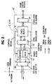
- Fig. 2 is a block diagram schematically showing the above mentioned IC chip (depicted by 10') to which the present invention is applicable.
- the blocks of Fig. 2, which are essentially identical with the counterparts of Fig. 1, are identified by the same numerals.
- each of the blocks of Fig. 2, which corresponds to that of Fig. 1, is represented by the same numeral plus a prime.
- Fig. 3A is a diagram showing a latch which includes a plurality of bipolar transistors for temporarily holding incoming data, and which can be set or reset using MOS transistors.
- the circuit of Fig. 3A is a BiMOS circuit in that it includes both bipolar and unipolar (MOS) transistors.
- the circuit of Fig. 3A is presented in preparation for describing a set/reset type mater-slave D flip-flop shown in Fig. 4A which is directly relevant to the present invention.
- the latch shown in Fig. 3A is provided between a power source VCC and a ground terminal GND and, includes resistors R1-R3, bipolar transistors Q1-Q6, n-channel MOS transistors Q7 and Q8, and a constant current-source (depicted by Ics).
- Ics constant current-source
- the transistors Q1 and Q2 form a differential pair (differential amplifier) at a data input side, and are respectively supplied with differential data D and /D at the bases thereof (the notation "/" means a bar over the following letter(s) in the accompanying drawings).
- the emitters of the transistors Q1 and Q2 are directly coupled and further coupled to the collector of the transistor Q3.
- the transistors Q4 and Q5 form another differential pair at a data latch side.
- the emitters of the transistors Q4 and Q5 are directly coupled and further coupled to the collector of the transistor Q6.
- the emitters of the transistors Q3 and Q6 are directly coupled and further coupled to a ground terminal GND via the current source Ics.
- the transistors Q3 and Q6 receive respectively differential clocks /CLK and CLK at the bases thereof, and constitute a differential pair.
- Voltages appearing at junctions 30 and 32 are outputs /OUT and OUT which change their logic levels in a differential manner.
- a current flow path from VCC to GND is changed depending on the ON and OFF states of the transistors Q1-Q6 and therefore, the bipolar portion of Fig. 3A is referred to as a current switch (or current mode switch (CML)).
- a current switch or current mode switch (CML)
- the two differential pairs exhibit a first differential stage of the current switch, while the transistors Q3 and Q6 form a second differential stage of the current switch.
- the n-channel MOS transistors Q7 and Q8 have their sources directly coupled and further coupled to the current source Ics.
- Set/reset signals S and R are respectively applied to the gates of the transistors Q7 and Q8 to fix the outputs OUT and /OUT.
- the clocks CLK and /CLK respectively assume low and high levels respectively and, simultaneously, the data D assumes a high level (namely, the data /D assumes a low level). Therefore, the transistors Q3 and Q6 are rendered conductive and non-conductive, respectively. Since the transistor Q2 is in a non-conductive state in the instant case, a current path is established from VCC to GND through the resistors R1 and R2, the transistors Q1 and Q3, and the current source Ics. This means that the outputs OUT and /OUT exhibit respectively high and low levels.
- the second row of the truth table shows that the clocks CLK and /CLX, as in the above case, respectively assume low and high levels.
- the data D assumes a low level while the data /D takes on a high level. Therefore, since the transistor Q1 is rendered non-conductive, a current flows from VCC to GND by way of the resistors R1 and R3, the transistors Q2 and Q3, and the current source Ics. Accordingly, the outputs OUT and /OUT respectively assume low and high levels in this case.
- the n-channel MOS transistors Q7 and Q8 are respectively rendered conductive and non-conductive.
- the outputs OUT and /OUT are set to high and low levels respectively (the fourth row of the truth table).
- the transistors Q7 and Q8 are rendered non-conductive and conductive, respectively.
- the outputs OUT and /OUT are reset to low and high levels respectively (the fifth row of the truth table).
- the set and reset signals S and R both assume high levels, the outputs OUT and /OUT become uncertain.
- Fig. 4A is a circuit diagram showing a set/reset type master-slave D flip-flop which is comprised of a combination of two latches of the nature shown in Fig. 3A. That is, two set/reset type latches (designated by A and B) are arranged in tandem as shown in Fig. 4A.
- the elements of latch A, which correspond to those of Fig. 3A, are depicted by the same notations, while the corresponding elements of latch B, are represented by the same notations plus primes.
- a truth table depicting the operation of the circuit of Fig. 4A is shown in Fig. 4B.
- master-slave D flip-flop The operation of master-slave D flip-flop is well known in the art and therefore, only a brief description thereof will be given.
- the clock CLK goes high, the incoming data D and /D are acquired whereby the outputs OUT and /OUT assume the same values as the acquired incoming data D and /D (the third and fourth rows of the truth table of Fig. 4B).
- the outputs OUT and /OUT are held.
- the clock CLK again goes high, the next incoming data D and /D are held in the flip-flop of Fig. 4A. This means that the output of data D and /D is delayed by one clock cycle.
- the D flip-flop of Fig. 4A is set and reset in a manner which has been described with reference to Figs. 3A and 3B. That is, the set/reset signals S and R are applied to the gates of the MOS transistors Q7, Q8, Q7' and Q8'. This implies that the signals S and R can be directly derived from the CMOS block 14 (Fig. 2).
- the 1:4 DEMUX 48 includes a plurality of conventional high speed bipolar flip-flops FF1-FF8 and a master-slave D flip-flop 50 which corresponds to the circuit of Fig. 4A. More specifically, the flip-flops FF9 and FF10 are essentially identical to the circuits A and B of Fig. 4A, respectively. It is to be noted that the set signal S shown in Fig. 4A is not used in this case. However, it goes without saying that the set signal S can be used instead of the reset signal R. It is quite easy for those skilled in the art to expand the 1:4 DEMUX to a 1:8 DEMUX (for example).
- a pair of differential input data Din and /Din are applied, as a serial data, to the DEMUX 48 from the ECL-level I/O buffer 20 (Fig. 2). Further, a reset signal R is directly applied to the D flip-flop 50 from the CMOS block 14 (Fig. 2).
- the master-slave D flip-flop 50 When the reset signal R is applied to the flip-flops FF9 and FF10, the master-slave D flip-flop 50 generates, from the flip-flop FF10, a clock 52 whose period is four (4) times the original clock CLK (and /CLK).
- the flip-flops FF1 to FF4 successively latch the respective incoming data 1, 2, 3, ... each time the clock CLK goes high, and apply respectively the outputs thereof to the flip-flops FF8-FF5 in a manner illustrated.
- the flip-flops FF5-FF8 generate four parallel data which are applied to the level translator 22 (Fig. 2).
- the flip-flops FF1-FF4 successively acquire the incoming data Din and /Din.
- the flip-flops FF5-FF8 remain disable because the clock 52 is not applied thereto.
- the present invention renders it possible for the CMOS block to directly apply the control signal (set and/or reset signal) to the BiMOS logic which operates at a very high speed using bipolar transistors.
- the control signal no longer requires level translation before being applied from the CMOS block to the high speed bipolar circuit of the BiMOS logic.
Landscapes
- Engineering & Computer Science (AREA)
- Computer Hardware Design (AREA)
- Physics & Mathematics (AREA)
- Computing Systems (AREA)
- General Engineering & Computer Science (AREA)
- Mathematical Physics (AREA)
- Power Engineering (AREA)
- Logic Circuits (AREA)
- Metal-Oxide And Bipolar Metal-Oxide Semiconductor Integrated Circuits (AREA)
- Semiconductor Integrated Circuits (AREA)
Applications Claiming Priority (2)
| Application Number | Priority Date | Filing Date | Title |
|---|---|---|---|
| JP7338188A JPH09153593A (ja) | 1995-11-30 | 1995-11-30 | BiMOS論理回路 |
| JP338188/95 | 1995-11-30 |
Publications (2)
| Publication Number | Publication Date |
|---|---|
| EP0777329A2 true EP0777329A2 (fr) | 1997-06-04 |
| EP0777329A3 EP0777329A3 (fr) | 1997-06-11 |
Family
ID=18315759
Family Applications (1)
| Application Number | Title | Priority Date | Filing Date |
|---|---|---|---|
| EP96119177A Withdrawn EP0777329A3 (fr) | 1995-11-30 | 1996-11-29 | Un circuit logique BIMOS commandable directement par un bloc de circuit CMOS constitué sur le même chip |
Country Status (4)
| Country | Link |
|---|---|
| US (1) | US5850155A (fr) |
| EP (1) | EP0777329A3 (fr) |
| JP (1) | JPH09153593A (fr) |
| KR (1) | KR970031338A (fr) |
Cited By (1)
| Publication number | Priority date | Publication date | Assignee | Title |
|---|---|---|---|---|
| EP1463201A1 (fr) * | 2003-03-25 | 2004-09-29 | Infineon Technologies AG | Diviseur de fréquence commandé par injection d'un signal de courant |
Families Citing this family (15)
| Publication number | Priority date | Publication date | Assignee | Title |
|---|---|---|---|---|
| US5978379A (en) | 1997-01-23 | 1999-11-02 | Gadzoox Networks, Inc. | Fiber channel learning bridge, learning half bridge, and protocol |
| US7430171B2 (en) | 1998-11-19 | 2008-09-30 | Broadcom Corporation | Fibre channel arbitrated loop bufferless switch circuitry to increase bandwidth without significant increase in cost |
| DE10035414A1 (de) * | 2000-07-20 | 2002-02-07 | Infineon Technologies Ag | Integrierter Schaltkreis mit Referenzstromversorgung |
| US6861888B2 (en) * | 2002-01-16 | 2005-03-01 | Agilent Technologies, Inc. | High-sensitivity differential data latch system |
| US8656178B2 (en) * | 2002-04-18 | 2014-02-18 | International Business Machines Corporation | Method, system and program product for modifying content usage conditions during content distribution |
| JP4246965B2 (ja) * | 2002-05-31 | 2009-04-02 | 株式会社日立製作所 | 半導体集積回路装置 |
| US6798263B1 (en) * | 2002-11-25 | 2004-09-28 | Applied Micro Circuits Corporation | Reset feature for a low voltage differential latch |
| US7129750B2 (en) * | 2003-07-30 | 2006-10-31 | Stmicroelectronics Pvt. Ltd. | CMOS to PECL voltage level converter |
| US7215170B1 (en) * | 2003-09-16 | 2007-05-08 | Cypress Semiconductor Corp. | Low voltage logic circuit with set and/or reset functionality |
| JP4247181B2 (ja) * | 2004-11-30 | 2009-04-02 | 富士通株式会社 | サンプルホールド回路 |
| US7474127B2 (en) * | 2006-01-06 | 2009-01-06 | Intel Corporation | Signal converter |
| US7808274B2 (en) * | 2007-12-28 | 2010-10-05 | Semiconductor Components Industries, Llc | Monolithically integrated multiplexer-translator-demultiplexer circuit and method |
| US8612469B2 (en) * | 2008-02-21 | 2013-12-17 | Globalenglish Corporation | Network-accessible collaborative annotation tool |
| KR101105814B1 (ko) * | 2010-06-04 | 2012-01-17 | 한국과학기술원 | 주파수 분주기 |
| RU2699684C2 (ru) * | 2016-01-12 | 2019-09-09 | Дмитрий Александрович Баландин | Низковольтный d-триггер с асинхронной установкой значения на основе эмиттерно-связанной логики |
Family Cites Families (16)
| Publication number | Priority date | Publication date | Assignee | Title |
|---|---|---|---|---|
| JPS61273012A (ja) * | 1985-05-28 | 1986-12-03 | Nec Ic Microcomput Syst Ltd | フリツプフロツプ回路 |
| JPH0775315B2 (ja) * | 1985-07-19 | 1995-08-09 | 株式会社日立製作所 | バッファ回路 |
| US4791628A (en) * | 1987-10-16 | 1988-12-13 | American Telephone And Telegraph Company, At&T Bell Labs | High-speed demultiplexer circuit |
| JPH0290627A (ja) * | 1988-09-28 | 1990-03-30 | Nec Corp | 入力回路 |
| JPH02130016A (ja) * | 1988-11-09 | 1990-05-18 | Fujitsu Ltd | Eclラッチ回路 |
| JPH02192213A (ja) * | 1989-01-20 | 1990-07-30 | Hitachi Ltd | 半導体集積回路装置 |
| JPH0379121A (ja) * | 1989-08-23 | 1991-04-04 | Hitachi Ltd | 半導体集積回路装置 |
| US5047980A (en) * | 1990-08-17 | 1991-09-10 | Unisys Corporation | BiCMOS memory having memory cells connected directly to address decoders |
| EP0476341B1 (fr) * | 1990-08-29 | 1997-01-15 | Motorola, Inc. | Circuit logique BICMOS avec une sortie CML |
| US5311082A (en) * | 1991-12-17 | 1994-05-10 | National Semiconductor Corporation | CMOS to ECL level translator |
| JP3138048B2 (ja) * | 1992-02-27 | 2001-02-26 | 三洋電機株式会社 | ラッチ回路 |
| US5287016A (en) * | 1992-04-01 | 1994-02-15 | International Business Machines Corporation | High-speed bipolar-field effect transistor (BI-FET) circuit |
| US5298810A (en) * | 1992-09-11 | 1994-03-29 | Cypress Semiconductor Corporation | BiCMOS CMOS/ECL data multiplexer |
| DE4231178C2 (de) * | 1992-09-17 | 1994-07-21 | Siemens Ag | Speicherelement |
| JPH06162782A (ja) * | 1992-11-17 | 1994-06-10 | Hitachi Ltd | 半導体集積回路装置 |
| JP3538442B2 (ja) * | 1993-09-20 | 2004-06-14 | 富士通株式会社 | レベル変換回路 |
-
1995
- 1995-11-30 JP JP7338188A patent/JPH09153593A/ja active Pending
-
1996
- 1996-11-29 KR KR1019960059985A patent/KR970031338A/ko not_active Ceased
- 1996-11-29 EP EP96119177A patent/EP0777329A3/fr not_active Withdrawn
- 1996-12-02 US US08/758,664 patent/US5850155A/en not_active Expired - Fee Related
Non-Patent Citations (1)
| Title |
|---|
| None |
Cited By (1)
| Publication number | Priority date | Publication date | Assignee | Title |
|---|---|---|---|---|
| EP1463201A1 (fr) * | 2003-03-25 | 2004-09-29 | Infineon Technologies AG | Diviseur de fréquence commandé par injection d'un signal de courant |
Also Published As
| Publication number | Publication date |
|---|---|
| US5850155A (en) | 1998-12-15 |
| KR970031338A (ko) | 1997-06-26 |
| JPH09153593A (ja) | 1997-06-10 |
| EP0777329A3 (fr) | 1997-06-11 |
Similar Documents
| Publication | Publication Date | Title |
|---|---|---|
| US5850155A (en) | BIMOS logic circuit directly controllable by a CMOS block formed on same IC chip | |
| US6867716B2 (en) | Synchronous data serialization circuit | |
| US7724057B2 (en) | Current-controlled CMOS logic family | |
| US6992505B1 (en) | Structures and methods of implementing a pass gate multiplexer with pseudo-differential input signals | |
| EP0232969B1 (fr) | Circuit de conversion de niveau | |
| US5214317A (en) | CMOS to ECL translator with incorporated latch | |
| US5900745A (en) | Semiconductor device including input buffer circuit capable of amplifying input signal with low amplitude in high speed and under low current consumption | |
| US6320422B1 (en) | Complementary source coupled logic | |
| US4733111A (en) | Sequential-logic basic element in CMOS technology operating by a single clock signal | |
| US5412380A (en) | Electronic crosspoint switching device operating at a high signal transmission rate | |
| CA2089429C (fr) | Tampon d'entree ttl-cmos eliminateur de bruit a faible consommation d'energie | |
| JPH0212691A (ja) | 集積回路 | |
| USRE35483E (en) | Switching matrix crosspoint | |
| US4258273A (en) | Universal register | |
| WO2003075138A1 (fr) | Horloge a faible gigue destinee a un emetteur-recepteur multi-gigabit dans une porte programmable par l'utilisateur | |
| US3947829A (en) | Logical circuit apparatus | |
| EP1376867A1 (fr) | Convertisseur différentiel rapide de logique CMOS en ECL | |
| US6781420B2 (en) | Symmetric differential logic circuits | |
| US4900954A (en) | Mixed CML/ECL macro circuitry | |
| EP0209829B1 (fr) | Elément de base de logique séquentielle et réseau électrique en technologie CMOS | |
| Kurisu et al. | 2.8 Gb/s 176 mW byte-interleaved and 3.0 Gb/s 118 mW bit-interleaved 8: 1 multiplexers | |
| US6760277B1 (en) | Arrangement for generating multiple clocks in field programmable gate arrays of a network test system | |
| JP3980776B2 (ja) | 入力バッファ回路および双方向バッファ並びに半導体集積回路 | |
| JP2004186710A (ja) | フリップフロップ回路およびクロック信号によってデータを保持し同期させる方法 | |
| KR100348123B1 (ko) | 래치 회로 |
Legal Events
| Date | Code | Title | Description |
|---|---|---|---|
| PUAI | Public reference made under article 153(3) epc to a published international application that has entered the european phase |
Free format text: ORIGINAL CODE: 0009012 |
|
| PUAL | Search report despatched |
Free format text: ORIGINAL CODE: 0009013 |
|
| AK | Designated contracting states |
Kind code of ref document: A2 Designated state(s): DE IT |
|
| AK | Designated contracting states |
Kind code of ref document: A3 Designated state(s): DE IT |
|
| 17P | Request for examination filed |
Effective date: 19970507 |
|
| STAA | Information on the status of an ep patent application or granted ep patent |
Free format text: STATUS: THE APPLICATION HAS BEEN WITHDRAWN |
|
| 18W | Application withdrawn |
Withdrawal date: 20020322 |