EP0780896A2 - Boîtier électronique amélioré - Google Patents
Boîtier électronique amélioré Download PDFInfo
- Publication number
- EP0780896A2 EP0780896A2 EP96309224A EP96309224A EP0780896A2 EP 0780896 A2 EP0780896 A2 EP 0780896A2 EP 96309224 A EP96309224 A EP 96309224A EP 96309224 A EP96309224 A EP 96309224A EP 0780896 A2 EP0780896 A2 EP 0780896A2
- Authority
- EP
- European Patent Office
- Prior art keywords
- integrated circuit
- circuit package
- package
- conductive
- pads
- Prior art date
- Legal status (The legal status is an assumption and is not a legal conclusion. Google has not performed a legal analysis and makes no representation as to the accuracy of the status listed.)
- Withdrawn
Links
Images

Classifications
-
- H—ELECTRICITY
- H10—SEMICONDUCTOR DEVICES; ELECTRIC SOLID-STATE DEVICES NOT OTHERWISE PROVIDED FOR
- H10W—GENERIC PACKAGES, INTERCONNECTIONS, CONNECTORS OR OTHER CONSTRUCTIONAL DETAILS OF DEVICES COVERED BY CLASS H10
- H10W90/00—Package configurations
- H10W90/701—Package configurations characterised by the relative positions of pads or connectors relative to package parts
-
- H—ELECTRICITY
- H10—SEMICONDUCTOR DEVICES; ELECTRIC SOLID-STATE DEVICES NOT OTHERWISE PROVIDED FOR
- H10W—GENERIC PACKAGES, INTERCONNECTIONS, CONNECTORS OR OTHER CONSTRUCTIONAL DETAILS OF DEVICES COVERED BY CLASS H10
- H10W74/00—Encapsulations, e.g. protective coatings
- H10W74/10—Encapsulations, e.g. protective coatings characterised by their shape or disposition
- H10W74/111—Encapsulations, e.g. protective coatings characterised by their shape or disposition the semiconductor body being completely enclosed
Definitions
- This invention relates generally to packaging for electronic circuits and more particularly to plastic packaging of surface mounted integrated circuit packages such as ball grid arrays.
- Surface mounted integrated circuit packages are becoming increasingly popular in the semiconductor industry especially for VLSI circuits requiring a large number of terminals.
- Some popular surface mount technologies include J-form, gull-wing, or area array configurations.
- the area array technologies normally comprise a packaged integrated circuit connected to a number of terminals protruding from the bottom of the integrated circuit package. These terminals can be pins, nearly spherical-shaped balls and/or column-type structures made from solder. These area array technologies, however, are expensive compared to other surface mount technologies.
- Array surface mount technologies normally employ either ceramic materials or laminated printed circuit board materials. Metal lines and via holes transfer electrical contacts internal to the package and allow connection of each of the terminals to the integrated circuit die. Thus, packaging for area array surface mount technologies often includes multiple layers. Multiple layer packages are more difficult to design, more difficult to manufacture, and more costly than other surface mount technologies.
- One aspect of the invention is an integrated circuit package having an electronic circuit enclosed in a molded plastic body.
- the molded plastic body has a first major surface opposing a second major surface.
- Conductive pads are positioned adjacent to openings in the first major surface and are electrically connected to the electronic circuit.
- a conductor is electrically connected to at least one of the pads and protrudes from one of the openings.
- the invention has several important technical advantages.
- the invention allows existing plastic packaging techniques to be used with area array surface mount technologies.
- the benefits of area array technologies can be exploited without the disadvantages of existing ceramic or laminated PCB packaging options.
- One embodiment of the invention may eliminate the need for alignment fixtures to place preforms or balls during the ball attach process.
- Integrated circuits that are packaged using the invention will have a lower cost and will be easier to manufacture than existing area array surface mount integrated circuit packages.
- the invention can be used with integrated circuit packages currently having J-form or gull wing-type leads.
- the footprint of the resulting area array plastic package integrated circuit can be either reduced or remain the same size as the existing integrated circuit package.
- the same lead placement could be maintained so that the user of such an integrated circuit package need only perform minimal redesign work on the circuit board to which the new area array circuit is to be mounted. This will allow manufacturers of electronic appliances to capitalize on the durability and mounting advantages of the invention without having to significantly redesign the circuit boards for an existing electronic appliance.
- the balls, pins, or columns in the invention can be attached to portions of a lead frame enclosed within a plastic package.
- the ends of the leads on the lead frame can protrude from openings on the sides of the plastic package, thus allowing easy board level electrical testing.
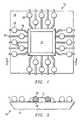
- FIGURE 1 illustrates a first embodiment of an integrated circuit package 10 constructed in accordance with the invention.
- Integrated circuit package 10 comprises package bottom 12, package top 14, lead fingers 16, pads 18 and solder balls 20.
- Package bottom 12 and package top 14 enclose an integrated circuit die (not explicitly shown).
- Package bottom 12 and package top 14 are plastic and can be manufactured using transfer molding technology.
- FIGURE 1 is a bottom view of integrated circuit package 10, and it shows the bottom surface of package top 14.
- Solder balls 20 serve as the terminals for integrated circuit package 10.
- the solder balls 20 are connected to pads 18.
- Pads 18 are conductive, circular in shape, and have a diameter approximately the same as the diameter of one of the solder balls 20.
- Each of the pads 18 is also connected to one of the lead fingers 16.
- Each of the lead fingers 16 is a portion of a lead frame (not explicitly shown) connected to the integrated circuit die (not explicitly shown). Although the pads 18 are connected to the lead fingers 16 in this example, they may be an integral part of the lead fingers 16.
- the lead frame which is comprised of lead fingers 16, is of the type commonly used for plastic packaged integrated circuits.
- the same lead frame previously used in a gull-wing or J-form type circuit can also be used for that die in integrated circuit package 10, except that the lead fingers 16 should be altered such that pads 18 are an integral portion thereof or allow pads 18 to be attached.
- the invention thus allows lead frames presently used for integrated circuits to be quickly modified for use in integrated circuit package 10.
- package bottom 12 is smaller than package top 14.
- Each of the lead fingers 16 comprises a conductive strip electrically connected to the integrated circuit die. Because package bottom 12 does not cover the perimeter of integrated circuit package 10, the portion of each lead finger 16 visible in FIGURE 1 is exposed.
- FIGURE 2 illustrates a cross-sectional view facing in the direction of the arrows labeled "2" in FIGURE 1.
- This cross-sectional view illustrates how each of the lead fingers 16 can be excised and wrapped around package top 14. This configuration helps keep each of the lead fingers 16 in place and prevents them from separating and peeling away from the underside of package top 14.
- the ends of lead fingers 16 bend around the side of package top 14 and substantially conform to its shape. This feature of the invention allows easier component level and subsequent board level electrical testing. Conductors for test connectors can be directly connected to the portion of the lead fingers 16 that bends around the side of package top 14.
- the embodiment of integrated circuit package 10 illustrated in FIGURE 1 may be especially useful in applications where one desires to convert an integrated circuit currently having J-form or gull wing-type leads into a plastic packaged area array integrated circuit.
- the lead fingers 16 can have the same spacing as previously used in the J-form or gull wing package.
- pads 18 are connected to the lead fingers 16 to allow attachment of solder balls 20.
- an electronic appliance manufacturer that seeks to use integrated circuit package 10 in an electronic appliance can make small modifications to the pad placement that was used for the J-form or gull wing version of the integrated circuit package in order to allow use of integrated circuit package 10.
- the invention allows users of integrated circuit package 10 to easily convert circuit boards used with existing J-form or gull wing plastic packaged integrated circuits into boards that can be used with area array plastic packaged integrated circuits such as integrated circuit package 10. Similar advantages can be obtained with the embodiment of integrated circuit package 10 illustrated in FIGURES 3 and 4 below.
- FIGURE 3 illustrates a second embodiment of integrated circuit package 10 constructed in accordance with the invention.
- package bottom 12 has a perimeter substantially the same as the perimeter of package top 14 (not shown in FIGURE 3).
- package bottom 12 has a plurality of openings 22 from which the solder balls 20 protrude. Openings 22 expose a substantially smaller portion of lead fingers 16 than is exposed in the embodiment illustrated in FIGURE 1.
- This embodiment of integrated circuit package 10 also has an integrated circuit die (not explicitly shown) that comprises some type of electronic circuit.
- Package bottom 12 and package top 14 (not explicitly shown in FIGURE 3) form a molded plastic body enclosing the electronic circuit.
- This plastic body has top and bottom surfaces opposing one another that form the major surfaces of the package of integrated circuit package 10.
- Each of the solder balls 20 is electrically connected to one of the pads 18.
- pads 18 may be bonded to lead fingers 16 or may form an integral portion thereof.
- Each of the pads 18 is conductive, adjacent to one of the openings 22, and electrically connected to the integrated circuit die through one of the lead fingers 16.
- Each of the lead fingers 16 forms a portion of the lead frame (not explicitly shown), which is at least partially enclosed by the molded plastic body formed by package bottom 12 and package top 14.
- the lead frame is electrically connected to the integrated circuit die.
- FIGURE 4 illustrates a cross-sectional view of the embodiment of FIGURE 3 facing in the direction of the arrows labeled "4."
- the ends of the lead fingers 16 are excised and wrapped around the side of package top 14. In other words, the ends of lead fingers 16 are wrapped around minor surfaces of integrated circuit package 10. In this embodiment, lead fingers 16 are wrapped around the side of package top 14 for reasons similar to those discussed in connection with FIGURE 2 above.
- Both of the embodiments of integrated circuit package 10 illustrated in FIGURES 1 and 3 can be manufactured using similar processes.
- the integrated circuit die can be connected to the lead frame and packaged using existing transfer molding technology.
- Solder balls 20 may be formed or attached on pads 18 using any known method for creating solder balls 20.
- FIGURES 1-4 use lead fingers 16 comprising part of a lead frame to electrically connect the solder balls 20 to the integrated circuit die.
- Other structures could be used inside of integrated circuit package 10 to connect the solder balls to the integrated circuit die. Examples include flex circuits or laminate circuits. Individual conductors could also be connected directly between the integrated circuit die and the solder balls 20.
- FIGURE 1-4 show how the invention can be used to form a plastic packaged ball grid array.
- the invention can be used for other area array technologies such as column grid arrays or pin grid arrays.
- solder columns would be substituted for solder balls 20.
- conductive pins would be substituted for solder balls 20.
- Solder balls, pins, or solder columns could also be integral portions of the lead frame 16 to which they are attached.
- solder balls 20 are made of solder, they could also be made of another conductive material. The number, spacing, and size of solder balls 20 can also be varied.
- lead fingers 16 are excised and wrapped around package top 14. Alternatively, the lead fingers 16 need not protrude from the side of integrated circuit package 10.
Landscapes
- Lead Frames For Integrated Circuits (AREA)
- Structures Or Materials For Encapsulating Or Coating Semiconductor Devices Or Solid State Devices (AREA)
- Wire Bonding (AREA)
Applications Claiming Priority (2)
| Application Number | Priority Date | Filing Date | Title |
|---|---|---|---|
| US889995P | 1995-12-19 | 1995-12-19 | |
| US8899 | 2001-12-05 |
Publications (2)
| Publication Number | Publication Date |
|---|---|
| EP0780896A2 true EP0780896A2 (fr) | 1997-06-25 |
| EP0780896A3 EP0780896A3 (fr) | 1999-04-14 |
Family
ID=21734333
Family Applications (1)
| Application Number | Title | Priority Date | Filing Date |
|---|---|---|---|
| EP96309224A Withdrawn EP0780896A3 (fr) | 1995-12-19 | 1996-12-18 | Boítier électronique amélioré |
Country Status (6)
| Country | Link |
|---|---|
| US (2) | US5777382A (fr) |
| EP (1) | EP0780896A3 (fr) |
| JP (1) | JPH09191060A (fr) |
| MY (1) | MY128748A (fr) |
| SG (1) | SG52875A1 (fr) |
| TW (1) | TW463276B (fr) |
Cited By (1)
| Publication number | Priority date | Publication date | Assignee | Title |
|---|---|---|---|---|
| EP0874400A1 (fr) * | 1997-04-21 | 1998-10-28 | Oki Electric Industry Co., Ltd. | Dispositif semi-conducteur |
Families Citing this family (30)
| Publication number | Priority date | Publication date | Assignee | Title |
|---|---|---|---|---|
| US5677566A (en) * | 1995-05-08 | 1997-10-14 | Micron Technology, Inc. | Semiconductor chip package |
| JP3793628B2 (ja) * | 1997-01-20 | 2006-07-05 | 沖電気工業株式会社 | 樹脂封止型半導体装置 |
| JP3210881B2 (ja) * | 1997-06-05 | 2001-09-25 | ソニーケミカル株式会社 | Bgaパッケージ基板 |
| US5929522A (en) | 1998-04-17 | 1999-07-27 | Hestia Technologies, Inc. | Semiconductor non-laminate package and method |
| US6635957B2 (en) * | 1998-06-10 | 2003-10-21 | Asat Ltd. | Leadless plastic chip carrier with etch back pad singulation and die attach pad array |
| US7247526B1 (en) | 1998-06-10 | 2007-07-24 | Asat Ltd. | Process for fabricating an integrated circuit package |
| US7271032B1 (en) | 1998-06-10 | 2007-09-18 | Asat Ltd. | Leadless plastic chip carrier with etch back pad singulation |
| US7270867B1 (en) | 1998-06-10 | 2007-09-18 | Asat Ltd. | Leadless plastic chip carrier |
| US7226811B1 (en) | 1998-06-10 | 2007-06-05 | Asat Ltd. | Process for fabricating a leadless plastic chip carrier |
| US8330270B1 (en) | 1998-06-10 | 2012-12-11 | Utac Hong Kong Limited | Integrated circuit package having a plurality of spaced apart pad portions |
| US6933594B2 (en) * | 1998-06-10 | 2005-08-23 | Asat Ltd. | Leadless plastic chip carrier with etch back pad singulation |
| US6872661B1 (en) | 1998-06-10 | 2005-03-29 | Asat Ltd. | Leadless plastic chip carrier with etch back pad singulation and die attach pad array |
| US6229200B1 (en) | 1998-06-10 | 2001-05-08 | Asat Limited | Saw-singulated leadless plastic chip carrier |
| US6989294B1 (en) | 1998-06-10 | 2006-01-24 | Asat, Ltd. | Leadless plastic chip carrier with etch back pad singulation |
| KR20000028360A (ko) * | 1998-10-31 | 2000-05-25 | 김규현 | 반도체 장치 |
| KR100960739B1 (ko) * | 1999-02-26 | 2010-06-01 | 텍사스 인스트루먼츠 인코포레이티드 | 열적으로 향상된 반도체 볼 그리드 어레이 디바이스 및 그제조 방법 |
| US6052045A (en) * | 1999-03-12 | 2000-04-18 | Kearney-National, Inc. | Electromechanical switching device package with controlled impedance environment |
| US6916683B2 (en) * | 2000-05-11 | 2005-07-12 | Micron Technology, Inc. | Methods of fabricating a molded ball grid array |
| USRE38381E1 (en) | 2000-07-21 | 2004-01-13 | Kearney-National Inc. | Inverted board mounted electromechanical device |
| US6391687B1 (en) * | 2000-10-31 | 2002-05-21 | Fairchild Semiconductor Corporation | Column ball grid array package |
| ES2294279T3 (es) * | 2002-03-08 | 2008-04-01 | Kearney-National, Inc. | Rele moldeado de montaje superficial y el metodo de fabricacion del mismo. |
| US7732914B1 (en) | 2002-09-03 | 2010-06-08 | Mclellan Neil | Cavity-type integrated circuit package |
| US7009286B1 (en) | 2004-01-15 | 2006-03-07 | Asat Ltd. | Thin leadless plastic chip carrier |
| US7091581B1 (en) | 2004-06-14 | 2006-08-15 | Asat Limited | Integrated circuit package and process for fabricating the same |
| US7411289B1 (en) | 2004-06-14 | 2008-08-12 | Asat Ltd. | Integrated circuit package with partially exposed contact pads and process for fabricating the same |
| US7595225B1 (en) | 2004-10-05 | 2009-09-29 | Chun Ho Fan | Leadless plastic chip carrier with contact standoff |
| US7358119B2 (en) * | 2005-01-12 | 2008-04-15 | Asat Ltd. | Thin array plastic package without die attach pad and process for fabricating the same |
| US7348663B1 (en) | 2005-07-15 | 2008-03-25 | Asat Ltd. | Integrated circuit package and method for fabricating same |
| US7410830B1 (en) | 2005-09-26 | 2008-08-12 | Asat Ltd | Leadless plastic chip carrier and method of fabricating same |
| US7256481B2 (en) * | 2005-11-30 | 2007-08-14 | Texas Instruments Incorporated | Leadframes for improved moisture reliability and enhanced solderability of semiconductor devices |
Family Cites Families (13)
| Publication number | Priority date | Publication date | Assignee | Title |
|---|---|---|---|---|
| JPS61174752A (ja) * | 1985-01-30 | 1986-08-06 | Seiko Epson Corp | 半導体装置 |
| JPS6332955A (ja) * | 1986-07-25 | 1988-02-12 | Nec Corp | 半導体集積回路装置 |
| US5200362A (en) * | 1989-09-06 | 1993-04-06 | Motorola, Inc. | Method of attaching conductive traces to an encapsulated semiconductor die using a removable transfer film |
| US5293072A (en) * | 1990-06-25 | 1994-03-08 | Fujitsu Limited | Semiconductor device having spherical terminals attached to the lead frame embedded within the package body |
| JPH0462865A (ja) * | 1990-06-25 | 1992-02-27 | Fujitsu Ltd | 半導体装置及びその製造方法 |
| KR940002444B1 (ko) * | 1990-11-13 | 1994-03-24 | 금성일렉트론 주식회사 | 반도체 소자의 패키지 어셈블리 방법 |
| US5157480A (en) * | 1991-02-06 | 1992-10-20 | Motorola, Inc. | Semiconductor device having dual electrical contact sites |
| JPH0563109A (ja) * | 1991-08-29 | 1993-03-12 | New Japan Radio Co Ltd | モールド型icパツケージ |
| JPH05144995A (ja) * | 1991-11-18 | 1993-06-11 | Matsushita Electric Works Ltd | 半導体パツケージ |
| JPH06268101A (ja) * | 1993-03-17 | 1994-09-22 | Hitachi Ltd | 半導体装置及びその製造方法、電子装置、リ−ドフレ−ム並びに実装基板 |
| EP0683517B1 (fr) * | 1994-05-09 | 2002-07-24 | Nec Corporation | Dispositif semi-conducteur ayant une puce semi-conductrice connectée avec une plaque de circuit par des plots de contact et procédé de montage |
| TW359880B (en) * | 1995-08-30 | 1999-06-01 | Samsung Electronics Co Ltd | Method of manufacturing semiconductor chip package |
| US5736432A (en) * | 1996-09-20 | 1998-04-07 | National Semiconductor Corporation | Lead frame with lead finger locking feature and method for making same |
-
1996
- 1996-12-16 MY MYPI96005285A patent/MY128748A/en unknown
- 1996-12-18 EP EP96309224A patent/EP0780896A3/fr not_active Withdrawn
- 1996-12-19 JP JP8339174A patent/JPH09191060A/ja active Pending
- 1996-12-19 SG SG1996011856A patent/SG52875A1/en unknown
- 1996-12-19 US US08/769,917 patent/US5777382A/en not_active Expired - Lifetime
-
1997
- 1997-02-19 TW TW086101926A patent/TW463276B/zh not_active IP Right Cessation
- 1997-08-26 US US08/918,404 patent/US5976914A/en not_active Expired - Lifetime
Non-Patent Citations (1)
| Title |
|---|
| None |
Cited By (2)
| Publication number | Priority date | Publication date | Assignee | Title |
|---|---|---|---|---|
| EP0874400A1 (fr) * | 1997-04-21 | 1998-10-28 | Oki Electric Industry Co., Ltd. | Dispositif semi-conducteur |
| US6084300A (en) * | 1997-04-21 | 2000-07-04 | Oki Electric Industry Co., Ltd. | Compact resin-sealed semiconductor device |
Also Published As
| Publication number | Publication date |
|---|---|
| TW463276B (en) | 2001-11-11 |
| MY128748A (en) | 2007-02-28 |
| JPH09191060A (ja) | 1997-07-22 |
| SG52875A1 (en) | 1998-09-28 |
| US5777382A (en) | 1998-07-07 |
| US5976914A (en) | 1999-11-02 |
| EP0780896A3 (fr) | 1999-04-14 |
Similar Documents
| Publication | Publication Date | Title |
|---|---|---|
| US5976914A (en) | Method of making plastic package for a surface mounted integrated circuit | |
| US5273938A (en) | Method for attaching conductive traces to plural, stacked, encapsulated semiconductor die using a removable transfer film | |
| US4677526A (en) | Plastic pin grid array chip carrier | |
| US5247423A (en) | Stacking three dimensional leadless multi-chip module and method for making the same | |
| US5049973A (en) | Heat sink and multi mount pad lead frame package and method for electrically isolating semiconductor die(s) | |
| US5933710A (en) | Method of providing electrical connection between an integrated circuit die and a printed circuit board | |
| US5467252A (en) | Method for plating using nested plating buses and semiconductor device having the same | |
| US5384689A (en) | Integrated circuit chip including superimposed upper and lower printed circuit boards | |
| US5250841A (en) | Semiconductor device with test-only leads | |
| US5053357A (en) | Method of aligning and mounting an electronic device on a printed circuit board using a flexible substrate having fixed lead arrays thereon | |
| EP0435093A2 (fr) | Dispositif électronique moulé, mince pour le montage en surface | |
| EP1168447A2 (fr) | Dispositif semi- conducteur et methode | |
| JPH0621173A (ja) | 試験専用接点を有する半導体デバイスの製造方法 | |
| KR20010078712A (ko) | 칩 스택 및 그 제조 방법 | |
| US6037662A (en) | Chip scale package | |
| KR20010041593A (ko) | 다수의 반도체 칩을 포함하는 반도체 소자 | |
| KR100226335B1 (ko) | 플라스틱 성형회로 패키지 | |
| JP2001168233A (ja) | 多重回線グリッド・アレイ・パッケージ | |
| JPH01261849A (ja) | 半導体装置の製造方法 | |
| EP0272390A2 (fr) | Empaquetages pour un dispositif semi-conducteur | |
| JP3656861B2 (ja) | 半導体集積回路装置及び半導体集積回路装置の製造方法 | |
| US5849609A (en) | Semiconductor package and a method of manufacturing thereof | |
| JPH06291230A (ja) | 複合半導体装置の製造方法 | |
| KR19980063740A (ko) | 몰딩된 패키지용 다층 리드프레임 | |
| JPH07122701A (ja) | 半導体装置およびその製造方法ならびにpga用リードフレーム |
Legal Events
| Date | Code | Title | Description |
|---|---|---|---|
| PUAI | Public reference made under article 153(3) epc to a published international application that has entered the european phase |
Free format text: ORIGINAL CODE: 0009012 |
|
| AK | Designated contracting states |
Kind code of ref document: A2 Designated state(s): DE FR GB IT NL |
|
| PUAL | Search report despatched |
Free format text: ORIGINAL CODE: 0009013 |
|
| AK | Designated contracting states |
Kind code of ref document: A3 Designated state(s): DE FR GB IT NL |
|
| 17P | Request for examination filed |
Effective date: 19991008 |
|
| 17Q | First examination report despatched |
Effective date: 20030319 |
|
| STAA | Information on the status of an ep patent application or granted ep patent |
Free format text: STATUS: THE APPLICATION IS DEEMED TO BE WITHDRAWN |
|
| 18D | Application deemed to be withdrawn |
Effective date: 20040504 |