EP0783233A2 - Appareil de séparation des composants d'un signal vidéo numérique composite - Google Patents
Appareil de séparation des composants d'un signal vidéo numérique composite Download PDFInfo
- Publication number
- EP0783233A2 EP0783233A2 EP96120719A EP96120719A EP0783233A2 EP 0783233 A2 EP0783233 A2 EP 0783233A2 EP 96120719 A EP96120719 A EP 96120719A EP 96120719 A EP96120719 A EP 96120719A EP 0783233 A2 EP0783233 A2 EP 0783233A2
- Authority
- EP
- European Patent Office
- Prior art keywords
- chrominance component
- component
- separated
- signal
- composite video
- Prior art date
- Legal status (The legal status is an assumption and is not a legal conclusion. Google has not performed a legal analysis and makes no representation as to the accuracy of the status listed.)
- Granted
Links
- 239000002131 composite material Substances 0.000 title claims abstract description 79
- 238000000926 separation method Methods 0.000 claims abstract description 12
- 241000023320 Luma <angiosperm> Species 0.000 claims description 16
- OSWPMRLSEDHDFF-UHFFFAOYSA-N methyl salicylate Chemical compound COC(=O)C1=CC=CC=C1O OSWPMRLSEDHDFF-UHFFFAOYSA-N 0.000 claims description 16
- 230000000295 complement effect Effects 0.000 claims description 4
- 230000009467 reduction Effects 0.000 abstract description 18
- 238000010586 diagram Methods 0.000 description 14
- 238000000034 method Methods 0.000 description 11
- 230000003111 delayed effect Effects 0.000 description 9
- 238000001914 filtration Methods 0.000 description 8
- 230000008859 change Effects 0.000 description 7
- 230000000694 effects Effects 0.000 description 7
- 238000012545 processing Methods 0.000 description 7
- 238000011084 recovery Methods 0.000 description 6
- 230000004044 response Effects 0.000 description 6
- 230000008569 process Effects 0.000 description 4
- 230000006870 function Effects 0.000 description 3
- 230000000737 periodic effect Effects 0.000 description 3
- 238000012546 transfer Methods 0.000 description 3
- 230000005540 biological transmission Effects 0.000 description 2
- 230000001934 delay Effects 0.000 description 2
- 230000004048 modification Effects 0.000 description 2
- 238000012986 modification Methods 0.000 description 2
- 238000013459 approach Methods 0.000 description 1
- 238000006243 chemical reaction Methods 0.000 description 1
- 239000004020 conductor Substances 0.000 description 1
- 230000001419 dependent effect Effects 0.000 description 1
- 238000005070 sampling Methods 0.000 description 1
- 238000001228 spectrum Methods 0.000 description 1
- 230000002123 temporal effect Effects 0.000 description 1
- 230000000007 visual effect Effects 0.000 description 1
Images





Classifications
-
- H—ELECTRICITY
- H04—ELECTRIC COMMUNICATION TECHNIQUE
- H04N—PICTORIAL COMMUNICATION, e.g. TELEVISION
- H04N9/00—Details of colour television systems
- H04N9/77—Circuits for processing the brightness signal and the chrominance signal relative to each other, e.g. adjusting the phase of the brightness signal relative to the colour signal, correcting differential gain or differential phase
- H04N9/78—Circuits for processing the brightness signal and the chrominance signal relative to each other, e.g. adjusting the phase of the brightness signal relative to the colour signal, correcting differential gain or differential phase for separating the brightness signal or the chrominance signal from the colour television signal, e.g. using comb filter
Definitions
- This invention relates to video signal processing in general and in particular to digital apparatus for separating a composite video signal into luminance and chrominance signal components.
- NTSC and PAL television systems it is common practice to combine video luminance (“Y”) and chrominance (“C”) signal components to form a single composite video (“CV”) signal for transmission. After transmission, it is usually necessary to separate the composite video signal into its component parts, luminance and chrominance, for further signal processing.
- Y video luminance
- C chrominance
- An elementary method of separation comprises low-pass filtering a composite video signal to obtain the luminance component and bandpass or high-pass filtering the composite signal to obtain the chrominance component.
- This approach while having the virtue of simplicity, has the disadvantage of not being an efficient form of separation since the composite signal is transmitted with the chrominance component spectrally interleaved with the luminance component.
- Much better separation may be realized by means of comb filtering techniques.
- Such filters exhibit periodic band-pass and band reject characteristics which can efficiently separate the components of a composite signal.
- One method of applying comb filtering comprises comb filtering the composite video signal to obtain a separated chrominance component and then subtracting the separated chrominance component from the composite video signal to obtain the separated luminance component.
- the composite signal is first sampled and converted to digital form.
- the samples are then delayed in a memory and the delayed samples are subtractively combined with the non-delayed samples to produce an output signal which comprises two components.
- One of the components comprises a "vertical detail" component which represents luminance detail in a vertical direction and occupies frequencies below the chrominance signal band.
- the other portion is the desired chrominance signal.
- To obtain only the chrominance signal it is necessary to filter the combed signal to exclude the vertical detail signal component.
- the remaining separated combed chrominance component may be subtractively combined with the composite video signal to obtain the luminance component. Since the luminance component was formed by subtraction of the separated chrominance component, the luminance component will be uncombed below the chrominance band and combed within the chrominance band at locations of the chrominance signal spectra.
- digital composite video signal separators of the general type described may tend to exhibit undesired contouring effects.
- the present invention is directed to meeting a need for a digital composite video signal separator in which such a tendency is reduced.
- Apparatus for separating a luminance component from a composite video input signal comprises a filter responsive to the composite video input signal for providing a separated chrominance component.
- a symmetrical rounding unit is provided for removing a given number of least significant bits of the separated chrominance component to provide a modified chrominance component having a reduced number of bits.
- a combiner combines the composite video signal with the modified chrominance component for providing the separated luminance component.
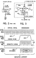
- FIGURE 1 illustrates an exemplary application of a symmetrical "rounding" or “bit reduction” unit 100A embodying the invention in an application for separating a composite video input signal into luminance and chrominance components.
- the composite video signal separator 10 of FIGURE 1 comprises an analog to digital (A/D) converter 14 having an input 12 for receiving an analog composite video input signal to be separated into luminance and chrominance components and having an output for providing a digital composite video (CV) output signal of, illustratively, 8-bits resolution.
- A/D converter sampling rate is equal to four times the frequency of the color subcarrier. Under these conditions there will be 4 sample intervals for one complete color cycle, 2 sample intervals equals one-half of one color cycle and there will be a total of 910 samples per line.
- a drawing convention used in FIGURE 1 is that a 45 degree hash mark drawn through a line and having a number beside it indicates that the line is a bus and the number indicates bus conductors (this also indicates the number of bits per sample).
- the composite video signal CV is applied to a pair of linear digital filters 20 and 30 which produce the chrominance component C from the composite video signal CV.
- the first filter 20 is a one line (1-H) comb filter in which the composite video signal is applied directly to the minuend (+) input 26 of a subtractor 24 and is applied via a one line (1-H) delay (e.g., 910 sample intervals or clock periods) 18 to the subtrahend (-) input 22 of subtractor 24.
- the subtractor produces a combed filter response having the periodic passband response as shown in FIGURE 4A (not to scale).
- the comb response of FIGURE 4A exhibits peaks at odd multiples of one half the horizontal line rate (e.g., Fh/2, 3Fh/2, 5Fh/2, etc.) and exhibits nulls at multiples of the line rate (e.g., Fh, 2Fh, 3Fh, etc.).
- This response recovers two signals from the composite video signal CV.
- the comb output signal comprises mainly chrominance components (C1) substantially free of luminance components.
- the comb output comprises what is commonly called the "vertical detail" component (VD) of the luminance signal.
- VD vertical detail component
- the vertical detail signal component (VD) from the comb filter 20 must be removed.
- VD vertical detail signal component
- FIR finite impulse response
- Filter 30 comprises a first adder 44 having a first input 34 directly coupled to the input 32 and a second input 36 coupled to the input 32 via a series connection of two delay element 40 and 38, each having a delay of two sample intervals. Delay is signified in the drawing by conventional "Z" transform notation in which the negative exponent of "Z" signifies a number of sample interval delays.
- the delayed signal at the common connection of delays 38 and 40 is multiplied by two in multiplier 50 (e.g., a one bit shift) and applied to the subtrahend (-) input of a subtractor 46 which subtracts the delayed and multiplied signal from the output 42 of adder 44.
- multiplier 50 e.g., a one bit shift
- a final stage of filtering in FIR filter 30 is provided by a filter formed by an adder 50 having a first input 52 directly connected to the output of subtractor 46 and having a second input 54 coupled to the output of subtractor 46 via a four sample delay element 56.
- the combination of the first two delay elements 38 and 40 and adder 44 forms a first band pass filter.
- the combination of multiplier 50 and subtractor 46 with the first band pass filter forms a second band pass filter.
- the third filter stage is formed by adder 50 and delay element 56, as previously noted, and all of the filters have poles centered at the chrominance carrier frequency.
- FIGURES 4A-4D illustrate the overall composite video separation process.
- FIGURE 4A illustrates the periodic comb filter response of filter 20 as previously discussed.
- FIGURE 4B illustrates the pass-band of the filter 30 which removes the vertical detail component from the output of filter 20 leaving only the chrominance component as shown in FIGURE 4C.
- this component is subtractively combined with the composite video signal CV to essentially cancel the chrominance component thus leaving only the luminance component as illustrated in FIGURE 4D.
- the signal is subjected to a total of four (4) arithmetic operations.
- the delayed and direct composite video signals were subtracted. This "extends” or increases the number of bits of the resultant difference signal by one bit since it is possible that subtractor 24 may produce a "borrow".
- the combed chrominance signal is 9 bits wide at the subtractor 24 output. This is signified in the drawing by the "hash” line drawn through the output bus of subtractor 24 with the number "9" written beside it. Other signal buses are similarly identified as to the bus "width". Some signals also include an indication of the number of bits concerned.
- the chrominance component is subjected to a total of three arithmetic operations in adders 44 and 50 and subtractor 46.
- Each arithmetic operation adds another bit to the chrominance signal because the operation may produce either a carry (for adders) or a borrow (for subtractors).
- the 8-bit composite video signal applied to comb filter 20 is "extended" to a 9-bit signal after the first subtraction.
- the 9 bit signal becomes 10 bits after the first addition in adder 44.
- the output of adder 44 becomes an 11-bit signal due to the second subtraction in subtractor 46 and finally the fully filtered chrominance signal has extended to 12 bits after the final addition in adder 50.
- the extension of the chrominance signal from 8 bits to 12 bits is similar to having multiplied the chrominance signal by a factor of sixteen (16).
- the "bit-extended" chrominance signal of 12 bits is "bit-reduced" to 10 bits by a 2-bit truncator 60 and converted by a 10 bit D/A converter 62 for application as an analog output signal to output terminal 64.
- Luminance signal recovery requires different chrominance signal processing. Specifically, the technique of bit reduction by simple “truncation” or “chopping off” the lower bits for chroma presents a problem with regard to recovery of the luminance signal component. It has been found that the luminance signal tends to produce undesirable visual artifacts in displayed images when one attempts to reduce the number of chrominance signal bits by simple truncation. It has been found that these artifacts, including contouring, become apparent when displaying images having very low luminance and chrominance spatial gradients. Examples of such signals are discussed later.
- Luminance signal recovery requires reduction of the number of chrominance bits to match the resolution (8-bits) of the composite video signal. This requires reducing the chrominance component from 12 bits to 8 bits without introducing any DC component into the bit reduced signal. This bit reduction is achieved, in accordance with an aspect of the invention, by what is herein termed "symmetrical rounding". It is herein recognized that the processes of symmetrical rounding of the chrominance signal advantageously reduces a tendency toward undesirable contouring in the luminance signal.
- Apparatus to perform an N-bit truncation includes an incrementer, a two input AND gate and an N-input OR gate. Such an arrangement is rather complex but is suitable for use for applying symmetrical rounding in a luma/chroma separation application.
- a preferred symmetrical rounding unit 100A is shown in FIGURE 1.
- Symmetrical bit reduction or rounding in the example of FIGURE 1, is provided by rounding unit 100A.
- an M-bit (e.g., 12-bit) chrominance signal the MSB thereof and an integer K (e.g., 0111 in binary) are added to produce a sum which is truncated by N bits (e.g., 4 bits) to provide a symmetrically rounded or bit reduced digital output signal having "N" fewer least significant bits, LSB's.
- the MSB may be applied in true or complemented form to the adder for selecting wide or narrow rounding modes having different numbers of output zeros disposed about a point of symmetry for a given input signal change.
- undesirable DC shifts due to bit reduction in digital signals are prevented and this has been found to be effective in reducing luminance signal "contouring" as will be described.
- rounding unit 100A comprises a 12 bit full adder 101, a 4 bit truncation unit 103 and a binary number or bias source 102.
- the 12 bit chrominance component provided by filter 30 and a four bit bias number are applied to the addend and augend inputs of adder 101.
- the most significant bit (the sign bit) of the 12 bit chrominance signal is applied to the carry-in input of the 12 bit full adder 101 which, with its carry out, provides a 13 bit chrominance signal.
- the four LSB's of the modified chrominance signal are truncated by a 4-bit truncator 103 thereby producing a 9-bit symmetrically rounded chroma output signal for unit 100A.
- a number is added to the chrominance signal during symmetrical rounding dependent on the polarity of the chrominance signal. If the signal is positive, only the "0111" (decimal “7") value is added and the MSB applied to the carry-in of adder 102 is a zero. For negative numbers, a value of "1000" (decimal "8") is effectively added since the MSB applied to the carry-in of adder 101 will be “1" and will be added with "0111” to the input signal.
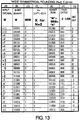
- FIGURE 13 illustrates a case where two bits are to be rounded using the apparatus of unit 100A for signal levels ranging from -11 to +11.
- Column (a) lists the input signal values in decimal.
- Column (b) shows the binary input signal equivalents.
- Column (c) shows the MSB of the binary input signal.
- Column (e) illustrates the output of the adder 101 for the sum of "M", “K” and “MSB” for the input signal from -11 to +11 (decimal).
- the resultant truncated values as shown in columns (f) and (g) range from -3 to +3 and are all symmetrical about zero of the input signal.
- the “step sizes” comprises four identical output values per step above or below the zero level. For symmetry about zero, there are a total of five zeroes that are symmetrically disposed relative to zero of the input signal (hereinafter, the "point of symmetry" or POS).
- unit 100A where 4 LSB's are removed, there is a possibility of a MSB overflow or carry-out and so the total number of bits reduced is 3 so that the 12 bit input signal would be reduced to 9 bits, not the 8 bits ultimately desired. To avoid this condition, the MSB of the output signal of unit 100A is limited by limiter 104.
- the "narrow" mode of symmetrical bit reduction is illustrated in the example of FIGURE 3 by unit 100B and its operation is shown by the table of FIGURE 14.
- the only difference between units 100A and 100B is that in unit 100B the MSB applied to the adder is inverted by inverter 300.
- the effect on the operation of unit 100B is a reduction in the number of output zeroes disposed about the point of symmetry of the input or output signals.
- the narrow mode example, in which the MSB is applied in complemented form (inverted) to the adder there are three zeros produced at the point of symmetry.
- FIGURE 13 the wide mode example, in which the MSB is applied in true (non-inverted form) form to the adder, there are five zeros produced at the point of symmetry as previously noted.
- one has the option of widening or narrowing the zero crossing point" of the symmetrically bit reduced output signal.
- the foregoing rounding-off process may increase the number of bits of the chrominance signal to 13 for the reasons previously explained. This may appear to be opposite to what is needed for extracting the luminance component from the composite video signal CV.
- the round-off circuit since the round-off circuit has effectively moved whatever chrominance information from the lower 4 bits that was useful and placed it in bit 5 and above, it is now possible to truncate the lower 4 bits without significant loss of the chrominance information whereby the luminance contouring effect is substantially reduced.
- the symmetrical bit reduction is provided by adding M, K and the MSB and truncating the sum by a four bit truncator 103.
- This last bit is removed by limiter 104 to produce an 8 bit chrominance output signal.
- the process of limiting after symmetrical rounding does not degrade the contouring performance of the overall system but will facilitate subtraction with the 8 bit composite video signal without having to discard an LSB.
- subtractor 80 which subtracts the 8 bit chrominance signal at its subtrahend input 84 from the composite video signal CV at its minuend input 82.
- the composite signal CV is delayed by 4 sample intervals in delay unit 86.
- the reason for delaying the composite video signal by one full color cycle (4 sample intervals) is to provide temporal alignment with the 12 bit chroma signal which has been delayed by an average of 4 sample intervals in band pass filter 30. Note that "subtraction" in digital circuits is usually performed by means of two's complementing the subtrahend and then performing addition and so the term “subtractively combining" as used herein and in the claims is intended to include such conventional subtraction techniques.
- the arithmetic operation of subtractively combining the composite and chrominance signals produces a separated luminance component with a one bit extension to 9 bits (because of the possibility of a luminance "borrow” result of the subtraction). This extra bit is suppressed by limiting the separated luminance signal Y to 8 bits in limiter 90.
- An analog luminance component output signal is obtained by applying the limited 8 bit luminance component to output terminal 94 via an 8 bit digital to analog (D/A) converter 92.
- FIGURE 5 Five examples of contour sensitive signals are illustrated in FIGURE 5 by the signals labeled "signal one" to "signal five".
- Each signal is a composite video signal taken at the output of A/D converter 14 and having an AC component representing the chrominance at a frequency of the color subcarrier (Fc) and a DC component.
- the DC component represents the luminance component and will be constant for at least several subcarrier cycles.
- the five signal lines illustrate five different steady-state conditions of a luminance signal representing five different but “nearly equal" luminance values in 5 contiguous regions of a displayed video image.
- the analog chroma into A/D converter 14 is selected to be constant, the "digital chroma" at the output of A/D converter may not be because changes in the luma, when added to chroma and quantized, can produce changes in the digital separated chroma.
- FIGURE 6 illustrates the chrominance (C) and vertical detail (VD) components recovered from the output of comb filter 20 for the five lines of composite video of FIGURE 5. These values are steady state values calculated from the equation for "D" (difference) in the heading of FIGURE 6. Specifically, the value of a current C+VD sample equals the value of the present sample minus that of the immediately vertically preceding sample (i.e., the corresponding sample of the previous line). For example, for Signal One the first sample difference for line 2 in FIGURE 6 is equal to the value (+4) of the current sample of Signal One line 2, minus the value of the corresponding previous sample of Signal One in line 1 ("-7") taken from FIGURE 5. All of the C+VD difference values of FIGURE 6 are derived in the same manner from FIGURE 5.
- the next processing step is to remove the unwanted vertical detail from the comb filter 20 output.
- band pass filter 30 having the transfer function for "Pn” shown in the heading of FIGURE 7 for deriving the filtered values of the combed composite signal from the comb values of FIGURE 6.
- the value "Pn” for a current filtered "pixel” of chroma equals the current value (Po) of the corresponding pixel in the table of FIGURE 6, minus 2 times the value two pixels earlier in time , plus 2 times the value 4 pixels ahead, minus 2 times the value six pixels ahead and plus the value eight pixels ahead in time.
- the value of the band pass filtered chrominance signal for Signal One, line 3, pixel 1 is determined as follows.
- the current value is +3, two pixels ahead the value is -3, four pixels ahead (of the current value) the value is +3, six and eight pixels ahead have values of -3 and +3, respectively.
- FIGURE 8 illustrates the effect of "simple" truncation (not symmetrical) of 4 bits from the 12 bit chrominance signal of filter 30.
- FIGURE 9 illustrates the ultimate result on the luminance signal of subtraction of the truncated chroma values of FIGURE 8 from the original composite video values of FIGURE 5.
- substantial contouring results in the luminance signal where "simple" truncation is applied to the chrominance signal.
- the truncated chrominance values using the conventional "simple" truncator 200 of FIGURE 2 are determined by dropping the four least significant bits from the composite video values of FIGURE 7. The results are shown in FIGURE 8.
- FIGURE 9 illustrates the luminance signal levels for the assumed condition of simple truncation of 4 bits from the 12 bit chrominance signal.
- this array there is only one signal that has the correct luminance value, that signal is Signal Three.
- FIGURE 9 is derived by subtracting each truncated chrominance value of FIGURE 8 from the original digital composite video signal values of FIGURE 5. For example, the value of the first luma pixel in FIGURE 5 at line 2 of Signal Three equals the composite video value from FIGURE 5 minus the chrominance value from FIGURE 8. From FIGURE 5 the composite video value CV equals "7". From FIGURE 8 the truncated chrominance value is "-1". Accordingly, for Signal Three, line 2, pixel 1, the luminance signal value equals "6". This is the "correct" value for the luminance signal as explained below.
- every pixel in lines 2 and 3 of Signal Three in FIGURE 7 is either 16 or a multiple thereof (64) so all pixels of Signal Three, lines 2 and 3 are correct.
- the remaining signals all contain chroma errors due to truncation and thus luma errors as well and this can lead to an undesired contouring effect when the components are ultimately displayed.
- Signals One and Five contain the exact same chroma but the luma differs by one count or signal level. Between these two signal levels (6 and 7) there is only one intermediate luma value produced, and that is from Signal Four. This output may be viewed as a luma level of 6.5 (averaged).
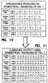
- FIGURES 10 and 11 illustrate the chrominance and luminance separation performance of the present invention and are derived from FIGURES 5, 6 and 7 using essentially the same methods as in FIGURES 8 and 9 except, of course, that here the 12 bit chrominance signal from filter 30 is subjected to symmetrical rounding prior to subtraction from the composite video component rather than being simply truncated. The effects of this treatment of the chrominance signal on the recovered luminance component will now be compared with the truncation example of FIGURE 9.
- the average luminance output shown in FIGURE 11 is always equal to the average of the composite video. This is superior to the simple truncation example of FIGURE 9 which produces an unchanging video signal for several signal regions even though the luminance level (from one signal level to another) is changing. Also, in the example of FIGURE 1, each change in the input steady-state signal value produces a different average luminance output level. Three quarters of the time there is a residual subcarrier Fc component left in the luma but, in general, the appearance of contouring in the example of the invention will be less than that employing straight truncation due to greater luma accuracy for each of the five regions represented by the signals 1-5.
- FIGURE 12 the luma/chroma separation and symmetrical rounding may be implemented with sign/magnitude arithmetic processing.
- source 1200 provides an 8-bit composite video signal S1 in sign/magnitude form to a chrominance filter 1202 which separates the chrominance component producing, illustratively, a 12 bit filtered chrominance signal S2.
- the magnitude bits S3 of this signal are reduced to 8 magnitude bits S8 by symmetrical rounding unit 1204 and to 7 magnitude bits S9 by limiter 1218.
- the sign bit S4 of the 12 bit chroma signal S2 and the 7 magnitude bits S9 are subtracted in subtractor 1208 from the composite video signal S11 (after processing delay 1210) to provide a separated luma output signal S12.
- the rounding unit 1204 in this example operates only on the magnitude bits and comprises an adder 1212 which adds a binary bias signal S6 from source 1214 to the 11 bit chroma magnitude signal S3 to form a 12 bit chroma signal S7.
- the four least significant bits LSB's of signal S7 are truncated by a truncator 1216 and limited by limiter 1218 for application along with the sign bit S4 to the subtractor 1208. Since the four least significant bits of the magnitude signal are symmetrically reduced, the reduction does not introduce a DC component into the resultant signal and so contouring effects in the separated luminance signal are avoided.
- the filtering may be of differing types necessitating rounding off more than four or fewer than four chrominance bits.
- the chrominance filter may be a more comples comb such as a two-line (2-H) comb or a frame comb.
- rejection of the vertical detail output of the comb is illsutrated as being provided by a three stage band pass FIR chrominance signal filter, other suitable filters may be used having more or fewer stages of differing levels of complexity.
- the other chrominance filters may be of the high pass type or a combination of high-pass and band-pass types.
Landscapes
- Engineering & Computer Science (AREA)
- Multimedia (AREA)
- Signal Processing (AREA)
- Processing Of Color Television Signals (AREA)
- Studio Circuits (AREA)
Applications Claiming Priority (2)
| Application Number | Priority Date | Filing Date | Title |
|---|---|---|---|
| US580725 | 1995-12-29 | ||
| US08/580,725 US5633689A (en) | 1995-12-29 | 1995-12-29 | Apparatus for separating a digital composite video signal into components |
Publications (3)
| Publication Number | Publication Date |
|---|---|
| EP0783233A2 true EP0783233A2 (fr) | 1997-07-09 |
| EP0783233A3 EP0783233A3 (fr) | 1997-12-10 |
| EP0783233B1 EP0783233B1 (fr) | 2002-03-13 |
Family
ID=24322278
Family Applications (1)
| Application Number | Title | Priority Date | Filing Date |
|---|---|---|---|
| EP96120719A Expired - Lifetime EP0783233B1 (fr) | 1995-12-29 | 1996-12-21 | Appareil de séparation des composants d'un signal vidéo numérique composite |
Country Status (10)
| Country | Link |
|---|---|
| US (1) | US5633689A (fr) |
| EP (1) | EP0783233B1 (fr) |
| JP (1) | JP3805043B2 (fr) |
| KR (1) | KR100427845B1 (fr) |
| CN (1) | CN1140138C (fr) |
| DE (1) | DE69619786T2 (fr) |
| ES (1) | ES2170191T3 (fr) |
| MX (1) | MX9700195A (fr) |
| MY (1) | MY114574A (fr) |
| SG (1) | SG97750A1 (fr) |
Families Citing this family (6)
| Publication number | Priority date | Publication date | Assignee | Title |
|---|---|---|---|---|
| JPH09215007A (ja) * | 1996-02-01 | 1997-08-15 | Sony Corp | 映像信号処理回路 |
| US5835729A (en) * | 1996-09-13 | 1998-11-10 | Silicon Graphics, Inc. | Circuit to separate and combine color space component data of a video image |
| US7106385B1 (en) * | 1999-12-16 | 2006-09-12 | Thomson Licensing | Apparatus and method for reducing the visual effects of artifacts present in a line scanned video display |
| US20060274819A1 (en) * | 2003-01-30 | 2006-12-07 | Magnus Bengtsson | Truncation and level adjustment of rake output symbols |
| TWI227630B (en) * | 2003-12-22 | 2005-02-01 | Sunplus Technology Co Ltd | A method of inter-frame Y/C separation |
| CN118400505B (zh) * | 2024-06-26 | 2024-10-15 | 浙江芯劢微电子股份有限公司 | 一种抗串扰的复合视频信号yc分离方法和装置 |
Citations (1)
| Publication number | Priority date | Publication date | Assignee | Title |
|---|---|---|---|---|
| US4589084A (en) | 1983-05-16 | 1986-05-13 | Rca Corporation | Apparatus for symmetrically truncating two's complement binary signals as for use with interleaved quadrature signals |
Family Cites Families (12)
| Publication number | Priority date | Publication date | Assignee | Title |
|---|---|---|---|---|
| JPS56153892A (en) * | 1980-04-28 | 1981-11-28 | Sony Corp | Comb type filter |
| US4500912A (en) * | 1982-08-04 | 1985-02-19 | Rca Corporation | FIR Chrominance bandpass sampled data filter with internal decimation |
| US4464675A (en) * | 1982-08-04 | 1984-08-07 | Rca Corporation | Low frequency digital comb filter system |
| US4470069A (en) * | 1982-08-04 | 1984-09-04 | Rca Corporation | Reduced data rate digital comb filter |
| US4556900A (en) * | 1983-05-25 | 1985-12-03 | Rca Corporation | Scaling device as for quantized B-Y signal |
| US4748498A (en) * | 1985-11-19 | 1988-05-31 | Matsushita Electric Industrial Co., Ltd. | Luminance signal processing circuit with recursive filter for reducing noise while retaining a high vertical resolution |
| JPH07121136B2 (ja) * | 1987-06-05 | 1995-12-20 | 日本ビクター株式会社 | 映像信号処理回路 |
| JPH0716253B2 (ja) * | 1987-12-18 | 1995-02-22 | 日本ビクター株式会社 | 適応型輝度信号色信号分離装置 |
| JP3199371B2 (ja) * | 1990-07-30 | 2001-08-20 | 松下電器産業株式会社 | 丸め装置 |
| JPH05265709A (ja) * | 1992-03-23 | 1993-10-15 | Nec Corp | 丸め演算回路 |
| JP3103914B2 (ja) * | 1992-08-21 | 2000-10-30 | ソニー株式会社 | データの丸め処理回路およびデータの復元回路 |
| JP3576573B2 (ja) * | 1993-04-16 | 2004-10-13 | キヤノン株式会社 | 撮像装置 |
-
1995
- 1995-12-29 US US08/580,725 patent/US5633689A/en not_active Expired - Lifetime
-
1996
- 1996-12-18 MY MYPI96005322A patent/MY114574A/en unknown
- 1996-12-21 EP EP96120719A patent/EP0783233B1/fr not_active Expired - Lifetime
- 1996-12-21 DE DE69619786T patent/DE69619786T2/de not_active Expired - Lifetime
- 1996-12-21 ES ES96120719T patent/ES2170191T3/es not_active Expired - Lifetime
- 1996-12-24 SG SG9611911A patent/SG97750A1/en unknown
- 1996-12-26 JP JP34890496A patent/JP3805043B2/ja not_active Expired - Fee Related
- 1996-12-27 KR KR1019960072710A patent/KR100427845B1/ko not_active Expired - Fee Related
- 1996-12-28 CN CNB961167491A patent/CN1140138C/zh not_active Expired - Fee Related
-
1997
- 1997-01-07 MX MX9700195A patent/MX9700195A/es unknown
Patent Citations (1)
| Publication number | Priority date | Publication date | Assignee | Title |
|---|---|---|---|---|
| US4589084A (en) | 1983-05-16 | 1986-05-13 | Rca Corporation | Apparatus for symmetrically truncating two's complement binary signals as for use with interleaved quadrature signals |
Also Published As
| Publication number | Publication date |
|---|---|
| MX9700195A (es) | 1997-12-31 |
| SG97750A1 (en) | 2003-08-20 |
| CN1154622A (zh) | 1997-07-16 |
| ES2170191T3 (es) | 2002-08-01 |
| EP0783233A3 (fr) | 1997-12-10 |
| JP3805043B2 (ja) | 2006-08-02 |
| DE69619786T2 (de) | 2002-08-22 |
| DE69619786D1 (de) | 2002-04-18 |
| MY114574A (en) | 2002-11-30 |
| CN1140138C (zh) | 2004-02-25 |
| US5633689A (en) | 1997-05-27 |
| KR100427845B1 (ko) | 2004-07-27 |
| JPH09200797A (ja) | 1997-07-31 |
| KR970058041A (ko) | 1997-07-31 |
| EP0783233B1 (fr) | 2002-03-13 |
Similar Documents
| Publication | Publication Date | Title |
|---|---|---|
| US5696710A (en) | Apparatus for symmetrically reducing N least significant bits of an M-bit digital signal | |
| KR910004310B1 (ko) | 디지털 필터 | |
| JPS605691A (ja) | デジタルデイザを有するデジタル信号処理装置 | |
| EP0177285B1 (fr) | Système de filtrage adaptatif | |
| US5633689A (en) | Apparatus for separating a digital composite video signal into components | |
| EP0549174A1 (fr) | Commande de filtrage adaptif pour la chrominance | |
| CA1233557A (fr) | Separateur adaptatif de signaux de luminance et de chrominance | |
| JPH07118813B2 (ja) | カラー映像信号エンコード方法 | |
| CA1225144A (fr) | Appareil de traitement lineaire par morceaux de signaux video numeriques | |
| EP0107463B1 (fr) | Système de télévision numérique avec correction d'erreur | |
| EP0122096B1 (fr) | Filtre passe-tout à inversion de chrominance | |
| CN1770879A (zh) | 用于计算由采样信号表示的向量的近似幅度的装置 | |
| JPH0732347B2 (ja) | 巡回形デイジタルフイルタ | |
| KR960011164B1 (ko) | 디매트릭스 연산시 오버플로우/언더플로우 제거회로 | |
| KR950004652Y1 (ko) | 휘도 및 색신호분리장치 | |
| JPS62161210A (ja) | 高速デイジタルフイルタ | |
| JPS60127879A (ja) | アパ−チヤ補正回路 | |
| JPH04119789A (ja) | くし形フィルタ | |
| CN1008046B (zh) | 分段线性数字视频信号处理装置 | |
| JPH04368069A (ja) | ローパスフィルタ | |
| GB2155723A (en) | Digital television system with error correction | |
| JPS6315587A (ja) | Pal輝度信号色信号分離装置 | |
| JPH05257645A (ja) | 加算、減算回路 | |
| JPH02254885A (ja) | 画像信号処理回路 | |
| JPH10290376A (ja) | 画像処理装置 |
Legal Events
| Date | Code | Title | Description |
|---|---|---|---|
| PUAI | Public reference made under article 153(3) epc to a published international application that has entered the european phase |
Free format text: ORIGINAL CODE: 0009012 |
|
| AK | Designated contracting states |
Kind code of ref document: A2 Designated state(s): DE ES FR GB IT |
|
| PUAL | Search report despatched |
Free format text: ORIGINAL CODE: 0009013 |
|
| RHK1 | Main classification (correction) |
Ipc: H04N 1/00 |
|
| AK | Designated contracting states |
Kind code of ref document: A3 Designated state(s): DE ES FR GB IT |
|
| 17P | Request for examination filed |
Effective date: 19980530 |
|
| 17Q | First examination report despatched |
Effective date: 20000808 |
|
| GRAG | Despatch of communication of intention to grant |
Free format text: ORIGINAL CODE: EPIDOS AGRA |
|
| GRAG | Despatch of communication of intention to grant |
Free format text: ORIGINAL CODE: EPIDOS AGRA |
|
| GRAH | Despatch of communication of intention to grant a patent |
Free format text: ORIGINAL CODE: EPIDOS IGRA |
|
| GRAH | Despatch of communication of intention to grant a patent |
Free format text: ORIGINAL CODE: EPIDOS IGRA |
|
| REG | Reference to a national code |
Ref country code: GB Ref legal event code: IF02 |
|
| GRAA | (expected) grant |
Free format text: ORIGINAL CODE: 0009210 |
|
| AK | Designated contracting states |
Kind code of ref document: B1 Designated state(s): DE ES FR GB IT |
|
| REF | Corresponds to: |
Ref document number: 69619786 Country of ref document: DE Date of ref document: 20020418 |
|
| REG | Reference to a national code |
Ref country code: ES Ref legal event code: FG2A Ref document number: 2170191 Country of ref document: ES Kind code of ref document: T3 |
|
| ET | Fr: translation filed | ||
| REG | Reference to a national code |
Ref country code: FR Ref legal event code: D6 |
|
| PLBE | No opposition filed within time limit |
Free format text: ORIGINAL CODE: 0009261 |
|
| STAA | Information on the status of an ep patent application or granted ep patent |
Free format text: STATUS: NO OPPOSITION FILED WITHIN TIME LIMIT |
|
| REG | Reference to a national code |
Ref country code: GB Ref legal event code: 746 Effective date: 20030103 |
|
| 26N | No opposition filed |
Effective date: 20021216 |
|
| PGFP | Annual fee paid to national office [announced via postgrant information from national office to epo] |
Ref country code: ES Payment date: 20080118 Year of fee payment: 12 |
|
| PGFP | Annual fee paid to national office [announced via postgrant information from national office to epo] |
Ref country code: IT Payment date: 20071228 Year of fee payment: 12 |
|
| REG | Reference to a national code |
Ref country code: ES Ref legal event code: FD2A Effective date: 20081222 |
|
| PG25 | Lapsed in a contracting state [announced via postgrant information from national office to epo] |
Ref country code: ES Free format text: LAPSE BECAUSE OF NON-PAYMENT OF DUE FEES Effective date: 20081222 |
|
| REG | Reference to a national code |
Ref country code: DE Ref legal event code: R082 Ref document number: 69619786 Country of ref document: DE Representative=s name: MANFRED ROSSMANITH, DE |
|
| REG | Reference to a national code |
Ref country code: DE Ref legal event code: R082 Ref document number: 69619786 Country of ref document: DE Representative=s name: ROSSMANITH, MANFRED, DIPL.-PHYS. DR.RER.NAT., DE Effective date: 20120724 Ref country code: DE Ref legal event code: R081 Ref document number: 69619786 Country of ref document: DE Owner name: THOMSON LICENSING, FR Free format text: FORMER OWNER: THOMSON CONSUMER ELECTRONICS, INC., INDIANAPOLIS, IND., US Effective date: 20120724 |
|
| PGFP | Annual fee paid to national office [announced via postgrant information from national office to epo] |
Ref country code: GB Payment date: 20121219 Year of fee payment: 17 |
|
| PGFP | Annual fee paid to national office [announced via postgrant information from national office to epo] |
Ref country code: DE Payment date: 20121217 Year of fee payment: 17 Ref country code: FR Payment date: 20130128 Year of fee payment: 17 |
|
| PG25 | Lapsed in a contracting state [announced via postgrant information from national office to epo] |
Ref country code: IT Free format text: LAPSE BECAUSE OF NON-PAYMENT OF DUE FEES Effective date: 20081221 |
|
| REG | Reference to a national code |
Ref country code: DE Ref legal event code: R119 Ref document number: 69619786 Country of ref document: DE |
|
| GBPC | Gb: european patent ceased through non-payment of renewal fee |
Effective date: 20131221 |
|
| REG | Reference to a national code |
Ref country code: FR Ref legal event code: ST Effective date: 20140829 |
|
| REG | Reference to a national code |
Ref country code: DE Ref legal event code: R119 Ref document number: 69619786 Country of ref document: DE Effective date: 20140701 |
|
| PG25 | Lapsed in a contracting state [announced via postgrant information from national office to epo] |
Ref country code: DE Free format text: LAPSE BECAUSE OF NON-PAYMENT OF DUE FEES Effective date: 20140701 |
|
| PG25 | Lapsed in a contracting state [announced via postgrant information from national office to epo] |
Ref country code: FR Free format text: LAPSE BECAUSE OF NON-PAYMENT OF DUE FEES Effective date: 20131231 Ref country code: GB Free format text: LAPSE BECAUSE OF NON-PAYMENT OF DUE FEES Effective date: 20131221 |