EP0786816A2 - Bipolarer Transistor mit einer verbesserten epitaktischen Basiszone und dessen Herstellungsverfahren - Google Patents
Bipolarer Transistor mit einer verbesserten epitaktischen Basiszone und dessen Herstellungsverfahren Download PDFInfo
- Publication number
- EP0786816A2 EP0786816A2 EP97100686A EP97100686A EP0786816A2 EP 0786816 A2 EP0786816 A2 EP 0786816A2 EP 97100686 A EP97100686 A EP 97100686A EP 97100686 A EP97100686 A EP 97100686A EP 0786816 A2 EP0786816 A2 EP 0786816A2
- Authority
- EP
- European Patent Office
- Prior art keywords
- type
- base
- bipolar transistor
- film
- base region
- Prior art date
- Legal status (The legal status is an assumption and is not a legal conclusion. Google has not performed a legal analysis and makes no representation as to the accuracy of the status listed.)
- Granted
Links
- 238000004519 manufacturing process Methods 0.000 title description 24
- 239000010410 layer Substances 0.000 claims abstract description 118
- 238000009413 insulation Methods 0.000 claims abstract description 25
- 239000002356 single layer Substances 0.000 claims abstract description 8
- 238000000034 method Methods 0.000 claims description 83
- 239000012535 impurity Substances 0.000 claims description 21
- 229910000577 Silicon-germanium Inorganic materials 0.000 claims description 2
- 238000009313 farming Methods 0.000 claims 1
- 229910021420 polycrystalline silicon Inorganic materials 0.000 description 73
- 229920005591 polysilicon Polymers 0.000 description 73
- 238000005530 etching Methods 0.000 description 53
- XUIMIQQOPSSXEZ-UHFFFAOYSA-N Silicon Chemical compound [Si] XUIMIQQOPSSXEZ-UHFFFAOYSA-N 0.000 description 39
- 229910052710 silicon Inorganic materials 0.000 description 39
- 239000010703 silicon Substances 0.000 description 39
- 230000008569 process Effects 0.000 description 34
- VYPSYNLAJGMNEJ-UHFFFAOYSA-N Silicium dioxide Chemical compound O=[Si]=O VYPSYNLAJGMNEJ-UHFFFAOYSA-N 0.000 description 28
- 229910052814 silicon oxide Inorganic materials 0.000 description 28
- 238000000206 photolithography Methods 0.000 description 21
- 239000000758 substrate Substances 0.000 description 17
- 239000005368 silicate glass Substances 0.000 description 16
- 239000004065 semiconductor Substances 0.000 description 15
- ZOXJGFHDIHLPTG-UHFFFAOYSA-N Boron Chemical compound [B] ZOXJGFHDIHLPTG-UHFFFAOYSA-N 0.000 description 14
- 229910052796 boron Inorganic materials 0.000 description 14
- 230000015572 biosynthetic process Effects 0.000 description 13
- 230000004888 barrier function Effects 0.000 description 12
- 229910052751 metal Inorganic materials 0.000 description 12
- 239000002184 metal Substances 0.000 description 12
- 229910052581 Si3N4 Inorganic materials 0.000 description 8
- 238000000137 annealing Methods 0.000 description 8
- 238000005229 chemical vapour deposition Methods 0.000 description 8
- 230000009467 reduction Effects 0.000 description 8
- HQVNEWCFYHHQES-UHFFFAOYSA-N silicon nitride Chemical compound N12[Si]34N5[Si]62N3[Si]51N64 HQVNEWCFYHHQES-UHFFFAOYSA-N 0.000 description 8
- 230000006872 improvement Effects 0.000 description 7
- 238000001451 molecular beam epitaxy Methods 0.000 description 7
- 238000009792 diffusion process Methods 0.000 description 6
- 238000005468 ion implantation Methods 0.000 description 6
- 230000004048 modification Effects 0.000 description 6
- 238000012986 modification Methods 0.000 description 6
- 230000002093 peripheral effect Effects 0.000 description 6
- 230000003647 oxidation Effects 0.000 description 5
- 238000007254 oxidation reaction Methods 0.000 description 5
- 239000000126 substance Substances 0.000 description 5
- 230000004913 activation Effects 0.000 description 3
- YZYDPPZYDIRSJT-UHFFFAOYSA-K boron phosphate Chemical compound [B+3].[O-]P([O-])([O-])=O YZYDPPZYDIRSJT-UHFFFAOYSA-K 0.000 description 3
- 229910000149 boron phosphate Inorganic materials 0.000 description 3
- 238000007796 conventional method Methods 0.000 description 3
- 238000003475 lamination Methods 0.000 description 3
- 239000007788 liquid Substances 0.000 description 3
- 238000007747 plating Methods 0.000 description 3
- 101000635799 Homo sapiens Run domain Beclin-1-interacting and cysteine-rich domain-containing protein Proteins 0.000 description 2
- 102100030852 Run domain Beclin-1-interacting and cysteine-rich domain-containing protein Human genes 0.000 description 2
- 230000006866 deterioration Effects 0.000 description 2
- 230000000694 effects Effects 0.000 description 2
- 230000003071 parasitic effect Effects 0.000 description 2
- 239000005365 phosphate glass Substances 0.000 description 2
- ZOKXTWBITQBERF-UHFFFAOYSA-N Molybdenum Chemical compound [Mo] ZOKXTWBITQBERF-UHFFFAOYSA-N 0.000 description 1
- QVGXLLKOCUKJST-UHFFFAOYSA-N atomic oxygen Chemical compound [O] QVGXLLKOCUKJST-UHFFFAOYSA-N 0.000 description 1
- 238000006243 chemical reaction Methods 0.000 description 1
- 239000013078 crystal Substances 0.000 description 1
- 230000008020 evaporation Effects 0.000 description 1
- 238000001704 evaporation Methods 0.000 description 1
- 239000007789 gas Substances 0.000 description 1
- 239000011521 glass Substances 0.000 description 1
- 229910052750 molybdenum Inorganic materials 0.000 description 1
- 239000011733 molybdenum Substances 0.000 description 1
- 239000001301 oxygen Substances 0.000 description 1
- 229910052760 oxygen Inorganic materials 0.000 description 1
- 230000009257 reactivity Effects 0.000 description 1
Images










Classifications
-
- H—ELECTRICITY
- H10—SEMICONDUCTOR DEVICES; ELECTRIC SOLID-STATE DEVICES NOT OTHERWISE PROVIDED FOR
- H10D—INORGANIC ELECTRIC SEMICONDUCTOR DEVICES
- H10D10/00—Bipolar junction transistors [BJT]
- H10D10/01—Manufacture or treatment
- H10D10/051—Manufacture or treatment of vertical BJTs
- H10D10/054—Forming extrinsic base regions on silicon substrate after insulating device isolation in vertical BJTs having single crystalline emitter, collector or base regions
-
- H—ELECTRICITY
- H10—SEMICONDUCTOR DEVICES; ELECTRIC SOLID-STATE DEVICES NOT OTHERWISE PROVIDED FOR
- H10D—INORGANIC ELECTRIC SEMICONDUCTOR DEVICES
- H10D10/00—Bipolar junction transistors [BJT]
- H10D10/40—Vertical BJTs
-
- H—ELECTRICITY
- H10—SEMICONDUCTOR DEVICES; ELECTRIC SOLID-STATE DEVICES NOT OTHERWISE PROVIDED FOR
- H10D—INORGANIC ELECTRIC SEMICONDUCTOR DEVICES
- H10D62/00—Semiconductor bodies, or regions thereof, of devices having potential barriers
- H10D62/10—Shapes, relative sizes or dispositions of the regions of the semiconductor bodies; Shapes of the semiconductor bodies
- H10D62/17—Semiconductor regions connected to electrodes not carrying current to be rectified, amplified or switched, e.g. channel regions
- H10D62/177—Base regions of bipolar transistors, e.g. BJTs or IGBTs
Definitions
- the present invention relates to a semiconductor device and a method of fabricating the same, and more particularly to a bipolar transistor having an improved epitaxial base region and a method of fabricating the same.
- a molecular beam epitaxy system is useful to form a shallow emitter junction so as to reduce a capacitance of the emitter junction as well as reduce an emitter resistance.
- a self-alignment technique is also useful to form the bipolar transistor scaled down.
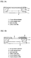
- an n + -type silicon substrate 1 is prepared.
- An n - -type silicon epitaxial layer 2 is formed on the n + -type silicon substrate 1 to form a wafer comprising the n + -type silicon substrate 1 and the n - -type silicon epitaxial layer 2.
- Field oxide films 3 are selectively formed on the wafer by a spot local oxidation of silicon method.
- the field oxide films 3 has a top surface of the same level as the top surface of the n - -type silicon epitaxial layer 2 and a bottom surface of a lower level than the interface between the n + -type silicon substrate 1 and n - -type silicon epitaxial layer 2.
- a surface silicon oxide film 4 is formed which extends over the top surface of the n - -type silicon epitaxial layer 2 and the field oxide films 3.
- p + -type layers 18 are selectively formed in an upper portion of the n - -type silicon epitaxial layer 2 by ion-implantation method.
- the surface silicon oxide film 4 is selectively removed by a photo-lithography method and an anisotropic etching method to selectively leave the surface silicon oxide film 4 over the field oxide films 3 and the vicinity portion of the n - -type silicon epitaxial layer 2 to the field oxide films 3.
- a silicon molecular beam epitaxy system is used to cause a crystal growth of silicon doped with a p-type impurity over an entire surface of the wafer whereby a p-type epitaxial layer 5 is grown over the n - -type silicon epitaxial layer 2 and simultaneously a p-type polysilicon layer 6 is formed over the surface silicon oxide film 4.
- a photo-resist film is applied over the entire surface of the wafer and then patterned by a photo-lithography method to leave a photo-resist film 9j over the p-type epitaxial layer 5 and adjacent portions of the p-type polysilicon layer 6 to the p-type epitaxial layer 5.
- An anisotropic etching is carried out by use of the photo-resist film 9j as a mask to selectively remove the p-type polysilicon layer 6 from the wafer whereby the p-type epitaxial layer 5 and adjacent portions of the p-type polysilicon layer 6 to the p-type epitaxial layer 5 remain over the wafer.
- the photo-resist film 9j is removed from the wafer.
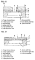
- An insulation film 19 made of silicon oxide or silicon nitride is deposited on an entire surface of the wafer by a chemical vapor deposition method so that the insulation film 19 extends over the p-type epitaxial layer 5, the remaining portions of the p-type polysilicon layer 6 and the surface silicon oxide film 4.
- the insulation film 19 is selectively etched by a photo-lithography method and an anisotropic etching method to form base contact recesses in the insulation film 19 at base contact portions 15 which are positioned over the p + -type layers 18 as well as form an emitter contact recess in the insulation film 19 at an emitter contact portion 22.
- the insulation film 19 has a several tens nanometers.
- the emitter contact recess of the insulation film 19 is further etched by a photo-lithography method and an anisotropic etching method to form an emitter contact hole 22 so that the p-type epitaxial layer 5 is shown via the emitter contact hole 22.
- a polysilicon film 12 is deposited on an entire surface of the wafer by a chemical vapor deposition method so that the polysilicon film 12 extends over the insulation film 19 and within the base recesses and the emitter contact hole of the insulation film 19 whereby the polysilicon film 12 in the emitter contact hole 22 is in contact with the surface of the p-type epitaxial layer 5.
- the polysilicon film 12 is doped with an n-type impurity by an ion implantation before the wafer is subjected to an annealing so as to cause a thermal diffusion of the n-type impurity from the polysilicon film 12 in the emitter contact hole 22 into the p-type epitaxial layer 5 whereby an n-type emitter region 14 is formed in an upper portion of the p-type epitaxial layer 5 wherein this upper portion is a portion which is in contact with the polysilicon film 12 residing in the emitter contact hole 22.
- This annealing process further causes an activation of the p + -type layers 18.
- the polysilicon film 12 is selectively removed by a photo-lithography method and an anisotropic etching method so as to selectively leave the polysilicon film 12 within and around the emitter contact hole 22.
- the insulation film 19 under the base recess portions 15 is farther selectively etched by an anisotropic etching so that base contact holes 15 are formed over the p + -type layers 18 whereby the p + -type layers 18 are shown via the base contact holes 15.
- a barrier metal layer 16 is formed on an entire surface of the wafer by an evaporation so that the barrier metal layer 16 extends over the insulation film 19 and the polysilicon film 12 as well as within the base contact holes 15 whereby the barrier metal layer 16 in the base contact holes 15 is in contact with the p + -type layers 18.
- Electrodes 17 are selectively formed on the barrier metal layer 16 and over the p + -type layers 18 by a photo-lithography method and a plating method wherein the electrodes 17 are defined by a photo-resist pattern not shown in FIG. 1H and formed by that photo-lithography method. After the electrodes 17 have been formed, the photo-resist pattern is removed from the wafer.
- the barrier metal layer 16 is selectively removed by an anisotropic etching method which uses the electrodes 17 as mash so that the barrier metal layer 16 remains only under the electrodes 17 or within and around the base contact boles over the p + -type layers 18. As a result, the bipolar transistor is completed.
- the above conventional method of fabricating the bipolar transistor has the following serious problems with difficulty to form the emitter contact hole 22 and the base recess at the base contact portion 15. Namely, it is required to etch the insulation film 19 with a very small difference in etching depth between the base contact portion 15 and the emitter contact portion 22 as illustrated in FIG. 1E.
- a side etching appears on the insulation film 19, resulting in an undesirable increase in emitter area. This means that the distance of the emitter region from the p + -type layer 18 is shortened whereby a DC property of the bipolar transistor is deteriorated.
- the insulation film 19 under the base recesses 15 has a small thickness, for example, a several tens nanometers.
- This thin portions of the insulation film 19 serve as a protection layer for the base interfaces from the anisotropic etching which is carried out to selectively remove the n-type polysilicon film 12 as described above and also illustrated in FIG. 1G.
- the thickness of the insulation film 19 under the base recesses 15 is likely to be varied slightly due to an unavoidable small variation in depth of the etching.
- the thickness of the insulation film 19 under the base recesses 15 is somewhat reduced from the predetermined value, then there may be raised a problem with over-etching to the insulation film 19 under the base recesses 15 in the process for selectively etching and removing the polysilicon film 12.
- the surface of the p + -type layer 18 may be etched by selectively etching and removing the polysilicon film 12. The etching of the p + -type layer 18 having a high impurity concentration causes the base resistance to be risen, resulting in deterioration in DC property and RF property.
- the above bipolar transistor has a difficulty to reduce the scale thereof for the following reasons. It is essential to provide the p + -type layer 18 as the base plug in the base region. In the light of the issue of an actual discrepancy in alignment to the base contact, it is difficult to reduce the size of the p + -type layer 18 as the base plug formed in the base region. Further, in the lights of the necessity to keep the minimum withstand voltage between the emitter and base as well as of the necessary margin against the discrepancy in alignment and the difficulty to reduce the size of the p + -type layer 18, it is difficult to reduce a distance between the base contact and the emitter contact, for which reason it is difficult to reduce the scale of the base region.
- the p + -type layer 18 extends to a deep level in the collector region. This results in increases in the base-collector junction capacitance. Since it is difficult to reduce the scale of the base region, it is also difficult to reduce the parasitic capacitance. This means that it is difficult to obtain the required shallow junction effects.
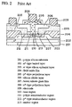
- the conventional bipolar transistor is formed on a p-type silicon substrate 201.
- An n + -type buried layer 202 is formed over the p-type silicon substrate 201.
- An n - -type epitaxial layer 203 is formed over the n + -type buried layer 202.
- the laminations of the p-type silicon substrate 201, the n + -type buried layer 202 and the n - -type epitaxial layer 203 form a wafer.
- Field oxide films 204 are selectively formed on a surface of the n - -type epitaxial layer 203 which surrounds an active region.
- a p-type base region 210 is formed at the center position in the active region of the n - -type epitaxial layer 203.
- a p-type semiconductor region 211 is further provided, which extends to surround the p-type base region 210.
- a p + -type semiconductor region 212 is furthermore provided, which extends to surround the p-type semiconductor region 211.
- An n + -type emitter region 213 is formed over the p-type base region 210.
- a p + -type polysilicon film 205 acting as a base plug lead is formed, which extends over the p + -type semiconductor region 212 and the field oxide films 204.
- Part of the p + -type polysilicon film 205 is in contact with the top surface of the p + -type semiconductor region 212 so that the p + -type polysilicon film 205 is connected via the p + -type semiconductor region 212 and the p-type semiconductor region 211 to the p-type base region 210.
- a boron silicate glass film 207 is formed over the p-type semiconductor region 211 expect over the n + -type emitter region 213.
- a silicon nitride film 206 is further formed, which extends over the boron silicate glass film 207 and part of the p + -type polysilicon film 205.
- an n + -type polysilicon film 208 is formed, which is in contact with the top surface of the n + -type emitter region 213 so that n + -type polysilicon film 208 serves as an emitter plug lead.
- the n + -type polysilicon film 208 serving as the emitter plug lead is electrically isolated by the boron silicate glass film 207 and the silicon nitride film 206 from the p + -type polysilicon film 205 serving as the base plug lead.
- Base electrodes 209 are formed over the p + -type polysilicon film 205 serving as the base plug lead.
- An emitter electrode 209 is also formed over the n + -type polysilicon film 208 serving as the emitter plug lead.
- the above bipolar transistor structure is somewhat suitable for scaling down in the lateral direction of the bipolar transistor as compared to the conventional shallow junction bipolar transistor. Such scaling down in the lateral direction of the bipolar transistor may provide an improvement in the high frequency performance of the bipolar transistor.
- the structure thereof is too complicated and the fabrication processes are also so complicated. Further, there are essential one or more processes to be carried out under a very precise control of the process conditions, for which reason it is difficult to obtain a high yield of the manufacturing of the bipolar transistor.
- it is required to carry out an isotropic etching by use of a liquid chemical or etchant in order to form an over-hang shape.
- It is difficult to precisely control the etching rate of the isotropic etching by use of a liquid chemical or etchant. It is further difficult to suppress variation in the chemical concentration which provides a substantial influence to the etching rate, resulting in variation in the etching rate.
- the variation in the etching rate causes variations in the base resistance and in the distance between the emitter region and the base region whereby it is difficult to obtain a high yield of manufacturing of the bipolar transistor.
- the conventional bipolar transistor is formed on a p-type silicon substrate 301.
- An n + -type buried layer 302 is formed over the p-type silicon substrate 201.
- An n-type well layer 303 is selectively formed in an upper portion of the n + -type buried layer 302.
- Field oxide films 304 are selectively formed on a surface of the wafer to define active regions.
- a p-type base region 310 is formed at a center region in the active region of the n-type well layer 303.
- a p + -type semiconductor region 312 is further provided, which extends to surround the p-type base region 310.
- the p + -type semiconductor region 312 is surrounded by the field oxide film 304.
- An n + -type emitter region 311 is selectively formed in an upper region of the p-type base region 310 so that the n + -type emitter region 311 is separated by the p-type base region 310 from the p + -type semiconductor region 312.
- a p + -type polysilicon film 305 acting as a base plug lead is formed, which extends over the p + -type semiconductor region 312 and the field oxide films 304.
- Part of the p + -type polysilicon film 305 is in contact with the top surface of the p + -type semiconductor region 312 so that the p + -type polysilicon film 305 is connected via the p + -type semiconductor region 312 to the p-type base region 310.
- An n + -type polysilicon film 308 is formed over the wafer which extends to be in contact with the n + -type emitter region 311 so that the n + -type polysilicon film 308 serves as an emitter plug lead as well as extends to be in contact with the n + -type buried layer 302 so that the n + -type polysilicon film 308 serves as a collector plug lead.
- a silicon oxide film 306 is formed, which extends over the p + -type polysilicon film 305 and the n + -type polysilicon film 308.
- a boron phosphate silicate glass film 307 is formed, which extends over the silicon oxide film 306.
- Contact holes are formed in the laminations of the silicon oxide film 306 and the boron phosphate silicate glass film 307.
- Electrodes 309 are formed in the contact holes so that the electrodes 309 are in contact with the n + -type polysilicon films 308 serving as the collector plug lead and the emitter plug lead as well as in contact with the p + -type polysilicon film 305 serving as the base plug lead.
- the above bipolar transistor structure is somewhat suitable for scaling down in the lateral direction of the bipolar transistor as compared to the conventional shallow junction bipolar transistor. Such scaling down in the lateral direction of the bipolar transistor may provide an improvement in the high frequency performance of the bipolar transistor.
- the structure thereof is too complicated and the fabrication processes are also so complicated. Further, there are essential one or more processes to be carried out under a very precise control of the process conditions, for which reason it is difficult to obtain a high yield of the manufacturing of the bipolar transistor.
- a peripheral etching which utilizes a difference in etching reactivity to molybdenum due to a difference in oxygen concentration of the reaction gases.
- the variation in the etching rate causes variations in the base resistance and in the distance between the emitter region and the base region whereby it is difficult to obtain a high yield of manufacturing of the bipolar transistor.
- FIGS. 1A through 1H are fragmentary cross sectional elevation views illustrative of the conventional bipolar transistors with a shallow junction structure, involved in the conventional fabrication method thereof.
- FIG. 2 is a fragmentary cross sectional elevation view illustrative of the conventional bipolar transistor which has been formed by use of a self-alignment technique.
- FIG. 3 is a fragmentary cross sectional elevation view illustrative of the other conventional bipolar transistor which has been formed by use of a self-alignment technique.
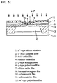
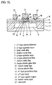
- FIG. 4 is a fragmentary cross sectional elevation view illustrative of a novel bipolar transistor with an improved base region structure in a first embodiment according to the present invention.
- FIGS. 5A through 5L are fragmentary cross sectional elevation views illustrative of a novel bipolar transistor with an improved base region structure in a first embodiment according to the present invention.
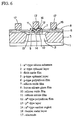
- FIG. 6 is a fragmentary cross sectional elevation view illustrative of a novel bipolar transistor with an improved base region structure in a second embodiment according to the present invention.
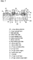
- FIG. 7 is a fragmentary cross sectional elevation view illustrative of a novel bipolar transistor with an improved base region structure in a third embodiment according to the present invention.
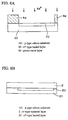
- FIGS. 8A through 8Q are fragmentary cross sectional elevation views illustrative of a novel bipolar transistor with an improved base region structure in a third embodiment according to the present invention.
- FIG. 4 illustrative of a novel bipolar transistor with an improved base region structure
- FIGS. 5A through 5L illustrative of a novel bipolar transistor with an improved base region structure.
- a novel bipolar transistor is formed on an n + -type silicon substrate 1.
- An n - -type epitaxial layer 2 is formed on the n + -type silicon substrate 1. Laminations of the n + -type silicon substrate 1 and the n - -type epitaxial layer 2 form a wafer.
- Field oxide film 3 is selectively formed on a top surface of the n - -type epitaxial layer 2 to define an active region.
- a surface oxide film 4 is formed over the field oxide film 3 and over part of the n - -type epitaxial layer 2.
- the surface oxide film 4 has a base opening which positioned over a base formation region of the n - -type epitaxial layer 2 on which a base layer is formed.
- the n - -type epitaxial layer 2 is shown via the base opening of the surface oxide film 4.
- a p-type epitaxial layer 5 serving as a base region is formed over the n - -type epitaxial layer 2.
- a p-type polysilicon film 6 serving as a base plug layer is formed over the surface oxide film 4.
- the p-type epitaxial layer 5 and the p-type polysilicon film 6 comprises a single layer which has been grown in a single silicon growth process.
- the silicon layer grown over the silicon oxide film is a polysilicon layer whilst the silicon layer grown over the silicon epitaxial layer is a silicon epitaxial layer.
- a silicon oxide film 7 is formed on a peripheral region of the base region 5.
- a boron silicate glass film 8 is formed over the p-type polysilicon film 6.
- the boron silicate glass film 8 has an opening which is positioned over the epitaxial layer 5 as the base region.
- Side wall is formed on the side of the opening wherein the side wall comprises a silicon oxide film 10 and a silicon nitride film 11.
- An n + -type emitter region 14 is formed in an upper region of the epitaxial base layer 5.
- An n + -type polysilicon film 12 is formed on the n + -type emitter region 14 and within the opening.
- a p + -type layer 13 is formed at the boundary region between the epitaxial base layer 5 and the p-type polysilicon film 6.
- the boron silicate glass film 8 has further base contact holes over the p-type polysilicon film 6.
- Base electrodes 17 are formed on barrier metal layers 16 which are formed within the base contact holes and on the p-type polysilicon film 6. Further, An emitter electrode 17 is formed on an emitter barrier metal layer 16 which is formed on the n + -type polysilicon film 12.
- the above epitaxial base layer 5 and the p-type polysilicon film 6 serving as the base plug lead are formed unitary and simultaneously by a molecular beam epitaxy. This makes it possible to precisely control the impurity concentration and the thickness of the epitaxial base layer 5 without any variation thereof. It is easy to obtain or form a shallow junction structure which causes the shallow junction effects.
- the epitaxial base layer 5 and the p-type polysilicon film 6 serving as the base plug lead forms a single layer, for which reason it is not necessary to form any base contact region in the base region. This allows reduction in lateral size of the base region, resulting in a reduction in parasitic capacitance.
- an n - -type epitaxial layer 2 is formed on an n + -type silicon substrate 1 to form a wafer.
- field oxide films 3 are formed for subsequent formation of a surface oxide film 4 by a thermal oxidation of silicon.
- the surface oxide film 4 is selectively removed by a photo-lithography and an anisotropic etching or an isotropic etching to form openings over a base formation region.
- a silicon molecular beam epitaxy system is used to grow a p-type silicon layer wherein the p-type silicon layer over the n - -type epitaxial layer 2 is a p-type epitaxial layer 5 serving as a base region and the p-type silicon layer over the surface silicon oxide film 4 is a p-type polysilicon layer 6.
- the p-type epitaxial layer 5 and the p-type polysilicon layer 6 are unitary and simultaneously.
- a chemical vapor deposition is used o deposit a silicon oxide film 7 for subsequent photo-lithography and an anisotropic etching to leave the silicon oxide film 7 only within the base region.
- a boron silicate glass film 8 is deposited on an entire surface of the wafer.
- a photo-resist film 9a is formed by a photo-lithography method for use as a mask in an anisotropic etching to selectively remove the boron silicate glass film 8 and the silicon oxide film 7 from the emitter region.
- the photo-resist film 9a is then removed before a silicon oxide film 10 is deposited on an entire surface of the wafer by a chemical vapor deposition method.
- an anisotropic etching is used for etch-back to the silicon oxide film 10 so that side wall of the silicon oxide film 10 is formed at the emitter contact portion.
- a silicon nitride film 11 is deposited over an entire surface of the wafer for subsequent etch-back thereto by an anisotropic etching method to form a side wall of the silicon nitride film 11.
- a polysilicon film is deposited by a chemical vapor deposition method for subsequent doping of an n-type impurity by an ion-implantation method at a high impurity concentration to form an n + -type polysilicon film 12.
- an annealing is carried out for activation of the n-type impurity in the n + -type polysilicon film 12 whereby the n-type impurity in the n + -type polysilicon film 12 is diffused into an upper portion of the p-type epitaxial base layer 5 to thereby form an n + -type emitter region 14.
- the boron silicate glass film 8 is made into the same film as the silicon oxide film.
- a diffusion of the p-type impurity into the -type polysilicon film 6 is caused to reduce the sheet resistance of the p-type polysilicon film 6.
- a diffusion of p-type impurity from the p-type polysilicon film 6 is caused whereby a p + -type layer is formed in the base region.
- the polysilicon film 12 is selectively removed by a photo-lithography and an anisotropic etching to form an emitter plug of the polysilicon film 12.
- a photo-resist film 9b is formed by a photo-lithography for subsequent anisotropic etching to selectively remove the boron silicate glass film 8 from the base lead contact portion.
- the polysilicon film 12 is etched before the annealing process is carried out.
- the photo-resist film 9b is removed before a barrier metal film 16 is evaporated on an entire surface of the wafer to form a photo-resist film 9c except on the predetermined electrode formation regions so that electrodes 17 are formed by a plating method.
- the photo-resist film 9c is removed for subsequent anisotropic etching by use of the electrodes 17 as masks to selectively remove the barrier metal layer 16 except under the electrodes whereby the fabrication processes are completed.
- the base region and the base plug lead are unitary and simultaneously formed, for which reason it is not necessary to form a base contact in the base region. This makes it possible to reduce the size of the base region, resulting in an improvement in high frequency performance of the bipolar transistor.
- the base region 5 and the base plug lead are unitary and simultaneously formed and the boron phosphate glass film supplies the -type impurity into the base plug lead 6, resulting in a reduction in the number of the photo-lithography processes as compared to the conventional one. This allows a reduction in the manufacturing cost and time for the bipolar transistor.
- a second embodiment of the present invention will be described with reference to FIG. 6 illustrative of a novel bipolar transistor with an improved base region structure.
- a structural difference of the bipolar transistor of the second embodiment from that of the first embodiment is as follows.
- the field oxide film 3 defines the active region.
- a difference in the fabrication process of the second embodiment from the first embodiment is as follows. In the same manner as in the first embodiment, the field oxide film is formed for subsequent formation of the surface oxide film 4 before an isotropic etching is carried out to remove the surface oxide film 4 from the active region.
- the second embodiment since it is not necessary to carry out a photo-lithography process for formation of the opening on the base formation region, it is possible to reduce the number of the photo-lithography processes. Further, an area of the interface between the collector and the base is reduced, for which reason a collector-base junction capacitance is reduced. Furthermore, it is possible to reduce the capacitance between the collector and the base plug lead, resulting in further improvement in the performance of the bipolar transistor.
- a third embodiment of the present invention will be described with reference to FIG. 7 illustrative of a novel bipolar transistor with an improved base region structure.
- a structural difference of the bipolar transistor of the third embodiment from that of the first embodiment is as follows.
- An n + -type buried layer 20 is formed over a p-type silicon substrate 101.
- An n - -type epitaxial layer 2 serving as a collector region is formed over the n + -type buried layer 20.
- the n + -type buried layer 20 is plugged out to a surface of the substrate via an n + -type collector plug region 21 on which an n + -type polysilicon film 12 is formed.
- FIGS. 8A through 8Q A fabrication method for the above novel bipolar transistor with an improved base region structure will be described with reference to FIGS. 8A through 8Q.
- a photo-resist film 9d is formed to selectively cover a p-type silicon substrate 101 so that the photo-resist film 9d is used as a mask for ion-implantation of n-type impurity to form an n + -type buried layer 20. Otherwise, an insulation film is formed over the substrate except on the active region so that the n + -type buried layer 20 is formed by a thermal diffusion method before the insulation film is removed.
- an n - -type epitaxial layer 2 is grown by a molecular beam epitaxy.
- a field oxide film 3 is formed by a sport local oxidation of silicon method.
- a surface oxide film 4 is formed by a thermal oxidation.
- a photo-resist film 9e is used as a mask for ion-implantation of n-type impurity to form n + -type collector plug region 21.
- the surface oxide film 4 is selectively removed by a photo-lithography and an anisotropic etching to form an opening on the base formation region.
- a p-type epitaxial layer 5 is grown by a silicon molecular beam epitaxy system wherein a p-type epitaxial layer serving as a base region and a p-type polysilicon layer 6 serving as a base plug lead are simultaneously formed over the n - -type epitaxial layer 2 and the surface oxide film 4 respectively.
- a photo-resist film 9f is formed to be used as a mask for an anisotropic etching to selectively remove the p-type polysilicon film 6 in the vicinity of the collector electrode formation region.
- a silicon oxide film 7 is deposited by a chemical vapor deposition method before the silicon oxide film 7 is removed by a photo-lithography and an anisotropic etching to leave the silicon oxide film 7 only within the base region.
- a boron sillate glass film 8 is formed on an entire surface of the wafer.
- the baron silicate glass film 8 and the silicon oxide film 7 are removed from the emitter formation region as well as the boron silicate glass film 8 and the surface oxide film 4 are removed from the collector contact formation region.
- a silicon oxide film 10 is deposited on an entire surface of the wafer by a chemical vapor deposition.
- an etch-back to the silicon oxide film 10 is carried out.
- a side wall of silicon oxide is formed in an peripheral portion and a collector contact peripheral portion.
- a silicon nitride film 11 is deposited on an entire surface of the wafer for subsequent etch-back thereto by use of an anisotropic etching to form the side wall of the silicon nitride film 11 at the peripheral portion of the emitter contact and the peripheral portion of the collector contact.
- a polysilicon film 12 is deposited by a chemical vapor deposition method for subsequent ion-implantation of n-type impurity into the polysilicon film 12.
- an annealing is carried out for activation of the n-type impurity in the n + -type polysilicon film 12 whereby the n-type impurity in the n + -type polysilicon film 12 is diffused into an upper portion of the p-type epitaxial base layer 5 to thereby form an n + -type emitter region 14.
- the boron silicate glass film 8 is made into the same film as the silicon oxide film. Further, a diffusion of the p-type impurity into the -type polysilicon film 6 is caused to reduce the sheet resistance of the p-type polysilicon film 6.
- a diffusion of p-type impurity from the p-type polysilicon film 6 is caused whereby a p + -type layer 13 is formed in the base region.
- the polysilicon film 12 is selectively removed by a photo-lithography and an anisotropic etching to form an emitter plug of the polysilicon film 12.
- a photo-resist film 9h is formed by a photo-lithography for subsequent anisotropic etching to selectively remove the boron silicate glass film 8 from the base lead contact portion.
- the polysilicon film 12 is etched before the annealing process is carried out.
- the photo-resist film 9h is removed before a barrier metal film 16 is evaporated on an entire surface of the wafer to form a photo-resist film 9i except on the predetermined electrode formation regions so that electrodes 17 are formed by a plating method.
- the photo-resist film 9i is removed for subsequent anisotropic etching by use of the electrodes 17 as masks to selectively remove the barrier metal layer 16 except under the electrodes whereby the fabrication processes are completed.
- the base region and the base plug lead are unitary and simultaneously formed, for which reason it is not necessary to form a base contact in the base region. This makes it possible to reduce the size of the base region, resulting in an improvement in high frequency performance of the bipolar transistor.
- the base region 5 and the base plug lead are unitary and simultaneously formed and the baron phosphate glass film supplies the -type impurity into the base plug lead 6, resulting in a reduction in the number of the photo-lithography processes as compared to the conventional one. This allows a reduction in the manufacturing cost and time for the bipolar transistor.
- the base region may be made of SiGe in place of Si in order to obtain a further improvement in the high speed performance.
Landscapes
- Bipolar Transistors (AREA)
Applications Claiming Priority (3)
| Application Number | Priority Date | Filing Date | Title |
|---|---|---|---|
| JP5378/96 | 1996-01-17 | ||
| JP8005378A JP2937253B2 (ja) | 1996-01-17 | 1996-01-17 | 半導体装置およびその製造方法 |
| JP537896 | 1996-01-17 |
Publications (3)
| Publication Number | Publication Date |
|---|---|
| EP0786816A2 true EP0786816A2 (de) | 1997-07-30 |
| EP0786816A3 EP0786816A3 (de) | 1998-01-21 |
| EP0786816B1 EP0786816B1 (de) | 2003-06-18 |
Family
ID=11609515
Family Applications (1)
| Application Number | Title | Priority Date | Filing Date |
|---|---|---|---|
| EP97100686A Expired - Lifetime EP0786816B1 (de) | 1996-01-17 | 1997-01-17 | Bipolarer Transistor mit einer verbesserten epitaktischen Basiszone und dessen Herstellungsverfahren |
Country Status (4)
| Country | Link |
|---|---|
| US (1) | US5789800A (de) |
| EP (1) | EP0786816B1 (de) |
| JP (1) | JP2937253B2 (de) |
| DE (1) | DE69722833T2 (de) |
Cited By (2)
| Publication number | Priority date | Publication date | Assignee | Title |
|---|---|---|---|---|
| DE19842106A1 (de) * | 1998-09-08 | 2000-03-09 | Inst Halbleiterphysik Gmbh | Vertikaler Bipolartransistor und Verfahren zu seiner Herstellung |
| CN100511605C (zh) * | 2002-06-04 | 2009-07-08 | 以爵士半导体公司营业的纽波特有限公司 | 用于双极晶体管中改善的对准容限的方法和有关结构 |
Families Citing this family (11)
| Publication number | Priority date | Publication date | Assignee | Title |
|---|---|---|---|---|
| US6043554A (en) * | 1996-01-25 | 2000-03-28 | Sony Corporation | Bipolar transistor and its manufacturing method |
| US6423990B1 (en) | 1997-09-29 | 2002-07-23 | National Scientific Corporation | Vertical heterojunction bipolar transistor |
| US5912481A (en) | 1997-09-29 | 1999-06-15 | National Scientific Corp. | Heterojunction bipolar transistor having wide bandgap, low interdiffusion base-emitter junction |
| US6967144B1 (en) | 2001-06-20 | 2005-11-22 | National Semiconductor Corporation | Low doped base spacer for reduction of emitter-base capacitance in bipolar transistors with selectively grown epitaxial base |
| US6867477B2 (en) * | 2002-11-07 | 2005-03-15 | Newport Fab, Llc | High gain bipolar transistor |
| US6960820B2 (en) * | 2003-07-01 | 2005-11-01 | International Business Machines Corporation | Bipolar transistor self-alignment with raised extrinsic base extension and methods of forming same |
| US7002221B2 (en) * | 2003-08-29 | 2006-02-21 | International Business Machines Corporation | Bipolar transistor having raised extrinsic base with selectable self-alignment and methods of forming same |
| US9412758B2 (en) * | 2007-12-10 | 2016-08-09 | Newport Fab, Llc | Semiconductor on insulator (SOI) structure with more predictable junction capacitance and method for fabrication |
| US9041149B2 (en) * | 2008-08-19 | 2015-05-26 | Nxp, B.V. | Gringo heterojunction bipolar transistor with a metal extrinsic base region |
| JP2010251368A (ja) * | 2009-04-10 | 2010-11-04 | Renesas Electronics Corp | バイポーラトランジスタ及びその製造方法 |
| US8716096B2 (en) | 2011-12-13 | 2014-05-06 | International Business Machines Corporation | Self-aligned emitter-base in advanced BiCMOS technology |
Citations (2)
| Publication number | Priority date | Publication date | Assignee | Title |
|---|---|---|---|---|
| JPS61290761A (ja) | 1985-06-19 | 1986-12-20 | Matsushita Electric Ind Co Ltd | 半導体装置の製造方法 |
| JPH05315347A (ja) | 1992-05-12 | 1993-11-26 | Oki Electric Ind Co Ltd | バイポーラトランジスタの製造方法 |
Family Cites Families (8)
| Publication number | Priority date | Publication date | Assignee | Title |
|---|---|---|---|---|
| US3600651A (en) * | 1969-12-08 | 1971-08-17 | Fairchild Camera Instr Co | Bipolar and field-effect transistor using polycrystalline epitaxial deposited silicon |
| US5391503A (en) * | 1991-05-13 | 1995-02-21 | Sony Corporation | Method of forming a stacked semiconductor device wherein semiconductor layers and insulating films are sequentially stacked and forming openings through such films and etchings using one of the insulating films as a mask |
| JP2655052B2 (ja) * | 1993-10-07 | 1997-09-17 | 日本電気株式会社 | 半導体装置およびその製造方法 |
| JPH07193075A (ja) * | 1993-12-27 | 1995-07-28 | Nec Corp | 半導体装置およびその製造方法 |
| US5436180A (en) * | 1994-02-28 | 1995-07-25 | Motorola, Inc. | Method for reducing base resistance in epitaxial-based bipolar transistor |
| JP2970425B2 (ja) * | 1994-09-26 | 1999-11-02 | 日本電気株式会社 | バイポーラトランジスタの製造方法 |
| US5616508A (en) * | 1995-01-09 | 1997-04-01 | Texas Instruments Incorporated | High speed bipolar transistor using a patterned etch stop and diffusion source |
| JPH09167777A (ja) * | 1995-12-15 | 1997-06-24 | Toshiba Corp | 半導体装置及びその製造方法 |
-
1996
- 1996-01-17 JP JP8005378A patent/JP2937253B2/ja not_active Expired - Lifetime
-
1997
- 1997-01-17 US US08/785,611 patent/US5789800A/en not_active Expired - Lifetime
- 1997-01-17 DE DE69722833T patent/DE69722833T2/de not_active Expired - Lifetime
- 1997-01-17 EP EP97100686A patent/EP0786816B1/de not_active Expired - Lifetime
Patent Citations (2)
| Publication number | Priority date | Publication date | Assignee | Title |
|---|---|---|---|---|
| JPS61290761A (ja) | 1985-06-19 | 1986-12-20 | Matsushita Electric Ind Co Ltd | 半導体装置の製造方法 |
| JPH05315347A (ja) | 1992-05-12 | 1993-11-26 | Oki Electric Ind Co Ltd | バイポーラトランジスタの製造方法 |
Cited By (3)
| Publication number | Priority date | Publication date | Assignee | Title |
|---|---|---|---|---|
| DE19842106A1 (de) * | 1998-09-08 | 2000-03-09 | Inst Halbleiterphysik Gmbh | Vertikaler Bipolartransistor und Verfahren zu seiner Herstellung |
| US6627972B1 (en) | 1998-09-08 | 2003-09-30 | Institut Fuer Halbleiterphysik Frankfurt (Oder) Gmbh | Vertical bipolar transistor |
| CN100511605C (zh) * | 2002-06-04 | 2009-07-08 | 以爵士半导体公司营业的纽波特有限公司 | 用于双极晶体管中改善的对准容限的方法和有关结构 |
Also Published As
| Publication number | Publication date |
|---|---|
| JP2937253B2 (ja) | 1999-08-23 |
| US5789800A (en) | 1998-08-04 |
| EP0786816A3 (de) | 1998-01-21 |
| JPH09199510A (ja) | 1997-07-31 |
| DE69722833T2 (de) | 2004-05-06 |
| DE69722833D1 (de) | 2003-07-24 |
| EP0786816B1 (de) | 2003-06-18 |
Similar Documents
| Publication | Publication Date | Title |
|---|---|---|
| US4252582A (en) | Self aligned method for making bipolar transistor having minimum base to emitter contact spacing | |
| US4318751A (en) | Self-aligned process for providing an improved high performance bipolar transistor | |
| US5024957A (en) | Method of fabricating a bipolar transistor with ultra-thin epitaxial base | |
| US4916083A (en) | High performance sidewall emitter transistor | |
| US5382828A (en) | Triple self-aligned bipolar junction transistor | |
| US5101256A (en) | Bipolar transistor with ultra-thin epitaxial base and method of fabricating same | |
| US4641416A (en) | Method of making an integrated circuit structure with self-aligned oxidation to isolate extrinsic base from emitter | |
| EP0061729A2 (de) | Verfahren zur Herstellung von Strukturen mit integrierten Halbleiterkomponenten mit Mesa-Konfiguration und Struktur diesen Typs | |
| EP0350610A2 (de) | Herstellungsverfahren eines Bipolartransistors mit selbstjustierter Emitter-Basis unter Benutzung selektiver und nichtselektiver Epitaxie | |
| US4703554A (en) | Technique for fabricating a sidewall base contact with extrinsic base-on-insulator | |
| JPH03171632A (ja) | トランジスタ及びその製造方法 | |
| US5789800A (en) | Bipolar transistor having an improved epitaxial base region | |
| US4997775A (en) | Method for forming a complementary bipolar transistor structure including a self-aligned vertical PNP transistor | |
| US5194926A (en) | Semiconductor device having an inverse-T bipolar transistor | |
| US5677209A (en) | Method for fabricating a vertical bipolar transistor | |
| EP0372476A2 (de) | Halbleiteranordnung mit veminderter parasitischer Kapazität und Verfahren zu ihrer Herstellung | |
| JPH05206151A (ja) | 半導体装置 | |
| EP0290763B1 (de) | Hochleistungstransistor mit Seitenwandemitter | |
| US5286661A (en) | Method of forming a bipolar transistor having an emitter overhang | |
| EP0026276B1 (de) | Verfahren zur Herstellung fadenförmiger Sockeltransistoren | |
| US6080631A (en) | Method for manufacturing self-alignment type bipolar transistor having epitaxial base layer | |
| JPH0241170B2 (de) | ||
| US5198375A (en) | Method for forming a bipolar transistor structure | |
| US5147809A (en) | Method of producing a bipolar transistor with a laterally graded emitter (LGE) employing a refill method of polycrystalline silicon | |
| US5523614A (en) | Bipolar transistor having enhanced high speed operation through reduced base leakage current |
Legal Events
| Date | Code | Title | Description |
|---|---|---|---|
| PUAI | Public reference made under article 153(3) epc to a published international application that has entered the european phase |
Free format text: ORIGINAL CODE: 0009012 |
|
| AK | Designated contracting states |
Kind code of ref document: A2 Designated state(s): DE NL |
|
| PUAL | Search report despatched |
Free format text: ORIGINAL CODE: 0009013 |
|
| AK | Designated contracting states |
Kind code of ref document: A3 Designated state(s): DE NL |
|
| 17P | Request for examination filed |
Effective date: 19971208 |
|
| 17Q | First examination report despatched |
Effective date: 19990924 |
|
| GRAH | Despatch of communication of intention to grant a patent |
Free format text: ORIGINAL CODE: EPIDOS IGRA |
|
| RAP1 | Party data changed (applicant data changed or rights of an application transferred) |
Owner name: NEC COMPOUND SEMICONDUCTOR DEVICES, LTD. |
|
| GRAH | Despatch of communication of intention to grant a patent |
Free format text: ORIGINAL CODE: EPIDOS IGRA |
|
| GRAA | (expected) grant |
Free format text: ORIGINAL CODE: 0009210 |
|
| AK | Designated contracting states |
Designated state(s): DE NL |
|
| REF | Corresponds to: |
Ref document number: 69722833 Country of ref document: DE Date of ref document: 20030724 Kind code of ref document: P |
|
| PLBE | No opposition filed within time limit |
Free format text: ORIGINAL CODE: 0009261 |
|
| STAA | Information on the status of an ep patent application or granted ep patent |
Free format text: STATUS: NO OPPOSITION FILED WITHIN TIME LIMIT |
|
| 26N | No opposition filed |
Effective date: 20040319 |
|
| PGFP | Annual fee paid to national office [announced via postgrant information from national office to epo] |
Ref country code: NL Payment date: 20060115 Year of fee payment: 10 |
|
| NLV4 | Nl: lapsed or anulled due to non-payment of the annual fee |
Effective date: 20070801 |
|
| PG25 | Lapsed in a contracting state [announced via postgrant information from national office to epo] |
Ref country code: NL Free format text: LAPSE BECAUSE OF NON-PAYMENT OF DUE FEES Effective date: 20070801 |
|
| REG | Reference to a national code |
Ref country code: DE Ref legal event code: R082 Ref document number: 69722833 Country of ref document: DE Representative=s name: GLAWE DELFS MOLL - PARTNERSCHAFT VON PATENT- U, DE |
|
| REG | Reference to a national code |
Ref country code: DE Ref legal event code: R082 Ref document number: 69722833 Country of ref document: DE Representative=s name: GLAWE DELFS MOLL PARTNERSCHAFT MBB VON PATENT-, DE Effective date: 20120828 Ref country code: DE Ref legal event code: R082 Ref document number: 69722833 Country of ref document: DE Representative=s name: GLAWE DELFS MOLL - PARTNERSCHAFT VON PATENT- U, DE Effective date: 20120828 Ref country code: DE Ref legal event code: R081 Ref document number: 69722833 Country of ref document: DE Owner name: TESSERA ADVANCED TECHNOLOGIES, INC., SAN JOSE, US Free format text: FORMER OWNER: NEC ELECTRONICS CORP., KAWASAKI, KANAGAWA, JP Effective date: 20120828 Ref country code: DE Ref legal event code: R081 Ref document number: 69722833 Country of ref document: DE Owner name: RENESAS ELECTRONICS CORPORATION, JP Free format text: FORMER OWNER: NEC ELECTRONICS CORP., KAWASAKI, JP Effective date: 20120828 |
|
| REG | Reference to a national code |
Ref country code: DE Ref legal event code: R082 Ref document number: 69722833 Country of ref document: DE Representative=s name: GLAWE DELFS MOLL PARTNERSCHAFT MBB VON PATENT-, DE |
|
| REG | Reference to a national code |
Ref country code: DE Ref legal event code: R082 Ref document number: 69722833 Country of ref document: DE Representative=s name: GLAWE DELFS MOLL PARTNERSCHAFT MBB VON PATENT-, DE Effective date: 20140829 Ref country code: DE Ref legal event code: R081 Ref document number: 69722833 Country of ref document: DE Owner name: TESSERA ADVANCED TECHNOLOGIES, INC., SAN JOSE, US Free format text: FORMER OWNER: RENESAS ELECTRONICS CORPORATION, KAWASAKI-SHI, KANAGAWA, JP Effective date: 20140829 |
|
| PGFP | Annual fee paid to national office [announced via postgrant information from national office to epo] |
Ref country code: DE Payment date: 20160127 Year of fee payment: 20 |
|
| REG | Reference to a national code |
Ref country code: DE Ref legal event code: R071 Ref document number: 69722833 Country of ref document: DE |