EP0788143B1 - Méthode de production d'un composant à semi-conducteur et emploi d'un agent de rinçage pour le nettoyage de dispositif semi-conducteur - Google Patents
Méthode de production d'un composant à semi-conducteur et emploi d'un agent de rinçage pour le nettoyage de dispositif semi-conducteur Download PDFInfo
- Publication number
- EP0788143B1 EP0788143B1 EP97100935A EP97100935A EP0788143B1 EP 0788143 B1 EP0788143 B1 EP 0788143B1 EP 97100935 A EP97100935 A EP 97100935A EP 97100935 A EP97100935 A EP 97100935A EP 0788143 B1 EP0788143 B1 EP 0788143B1
- Authority
- EP
- European Patent Office
- Prior art keywords
- semiconductor device
- photoresist
- producing
- rinse
- remover
- Prior art date
- Legal status (The legal status is an assumption and is not a legal conclusion. Google has not performed a legal analysis and makes no representation as to the accuracy of the status listed.)
- Expired - Lifetime
Links
Images
Classifications
-
- H—ELECTRICITY
- H10—SEMICONDUCTOR DEVICES; ELECTRIC SOLID-STATE DEVICES NOT OTHERWISE PROVIDED FOR
- H10P—GENERIC PROCESSES OR APPARATUS FOR THE MANUFACTURE OR TREATMENT OF DEVICES COVERED BY CLASS H10
- H10P52/00—Grinding, lapping or polishing of wafers, substrates or parts of devices
-
- H—ELECTRICITY
- H10—SEMICONDUCTOR DEVICES; ELECTRIC SOLID-STATE DEVICES NOT OTHERWISE PROVIDED FOR
- H10P—GENERIC PROCESSES OR APPARATUS FOR THE MANUFACTURE OR TREATMENT OF DEVICES COVERED BY CLASS H10
- H10P70/00—Cleaning of wafers, substrates or parts of devices
- H10P70/20—Cleaning during device manufacture
- H10P70/27—Cleaning during device manufacture during, before or after processing of conductive materials, e.g. polysilicon or amorphous silicon layers
- H10P70/273—Cleaning during device manufacture during, before or after processing of conductive materials, e.g. polysilicon or amorphous silicon layers the processing being a delineation of conductive layers, e.g. by RIE
-
- G—PHYSICS
- G03—PHOTOGRAPHY; CINEMATOGRAPHY; ANALOGOUS TECHNIQUES USING WAVES OTHER THAN OPTICAL WAVES; ELECTROGRAPHY; HOLOGRAPHY
- G03F—PHOTOMECHANICAL PRODUCTION OF TEXTURED OR PATTERNED SURFACES, e.g. FOR PRINTING, FOR PROCESSING OF SEMICONDUCTOR DEVICES; MATERIALS THEREFOR; ORIGINALS THEREFOR; APPARATUS SPECIALLY ADAPTED THEREFOR
- G03F7/00—Photomechanical, e.g. photolithographic, production of textured or patterned surfaces, e.g. printing surfaces; Materials therefor, e.g. comprising photoresists; Apparatus specially adapted therefor
- G03F7/26—Processing photosensitive materials; Apparatus therefor
- G03F7/42—Stripping or agents therefor
- G03F7/422—Stripping or agents therefor using liquids only
- G03F7/423—Stripping or agents therefor using liquids only containing mineral acids or salts thereof, containing mineral oxidizing substances, e.g. peroxy compounds
-
- Y—GENERAL TAGGING OF NEW TECHNOLOGICAL DEVELOPMENTS; GENERAL TAGGING OF CROSS-SECTIONAL TECHNOLOGIES SPANNING OVER SEVERAL SECTIONS OF THE IPC; TECHNICAL SUBJECTS COVERED BY FORMER USPC CROSS-REFERENCE ART COLLECTIONS [XRACs] AND DIGESTS
- Y10—TECHNICAL SUBJECTS COVERED BY FORMER USPC
- Y10S—TECHNICAL SUBJECTS COVERED BY FORMER USPC CROSS-REFERENCE ART COLLECTIONS [XRACs] AND DIGESTS
- Y10S438/00—Semiconductor device manufacturing: process
- Y10S438/906—Cleaning of wafer as interim step
Definitions
- the present invention relates to a cleaning method in a process of producing semiconductor integrated circuits having a conductive metal film on a semiconductor wafer, wherein cleaning is carried out after the removal of a photoresist with a removing agent, and to a rinse for cleaning semiconductor devices that will be used in the above cleaning.
- a conductive film for a metal wiring material is formed on a semiconductor wafer by such a technique as sputtering and CVD. Then, a photoresist is applied to the conductive film and is exposed and developed by photolithography to form a pattern and the unmasked portion of the conductive film are dry-etched with a reactive gas with the photoresist allowed to serve as a mask thereby forming a fine wiring.
- the acid removers are weak in removing power and are strong in corrosive action on conductive metal films used for fine wiring processing, they are not so often used in recent fine wiring processing wherein strict dimensional accuracy is required.
- the aqueous solution remover (1) comprising a quaternary ammonium hydroxide as a main agent greatly corrodes the conductive metal film of aluminum, an aluminum alloy, titanium, tungsten or the like as a wiring material and the corrosive action thereof is further accelerated in the case wherein pure water or ultrapure water is used as a rinse, leading to the problem that a phenomenon of corrosion in the form of numerous pits or craters takes place on the metal surface.
- the remover (2) comprising an alkanolamine as a main agent
- an alcohol such as methanol and propanol
- rinsing is carried out using pure water or ultrapure water. If the cleaning with an alcohol is not carried out satisfactorily, corrosion of the conductive metal film takes place in the subsequent cleaning with pure water or ultrapure water, leading to a phenomenon of corrosion in the form of pits or craters.
- an alkanolamine is used as a main agent and a reducing substance, such as a hydroxylamine, is used as an auxiliary.
- a reducing substance such as a hydroxylamine
- cleaning with an organic solvent, such as an alcohol, as a rinse is carried out and then cleaning with pure water or ultrapure water as a rinse is carried out.
- cleaning with pure water or ultrapure water as a rinse is directly carried out without using an organic solvent, such as an alcohol.
- an organic solvent such as an alcohol
- Japanese Patent Application Laid-Open No. 184595/1994 discloses that after a basic remover is used, cleaning with a hydroxycarboxylate solvent, an alkoxycarboxylic acid solvent, an amide solvent, a lactone solvent, a sulfur compound solvent, or the like as a rinse instead of an alcohol is carried out and then cleaning with pure water or ultrapure water as a rinse is carried out.
- the same problem as that in the cases of the removers (2) and (3) is brought about, and with respect to a phenomenon of corrosion of aluminum or the like, no improvements have been achieved.
- a flammable hazardous material such as an alcohol
- any countermeasures cannot be found against corrosion in the form of craters or pits which is caused when pure water or ultrapure water is used. Therefore, it is desired to develop a safe cleaning method wherein a phenomenon of corrosion of conductive metal films is not noted.
- a protective deposited film that is a reaction product of a reactive gas with the resist is formed. If this protective deposited film is left, it causes breakage of wires or abnormal wiring, leading to various troubles. Therefore, it is desired to remove the protective deposited film completely.
- acid or basic organic removing agents are conventionally used generally, these removing agents are not suitable for recent ultrafine wiring processing wherein dimensional accuracy is strict because these removing agents are accompanied by such defects that they are used at high remove temperatures or are highly dangerous because of their flash points and corrode the conductive film of a metal used in ultrafine wiring processing.
- an object of the present invention is to provide a method of producing a semiconductor device wherein a photoresist film applied to a conductive metal film formed on a semiconductor wafer, a photoresist layer remaining after etching, any resist residue (protective deposited film or side wall protective film) remaining after etching followed by ashing, or the like is removed with a remover, which method can produce a highly accurate circuital wiring by carrying out the removal and cleaning in a safe and simple manner without corroding the conductive metal film at all.
- the inventors of the present invention have found that, according to a method wherein a photoresist film on a conductive metal film, a photoresist film after dry-etching, or any resist residue remaining after dry-etching followed by ashing is removed with a remover and washing with a rinse of pure water or ultrapure water containing a peroxide is carried out, the conductive metal film is not corroded at all and a highly accurate circuital wiring can be produced safely since a highly dangerous organic solvent, such as an alcohol, is not used.
- the inventors of the present invention have found that it is suitable that after a mask of a photoresist is formed on a conductive metal film (a photolithographic process or the like), for the formation of a wiring structure by dry-etching the unmasked portion, the protective deposited film (also referred to as resist residue or side wall protective film) occurring on the side wall sections of the photoresist and the conductive film is removed with a removing agent containing a fluorine compound followed by cleaning with a rinse comprising ultrapure water or pure water containing a peroxide.
- the present invention provides a method of producing a semiconductor device, comprising cleaning with a rinse in the form of water containing a peroxide after removal of a photoresist with a removing agent in the course of removal of the photoresist applied to a conductive metal film formed on a semiconductor wafer.
- the present invention provides the use of a rinse for cleaning a semiconductor device, the rinse comprising water that contains 0.1 to 30 % of one or more peroxides selected from among hydrogen peroxide, benzoyl peroxide, dialkyl peroxides, hydroperoxides, and peracids.
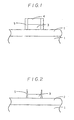
- Fig. 1 shows a cross section of a semiconductor device formed with an aluminum wiring body (Al-Si-Cu layer) by dry-etching with a photoresist film used as a mask.
- Fig. 2 shows a cross section of the semiconductor device of Fig. 1 wherein the photoresist film was removed by ashing the resist using oxygen plasma.
- 1 indicates a semiconductor substrate
- 2 indicates an oxide film (SiO 2 )
- 3 indicates an aluminum wiring body (Al-Si-Cu layer)
- 4 indicates a photoresist film
- 5 indicates a side wall protective film (photoresist residue).
- the conductive metal film to be formed on a semiconductor wafer is not particularly restricted and preferably is made of aluminum, an aluminum alloy, titanium or a tungsten alloy.
- the photoresist that will be removed with a removing agent includes, for example, a photoresist on the conductive film, a photoresist layer after dry-etching, or any resist residue remaining after dry-etching followed by ashing.
- a side wall protective film or a protective deposited film In passing said resist residue is also referred to as a side wall protective film or a protective deposited film and such a protective deposited film is produced as a product of a reaction of a reactive gas with a resist on a conductive film and the side wall sections of a photoresist when a photoresist is applied to a conductive film, a mask is formed by photolithography, and a wiring structure is formed by dry-etching the unmasked portions followed by ashing.
- a basic remover can be mentioned such as those described in the description of the prior art, i.e., (1) an aqueous solution remover comprising a quaternary ammonium hydroxide as a main agent, (2) a remover comprising an alkanolamine as a main agent, and (3) a remover comprising an alkanolamine as a main agent and a reducing agent as an auxiliary, but the present invention is not limited to them, and any of aqueous or non-aqueous basic removers can be used.
- a remover that contains a fluorine compound can be mentioned as a removing agent preferably used to remove the protective deposited film.
- a remover that contains a fluorine compound is not particularly restricted as long as it is a removing agent that contains a fluorine compound, such as hydrofluoric acid, ammonium fluoride, and ammonium hydrogenfluoride.
- Use can be made of any of all removing agents containing a fluorine compound, which can be in the form of an aqueous or non-aqueous solution to which an anticorrosive agent or an organic solvent has been added.
- water containing a peroxide is used as a rinse.
- pure water or ultrapure water is used as the water in which a peroxide will be dissolved.
- the peroxide to be used includes (1) hydrogen peroxide, (2) benzoyl peroxide and dialkyl peroxides, such as di-t-butyl peroxide, (3) hydroperoxides, such as cumyl hydroperoxide, and (4) peracids, such as peracetic acid, perbenzoic acid, and pertoluylic acid and among these hydrogen peroxide is most preferable.
- These peroxides in the rinse are used in a concentration in the range of 0.1 to 30 %, and preferably 0.5 to 20 %. If the concentration of the peroxide in the rinse is lower than 0.1 % by weight, the corrosion preventive effect on the conductive film of aluminum or the like cannot be recognized while if the concentration is higher than 30 % by weight, the corrosion preventive effect is not improved, which is not economically advantageous.
- the operating temperature of the rinse in the present invention is room temperature, but, if necessary, heating or ultrasonic waves may additionally be used. Further, as a method of treating with the rinse of the present invention, dipping is usually used, but other technique, for example, spraying may be used.
- the method of the present invention is safe as a method of producing a semiconductor device since a highly dangerous organic solvent, such as an alcohol, is not used, and therefore according to the method of the present invention, cleaning can be carried out industrially quite simply and completely to produce a highly accurate circuital wiring.
- a highly dangerous organic solvent such as an alcohol
- a surface-active agent or an organic carboxylic acid may be added to the rinse containing a peroxide of the present invention, if necessary, in order to enhance its cleaning effect.
- Fig. 1 shows a cross section of a semiconductor device formed with an aluminum wiring body (Al-Si-Cu layer) 3 by dry-etching with a photoresist film used as a mask.
- a semiconductor substrate 1 is covered with an oxide film (SiO 2 ) 2 that is an insulating film, and a side wall protective film (photoresist residue) 5 which has been resulted from dry-etching is formed.
- Fig. 2 shows a cross section of the semiconductor device of Fig. 1 wherein the photoresist film was removed by ashing the resist using oxygen plasma.
- the side wall protective film 5 was not removed by the oxygen plasma and the upper part of the side wall protective film 5 was deformed away from the aluminum wiring body (Al-Si-Cu layer) 3.
Landscapes
- Physics & Mathematics (AREA)
- General Physics & Mathematics (AREA)
- Cleaning Or Drying Semiconductors (AREA)
- Exposure Of Semiconductors, Excluding Electron Or Ion Beam Exposure (AREA)
- Detergent Compositions (AREA)
Claims (10)
- Procédé de production d'un dispositif semiconducteur comprenant l'étape consistant à le nettoyer avec une solution de rinçage comprenant de l'eau contenant un peroxyde après élimination d'un photoresist avec un agent décapant au cours de l'élimination du photoresist déposé sur un film de métal conducteur formé sur une tranche de semiconducteur.
- Procédé de production d'un dispositif semiconducteur tel que revendiqué à la revendication 1, dans lequel on utilise comme agent décapant du photoresist un agent décapant basique.
- Procédé de production d'un dispositif semiconducteur tel que revendiqué à la revendication 1, dans lequel on utilise comme agent décapant un agent décapant contenant un composé du fluor.
- Procédé de production d'un dispositif semiconducteur tel que revendiqué à la revendication 1, dans lequel on dépose le photoresist sur le film de métal conducteur.
- Procédé de production d'un dispositif semiconducteur tel que revendiqué à la revendication 1, dans lequel le photoresist est une couche de photoresist déposée sous la forme d'un masque en gravant les portions non masquées après la formation d'un masque par photolithographie.
- Procédé de production d'un dispositif semiconducteur tel que revendiqué à la revendication 1, dans lequel le photoresist est le résidu de photoresist restant après avoir réduit en cendres le photoresist déposé sous la forme d'un masque en gravant les portions non masquées après la formation d'un masque par photolithographie.
- Procédé de production d'un dispositif semiconducteur tel que revendiqué à la revendication 1, dans lequel le photoresist est un film de protection déposé qui s'est développé sur la partie de la paroi latérale d'un photoresist et d'un film conducteur dans la formation d'une structure d'interconnexion par gravure sèche des portions non masquées après la formation d'un masque par photolithographie.
- Procédé de production d'un dispositif semiconducteur tel que revendiqué à la revendication 6 ou 7, dans lequel on utilise comme agent décapant du photoresist un agent décapant basique.
- Procédé de production d'un dispositif semiconducteur tel que revendiqué à la revendication 6 ou 7, dans lequel on utilise comme agent décapant du photoresist un composé contenant du fluor.
- Utilisation d'une composition comprenant de l'eau contenant de 0,1 à 30% d'un ou de plusieurs peroxydes choisis parmi le peroxyde d'hydrogène, le peroxyde de benzoyle, les peroxydes de dialkyle, les hydroperoxydes et les peracides, comme solution de rinçage pour laver des dispositifs semiconducteurs.
Applications Claiming Priority (6)
| Application Number | Priority Date | Filing Date | Title |
|---|---|---|---|
| JP8018965A JPH09213704A (ja) | 1996-02-05 | 1996-02-05 | 半導体装置の製造方法 |
| JP8018964A JPH09213612A (ja) | 1996-02-05 | 1996-02-05 | 半導体装置の製造方法およびリンス液 |
| JP18965/96 | 1996-02-05 | ||
| JP18964/96 | 1996-02-05 | ||
| JP1896596 | 1996-02-05 | ||
| JP1896496 | 1996-02-05 |
Publications (3)
| Publication Number | Publication Date |
|---|---|
| EP0788143A2 EP0788143A2 (fr) | 1997-08-06 |
| EP0788143A3 EP0788143A3 (fr) | 1997-10-08 |
| EP0788143B1 true EP0788143B1 (fr) | 2000-09-13 |
Family
ID=26355739
Family Applications (1)
| Application Number | Title | Priority Date | Filing Date |
|---|---|---|---|
| EP97100935A Expired - Lifetime EP0788143B1 (fr) | 1996-02-05 | 1997-01-21 | Méthode de production d'un composant à semi-conducteur et emploi d'un agent de rinçage pour le nettoyage de dispositif semi-conducteur |
Country Status (6)
| Country | Link |
|---|---|
| US (1) | US5911836A (fr) |
| EP (1) | EP0788143B1 (fr) |
| KR (1) | KR100446590B1 (fr) |
| DE (1) | DE69703052T2 (fr) |
| SG (1) | SG60039A1 (fr) |
| TW (1) | TW324832B (fr) |
Cited By (1)
| Publication number | Priority date | Publication date | Assignee | Title |
|---|---|---|---|---|
| DE10356177A1 (de) * | 2003-04-08 | 2005-03-24 | Hynix Semiconductor Inc., Icheon | Verfahren zur Herstellung einer Halbleitervorrichtung |
Families Citing this family (33)
| Publication number | Priority date | Publication date | Assignee | Title |
|---|---|---|---|---|
| JP2836562B2 (ja) * | 1996-02-08 | 1998-12-14 | 日本電気株式会社 | 半導体ウェハのウェット処理方法 |
| US6082373A (en) * | 1996-07-05 | 2000-07-04 | Kabushiki Kaisha Toshiba | Cleaning method |
| US20020157686A1 (en) * | 1997-05-09 | 2002-10-31 | Semitool, Inc. | Process and apparatus for treating a workpiece such as a semiconductor wafer |
| US20050034745A1 (en) * | 1997-05-09 | 2005-02-17 | Semitool, Inc. | Processing a workpiece with ozone and a halogenated additive |
| US7416611B2 (en) * | 1997-05-09 | 2008-08-26 | Semitool, Inc. | Process and apparatus for treating a workpiece with gases |
| US7163588B2 (en) * | 1997-05-09 | 2007-01-16 | Semitool, Inc. | Processing a workpiece using water, a base, and ozone |
| US6701941B1 (en) * | 1997-05-09 | 2004-03-09 | Semitool, Inc. | Method for treating the surface of a workpiece |
| US7378355B2 (en) * | 1997-05-09 | 2008-05-27 | Semitool, Inc. | System and methods for polishing a wafer |
| EP0907203A3 (fr) | 1997-09-03 | 2000-07-12 | Siemens Aktiengesellschaft | Méthode de structuration |
| US6043005A (en) * | 1998-06-03 | 2000-03-28 | Haq; Noor | Polymer remover/photoresist stripper |
| US6319884B2 (en) * | 1998-06-16 | 2001-11-20 | International Business Machines Corporation | Method for removal of cured polyimide and other polymers |
| US6021791A (en) | 1998-06-29 | 2000-02-08 | Speedfam-Ipec Corporation | Method and apparatus for immersion cleaning of semiconductor devices |
| US6146468A (en) * | 1998-06-29 | 2000-11-14 | Speedfam-Ipec Corporation | Semiconductor wafer treatment |
| US6440326B1 (en) | 1998-08-13 | 2002-08-27 | Mitsubishi Gas Chemical Company, Inc. | Photoresist removing composition |
| DE69916728T2 (de) * | 1998-08-28 | 2005-04-28 | Mitsubishi Materials Corp. | Verfahren zur Reinigung eines Halbleitersubstrats |
| TW467953B (en) * | 1998-11-12 | 2001-12-11 | Mitsubishi Gas Chemical Co | New detergent and cleaning method of using it |
| DE19901002B4 (de) * | 1999-01-13 | 2005-09-22 | Infineon Technologies Ag | Verfahren zum Strukturieren einer Schicht |
| US6123088A (en) * | 1999-12-20 | 2000-09-26 | Chartered Semiconducotor Manufacturing Ltd. | Method and cleaner composition for stripping copper containing residue layers |
| US6841470B2 (en) * | 1999-12-31 | 2005-01-11 | Intel Corporation | Removal of residue from a substrate |
| JP2002016034A (ja) * | 2000-06-30 | 2002-01-18 | Mitsubishi Electric Corp | 半導体装置の製造方法、及び半導体装置 |
| KR100822236B1 (ko) * | 2000-11-30 | 2008-04-16 | 토소가부시키가이샤 | 레지스트 박리제 |
| US20030148624A1 (en) * | 2002-01-31 | 2003-08-07 | Kazuto Ikemoto | Method for removing resists |
| US7419945B2 (en) * | 2002-06-07 | 2008-09-02 | Mallinckrodt Baker, Inc. | Microelectronic cleaning compositions containing oxidizers and organic solvents |
| JP4282054B2 (ja) * | 2002-09-09 | 2009-06-17 | 東京応化工業株式会社 | デュアルダマシン構造形成プロセスに用いられる洗浄液および基板の処理方法 |
| WO2004094581A1 (fr) * | 2003-04-18 | 2004-11-04 | Ekc Technology, Inc. | Compositions de fluorure aqueuses pour le nettoyage de dispositifs a semi-conducteurs |
| US20090288688A1 (en) * | 2005-03-11 | 2009-11-26 | Ron Rulkens | Non-corrosive chemical rinse system |
| US8124320B2 (en) * | 2005-12-13 | 2012-02-28 | Micron Technology, Inc. | Method and apparatus for surface tension control in advanced photolithography |
| KR100720528B1 (ko) | 2005-12-29 | 2007-05-22 | 동부일렉트로닉스 주식회사 | 반도체 소자의 세정 방법 |
| CN101681837B (zh) * | 2007-04-13 | 2016-05-18 | 索尔维公司 | 氧化剂用于半导体晶片处理的用途、为此的组合物的用途以及组合物 |
| CN102569023B (zh) * | 2010-12-30 | 2016-09-14 | 安集微电子(上海)有限公司 | 一种减少金属腐蚀的清洗方法 |
| US9460934B2 (en) * | 2013-03-15 | 2016-10-04 | Globalfoundries Inc. | Wet strip process for an antireflective coating layer |
| CN108624106B (zh) * | 2017-03-16 | 2020-07-21 | 苏州诺菲纳米科技有限公司 | 具有蚀刻功能的可剥胶及蚀刻方法 |
| US11959004B2 (en) * | 2020-12-07 | 2024-04-16 | Texas Instruments Incorporated | Wet anisotropic etching of silicon |
Family Cites Families (13)
| Publication number | Priority date | Publication date | Assignee | Title |
|---|---|---|---|---|
| US4744834A (en) * | 1986-04-30 | 1988-05-17 | Noor Haq | Photoresist stripper comprising a pyrrolidinone, a diethylene glycol ether, a polyglycol and a quaternary ammonium hydroxide |
| JP2631849B2 (ja) | 1987-09-30 | 1997-07-16 | ナガセ電子化学 株式会社 | 剥離剤組成物 |
| US5037724A (en) * | 1988-02-25 | 1991-08-06 | Hoya Corporation | Peeling solution for photo- or electron beam-sensitive resin |
| JP2906590B2 (ja) | 1990-06-14 | 1999-06-21 | 三菱瓦斯化学株式会社 | アルミニウム配線半導体基板の表面処理剤 |
| US5279771A (en) | 1990-11-05 | 1994-01-18 | Ekc Technology, Inc. | Stripping compositions comprising hydroxylamine and alkanolamine |
| US5453401A (en) * | 1991-05-01 | 1995-09-26 | Motorola, Inc. | Method for reducing corrosion of a metal surface containing at least aluminum and copper |
| JPH05156907A (ja) * | 1991-11-30 | 1993-06-22 | Suzuki Motor Corp | エンジンのロッカーアームの構造 |
| CA2096452A1 (fr) * | 1992-06-19 | 1993-12-20 | William E. Elias | Corps oxydants non organiques pour enlever des contaminants |
| JP3048207B2 (ja) | 1992-07-09 | 2000-06-05 | イー.ケー.シー.テクノロジー.インコーポレイテッド | 還元及び酸化電位を有する求核アミン化合物を含む洗浄剤組成物およびこれを使用した基板の洗浄方法 |
| JPH06184595A (ja) | 1992-12-18 | 1994-07-05 | Nitto Chem Ind Co Ltd | レジスト剥離工程用洗浄剤 |
| JPH06222573A (ja) | 1993-01-26 | 1994-08-12 | Tokyo Ohka Kogyo Co Ltd | ポジ型レジスト用剥離液 |
| JP3264405B2 (ja) * | 1994-01-07 | 2002-03-11 | 三菱瓦斯化学株式会社 | 半導体装置洗浄剤および半導体装置の製造方法 |
| JP3074634B2 (ja) * | 1994-03-28 | 2000-08-07 | 三菱瓦斯化学株式会社 | フォトレジスト用剥離液及び配線パターンの形成方法 |
-
1997
- 1997-01-09 US US08/781,774 patent/US5911836A/en not_active Expired - Fee Related
- 1997-01-20 KR KR1019970001509A patent/KR100446590B1/ko not_active Expired - Fee Related
- 1997-01-21 EP EP97100935A patent/EP0788143B1/fr not_active Expired - Lifetime
- 1997-01-21 DE DE69703052T patent/DE69703052T2/de not_active Expired - Fee Related
- 1997-01-22 TW TW086100669A patent/TW324832B/zh active
- 1997-02-03 SG SG1997000242A patent/SG60039A1/en unknown
Cited By (3)
| Publication number | Priority date | Publication date | Assignee | Title |
|---|---|---|---|---|
| DE10356177A1 (de) * | 2003-04-08 | 2005-03-24 | Hynix Semiconductor Inc., Icheon | Verfahren zur Herstellung einer Halbleitervorrichtung |
| US7049235B2 (en) | 2003-04-08 | 2006-05-23 | Hynix Semiconductor Inc. | Method of manufacturing semiconductor device |
| DE10356177B4 (de) * | 2003-04-08 | 2008-07-31 | Hynix Semiconductor Inc., Ichon | Verfahren zur Herstellung einer Halbleitervorrichtung |
Also Published As
| Publication number | Publication date |
|---|---|
| DE69703052T2 (de) | 2001-02-15 |
| KR100446590B1 (ko) | 2004-11-16 |
| SG60039A1 (en) | 1999-02-22 |
| EP0788143A2 (fr) | 1997-08-06 |
| US5911836A (en) | 1999-06-15 |
| KR970063546A (ko) | 1997-09-12 |
| EP0788143A3 (fr) | 1997-10-08 |
| DE69703052D1 (de) | 2000-10-19 |
| TW324832B (en) | 1998-01-11 |
Similar Documents
| Publication | Publication Date | Title |
|---|---|---|
| US5911836A (en) | Method of producing semiconductor device and rinse for cleaning semiconductor device | |
| EP0827188B1 (fr) | Liquide de nettoyage pour composants semi-conducteurs et procédé de fabrication de composants semi-conducteurs utilisant ledit liquide de nettoyage | |
| KR100352692B1 (ko) | 반도체장치세정제및반도체장치의제조방법 | |
| EP1230334B1 (fr) | Composition de nettoyage non corrosive destinee a eliminer les residus de gravure au plasma | |
| JP4224652B2 (ja) | レジスト剥離液およびそれを用いたレジストの剥離方法 | |
| EP1049141A1 (fr) | Detergent et procede de nettoyage au moyen de ce detergent | |
| KR20040022422A (ko) | 세정 조성물 | |
| WO1999060447A1 (fr) | Compositions d'elimination pour substrats semiconducteurs | |
| JPH11194505A (ja) | 還元及び酸化電位を有する求核アミン化合物を含む洗浄剤組成物およびこれを使用した基板の洗浄方法 | |
| KR20010024201A (ko) | 수성 세정 조성물 | |
| US7816313B2 (en) | Photoresist residue remover composition and semiconductor circuit element production process employing the same | |
| JP5146445B2 (ja) | 洗浄用組成物、半導体素子の製造方法 | |
| US20020013240A1 (en) | Composition and method for removing resist and etching residues using hydroxylammonium carboxylates | |
| JPH08262746A (ja) | フォトレジスト剥離剤組成物および剥離方法 | |
| JP2004307813A (ja) | フォトレジストポリマー除去用洗浄剤組成物 | |
| US20050089489A1 (en) | Composition for exfoliation agent effective in removing resist residues | |
| WO2010037263A1 (fr) | Solution de nettoyage éliminant la photorésine | |
| JP3968535B2 (ja) | 半導体素子の製造方法 | |
| JPH09213612A (ja) | 半導体装置の製造方法およびリンス液 | |
| JPH0954442A (ja) | フォトレジスト剥離剤組成物及び剥離方法 | |
| JPH11340183A (ja) | 半導体装置用洗浄液およびそれを用いた半導体装置の製 造方法 | |
| JP2002162755A (ja) | 半導体素子の製造方法 | |
| JPH09213704A (ja) | 半導体装置の製造方法 | |
| JP2001520267A (ja) | 半導体基板からの残留物をストリッピングするためのホウ酸アンモニウム含有組成物 | |
| JPH08190205A (ja) | フォトレジスト剥離剤組成物および剥離方法 |
Legal Events
| Date | Code | Title | Description |
|---|---|---|---|
| PUAI | Public reference made under article 153(3) epc to a published international application that has entered the european phase |
Free format text: ORIGINAL CODE: 0009012 |
|
| AK | Designated contracting states |
Kind code of ref document: A2 Designated state(s): DE FR GB IT |
|
| PUAL | Search report despatched |
Free format text: ORIGINAL CODE: 0009013 |
|
| RHK1 | Main classification (correction) |
Ipc: G03F 7/42 |
|
| AK | Designated contracting states |
Kind code of ref document: A3 Designated state(s): DE FR GB IT |
|
| 17P | Request for examination filed |
Effective date: 19980312 |
|
| 17Q | First examination report despatched |
Effective date: 19990210 |
|
| GRAG | Despatch of communication of intention to grant |
Free format text: ORIGINAL CODE: EPIDOS AGRA |
|
| RTI1 | Title (correction) |
Free format text: METHOD OF PRODUCING SEMICONDUCTOR DEVICE AND USE OF A RINSE FOR CLEANING SEMICONDUCTOR DEVICE |
|
| GRAG | Despatch of communication of intention to grant |
Free format text: ORIGINAL CODE: EPIDOS AGRA |
|
| GRAG | Despatch of communication of intention to grant |
Free format text: ORIGINAL CODE: EPIDOS AGRA |
|
| GRAH | Despatch of communication of intention to grant a patent |
Free format text: ORIGINAL CODE: EPIDOS IGRA |
|
| GRAG | Despatch of communication of intention to grant |
Free format text: ORIGINAL CODE: EPIDOS AGRA |
|
| GRAH | Despatch of communication of intention to grant a patent |
Free format text: ORIGINAL CODE: EPIDOS IGRA |
|
| GRAH | Despatch of communication of intention to grant a patent |
Free format text: ORIGINAL CODE: EPIDOS IGRA |
|
| GRAA | (expected) grant |
Free format text: ORIGINAL CODE: 0009210 |
|
| AK | Designated contracting states |
Kind code of ref document: B1 Designated state(s): DE FR GB IT |
|
| REF | Corresponds to: |
Ref document number: 69703052 Country of ref document: DE Date of ref document: 20001019 |
|
| ET | Fr: translation filed | ||
| ITF | It: translation for a ep patent filed | ||
| PLBE | No opposition filed within time limit |
Free format text: ORIGINAL CODE: 0009261 |
|
| STAA | Information on the status of an ep patent application or granted ep patent |
Free format text: STATUS: NO OPPOSITION FILED WITHIN TIME LIMIT |
|
| 26N | No opposition filed | ||
| REG | Reference to a national code |
Ref country code: GB Ref legal event code: IF02 |
|
| PGFP | Annual fee paid to national office [announced via postgrant information from national office to epo] |
Ref country code: FR Payment date: 20030110 Year of fee payment: 7 |
|
| PGFP | Annual fee paid to national office [announced via postgrant information from national office to epo] |
Ref country code: GB Payment date: 20030115 Year of fee payment: 7 |
|
| PGFP | Annual fee paid to national office [announced via postgrant information from national office to epo] |
Ref country code: DE Payment date: 20030130 Year of fee payment: 7 |
|
| PG25 | Lapsed in a contracting state [announced via postgrant information from national office to epo] |
Ref country code: GB Free format text: LAPSE BECAUSE OF NON-PAYMENT OF DUE FEES Effective date: 20040121 |
|
| PG25 | Lapsed in a contracting state [announced via postgrant information from national office to epo] |
Ref country code: DE Free format text: LAPSE BECAUSE OF NON-PAYMENT OF DUE FEES Effective date: 20040803 |
|
| GBPC | Gb: european patent ceased through non-payment of renewal fee |
Effective date: 20040121 |
|
| PG25 | Lapsed in a contracting state [announced via postgrant information from national office to epo] |
Ref country code: FR Free format text: LAPSE BECAUSE OF NON-PAYMENT OF DUE FEES Effective date: 20040930 |
|
| REG | Reference to a national code |
Ref country code: FR Ref legal event code: ST |
|
| PG25 | Lapsed in a contracting state [announced via postgrant information from national office to epo] |
Ref country code: IT Free format text: LAPSE BECAUSE OF NON-PAYMENT OF DUE FEES;WARNING: LAPSES OF ITALIAN PATENTS WITH EFFECTIVE DATE BEFORE 2007 MAY HAVE OCCURRED AT ANY TIME BEFORE 2007. THE CORRECT EFFECTIVE DATE MAY BE DIFFERENT FROM THE ONE RECORDED. Effective date: 20050121 |