EP0795895A2 - Dispositif semi-conducteur comportant une pluralité de couches de câblage empilées et procédé de fabrication - Google Patents
Dispositif semi-conducteur comportant une pluralité de couches de câblage empilées et procédé de fabrication Download PDFInfo
- Publication number
- EP0795895A2 EP0795895A2 EP97103762A EP97103762A EP0795895A2 EP 0795895 A2 EP0795895 A2 EP 0795895A2 EP 97103762 A EP97103762 A EP 97103762A EP 97103762 A EP97103762 A EP 97103762A EP 0795895 A2 EP0795895 A2 EP 0795895A2
- Authority
- EP
- European Patent Office
- Prior art keywords
- film
- amorphous carbon
- carbon fluoride
- silicon
- fluoride film
- Prior art date
- Legal status (The legal status is an assumption and is not a legal conclusion. Google has not performed a legal analysis and makes no representation as to the accuracy of the status listed.)
- Withdrawn
Links
Images


Classifications
-
- H—ELECTRICITY
- H10—SEMICONDUCTOR DEVICES; ELECTRIC SOLID-STATE DEVICES NOT OTHERWISE PROVIDED FOR
- H10W—GENERIC PACKAGES, INTERCONNECTIONS, CONNECTORS OR OTHER CONSTRUCTIONAL DETAILS OF DEVICES COVERED BY CLASS H10
- H10W20/00—Interconnections in chips, wafers or substrates
- H10W20/40—Interconnections external to wafers or substrates, e.g. back-end-of-line [BEOL] metallisations or vias connecting to gate electrodes
- H10W20/41—Interconnections external to wafers or substrates, e.g. back-end-of-line [BEOL] metallisations or vias connecting to gate electrodes characterised by their conductive parts
- H10W20/42—Vias, e.g. via plugs
-
- H—ELECTRICITY
- H10—SEMICONDUCTOR DEVICES; ELECTRIC SOLID-STATE DEVICES NOT OTHERWISE PROVIDED FOR
- H10W—GENERIC PACKAGES, INTERCONNECTIONS, CONNECTORS OR OTHER CONSTRUCTIONAL DETAILS OF DEVICES COVERED BY CLASS H10
- H10W20/00—Interconnections in chips, wafers or substrates
- H10W20/01—Manufacture or treatment
- H10W20/071—Manufacture or treatment of dielectric parts thereof
- H10W20/074—Manufacture or treatment of dielectric parts thereof of dielectric parts comprising thin functional dielectric layers, e.g. dielectric etch-stop, barrier, capping or liner layers
- H10W20/076—Manufacture or treatment of dielectric parts thereof of dielectric parts comprising thin functional dielectric layers, e.g. dielectric etch-stop, barrier, capping or liner layers in via holes or trenches
-
- H—ELECTRICITY
- H10—SEMICONDUCTOR DEVICES; ELECTRIC SOLID-STATE DEVICES NOT OTHERWISE PROVIDED FOR
- H10P—GENERIC PROCESSES OR APPARATUS FOR THE MANUFACTURE OR TREATMENT OF DEVICES COVERED BY CLASS H10
- H10P50/00—Etching of wafers, substrates or parts of devices
- H10P50/73—Etching of wafers, substrates or parts of devices using masks for insulating materials
-
- H—ELECTRICITY
- H10—SEMICONDUCTOR DEVICES; ELECTRIC SOLID-STATE DEVICES NOT OTHERWISE PROVIDED FOR
- H10W—GENERIC PACKAGES, INTERCONNECTIONS, CONNECTORS OR OTHER CONSTRUCTIONAL DETAILS OF DEVICES COVERED BY CLASS H10
- H10W20/00—Interconnections in chips, wafers or substrates
- H10W20/01—Manufacture or treatment
- H10W20/031—Manufacture or treatment of conductive parts of the interconnections
- H10W20/056—Manufacture or treatment of conductive parts of the interconnections by filling conductive material into holes, grooves or trenches
-
- H—ELECTRICITY
- H10—SEMICONDUCTOR DEVICES; ELECTRIC SOLID-STATE DEVICES NOT OTHERWISE PROVIDED FOR
- H10W—GENERIC PACKAGES, INTERCONNECTIONS, CONNECTORS OR OTHER CONSTRUCTIONAL DETAILS OF DEVICES COVERED BY CLASS H10
- H10W20/00—Interconnections in chips, wafers or substrates
- H10W20/01—Manufacture or treatment
- H10W20/071—Manufacture or treatment of dielectric parts thereof
-
- H—ELECTRICITY
- H10—SEMICONDUCTOR DEVICES; ELECTRIC SOLID-STATE DEVICES NOT OTHERWISE PROVIDED FOR
- H10W—GENERIC PACKAGES, INTERCONNECTIONS, CONNECTORS OR OTHER CONSTRUCTIONAL DETAILS OF DEVICES COVERED BY CLASS H10
- H10W20/00—Interconnections in chips, wafers or substrates
- H10W20/01—Manufacture or treatment
- H10W20/071—Manufacture or treatment of dielectric parts thereof
- H10W20/081—Manufacture or treatment of dielectric parts thereof by forming openings in the dielectric parts
-
- H—ELECTRICITY
- H10—SEMICONDUCTOR DEVICES; ELECTRIC SOLID-STATE DEVICES NOT OTHERWISE PROVIDED FOR
- H10P—GENERIC PROCESSES OR APPARATUS FOR THE MANUFACTURE OR TREATMENT OF DEVICES COVERED BY CLASS H10
- H10P14/00—Formation of materials, e.g. in the shape of layers or pillars
- H10P14/60—Formation of materials, e.g. in the shape of layers or pillars of insulating materials
- H10P14/63—Formation of materials, e.g. in the shape of layers or pillars of insulating materials characterised by the formation processes
- H10P14/6326—Deposition processes
- H10P14/6328—Deposition from the gas or vapour phase
- H10P14/6334—Deposition from the gas or vapour phase using decomposition or reaction of gaseous or vapour phase compounds, i.e. chemical vapour deposition
- H10P14/6336—Deposition from the gas or vapour phase using decomposition or reaction of gaseous or vapour phase compounds, i.e. chemical vapour deposition in the presence of a plasma [PECVD]
-
- H—ELECTRICITY
- H10—SEMICONDUCTOR DEVICES; ELECTRIC SOLID-STATE DEVICES NOT OTHERWISE PROVIDED FOR
- H10P—GENERIC PROCESSES OR APPARATUS FOR THE MANUFACTURE OR TREATMENT OF DEVICES COVERED BY CLASS H10
- H10P14/00—Formation of materials, e.g. in the shape of layers or pillars
- H10P14/60—Formation of materials, e.g. in the shape of layers or pillars of insulating materials
- H10P14/66—Formation of materials, e.g. in the shape of layers or pillars of insulating materials characterised by the type of materials
- H10P14/662—Laminate layers, e.g. stacks of alternating high-k metal oxides
-
- H—ELECTRICITY
- H10—SEMICONDUCTOR DEVICES; ELECTRIC SOLID-STATE DEVICES NOT OTHERWISE PROVIDED FOR
- H10P—GENERIC PROCESSES OR APPARATUS FOR THE MANUFACTURE OR TREATMENT OF DEVICES COVERED BY CLASS H10
- H10P14/00—Formation of materials, e.g. in the shape of layers or pillars
- H10P14/60—Formation of materials, e.g. in the shape of layers or pillars of insulating materials
- H10P14/68—Organic materials, e.g. photoresists
- H10P14/683—Organic materials, e.g. photoresists carbon-based polymeric organic materials, e.g. polyimides, poly cyclobutene or PVC
- H10P14/687—Organic materials, e.g. photoresists carbon-based polymeric organic materials, e.g. polyimides, poly cyclobutene or PVC the materials being fluorocarbon compounds, e.g. (CHxFy) n or polytetrafluoroethylene
-
- H—ELECTRICITY
- H10—SEMICONDUCTOR DEVICES; ELECTRIC SOLID-STATE DEVICES NOT OTHERWISE PROVIDED FOR
- H10P—GENERIC PROCESSES OR APPARATUS FOR THE MANUFACTURE OR TREATMENT OF DEVICES COVERED BY CLASS H10
- H10P14/00—Formation of materials, e.g. in the shape of layers or pillars
- H10P14/60—Formation of materials, e.g. in the shape of layers or pillars of insulating materials
- H10P14/69—Inorganic materials
- H10P14/692—Inorganic materials composed of oxides, glassy oxides or oxide-based glasses
- H10P14/6921—Inorganic materials composed of oxides, glassy oxides or oxide-based glasses containing silicon
- H10P14/69215—Inorganic materials composed of oxides, glassy oxides or oxide-based glasses containing silicon the material being a silicon oxide, e.g. SiO2
-
- H—ELECTRICITY
- H10—SEMICONDUCTOR DEVICES; ELECTRIC SOLID-STATE DEVICES NOT OTHERWISE PROVIDED FOR
- H10P—GENERIC PROCESSES OR APPARATUS FOR THE MANUFACTURE OR TREATMENT OF DEVICES COVERED BY CLASS H10
- H10P14/00—Formation of materials, e.g. in the shape of layers or pillars
- H10P14/60—Formation of materials, e.g. in the shape of layers or pillars of insulating materials
- H10P14/69—Inorganic materials
- H10P14/692—Inorganic materials composed of oxides, glassy oxides or oxide-based glasses
- H10P14/6921—Inorganic materials composed of oxides, glassy oxides or oxide-based glasses containing silicon
- H10P14/6922—Inorganic materials composed of oxides, glassy oxides or oxide-based glasses containing silicon the material containing Si, O and at least one of H, N, C, F or other non-metal elements, e.g. SiOC, SiOC:H or SiONC
- H10P14/6927—Inorganic materials composed of oxides, glassy oxides or oxide-based glasses containing silicon the material containing Si, O and at least one of H, N, C, F or other non-metal elements, e.g. SiOC, SiOC:H or SiONC the material being a silicon oxynitride, e.g. SiON or SiON:H
-
- H—ELECTRICITY
- H10—SEMICONDUCTOR DEVICES; ELECTRIC SOLID-STATE DEVICES NOT OTHERWISE PROVIDED FOR
- H10P—GENERIC PROCESSES OR APPARATUS FOR THE MANUFACTURE OR TREATMENT OF DEVICES COVERED BY CLASS H10
- H10P14/00—Formation of materials, e.g. in the shape of layers or pillars
- H10P14/60—Formation of materials, e.g. in the shape of layers or pillars of insulating materials
- H10P14/69—Inorganic materials
- H10P14/694—Inorganic materials composed of nitrides
- H10P14/6943—Inorganic materials composed of nitrides containing silicon
- H10P14/69433—Inorganic materials composed of nitrides containing silicon the material being a silicon nitride not containing oxygen, e.g. SixNy or SixByNz
Definitions
- the present invention relates to a semiconductor device having a plurality of stacked wiring layers, i.e., multilayer interconnection layers, and the present invention also relates to a manufacturing method of the semiconductor device which is suitable for forming an insulating layer to constitute the multilayer interconnection layers.
- the LSIs exhibit no functions as a system until fine discrete elements are electrically coupled therebetween with wirings.
- the multi-wiring structure is realized by arranging an insulating film between the wirings.
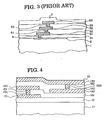
- Fig. 3 shows a conceptional view of a multilayer interconnection.
- an insulating film 31 is formed on a silicon substrate 1.
- a contact hole 4 is formed to make a connection to an element formation region 2.
- a contact plug 4 is formed to bury the contact hole 4 , whereby the connection of the element formation region 2 to a first wiring layer 51 is achieved.
- connection of the first wiring layer 51 to a second wiring layer 52 is made through a via plug 61 buried in a via hole 61 opened in the insulating film 32.
- the connection of the second wiring layer 52 to a third wiring layer 53 is made via a via plug 62 buried in a via hole 62 again opened in an insulating film 33.
- a thickness of the interlayer insulating film In order to prevent such wiring delay and cross talk, an increase in a distance between upper and lower wirings holding the interlayer insulating film is required, that is, a thickness of the interlayer insulating film must be set large. On the other hand, when the thickness of the interlayer insulating film is set large, the deep contact hole and via hole must be formed deeply. The formation of the deep contact hole and via hole makes a dry etching technique to form these holes more difficult. From this viewpoint, it is necessary to make the thickness of the interlayer insulating film thin as possible.
- a diameter of a contact hole must be less than 1/4 ⁇ m.
- the thickness of the interlayer insulating film must necessarily be less than about 1 ⁇ m.
- the increase in the wiring capacitance being related to the thickness of the interlayer insulating film as to the upper and lower wirings or related to the integration degree of the semiconductor integrated circuit including the wirings formed on the same surface level, it is-necessary to approach the wiring delay and cross talk with means like a distributed constant circuit.
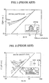
- Fig. 1 shows a capacitance per unit wiring length between a silicon substrate wiring and a wiring layer insulated by an oxide silicon film of a thickness H (specific dielectric constant: 3.9 ), disclosed by L. M. Dang et al., IEEE, Electron Device Letters, No. EDL-Vol. 2, p 196, 1981.
- an insulating film disposed between a silicon substrate and a lowermost wiring as shown in Fig. 1 is never called an interlayer insulating film.
- the problems of the wiring delay and cross talk are common to this insulating film, and, in the description of the specification for this application of the present invention, the insulating film which is formed directly on the silicon substrate to insulating electrically the wirngs shall be also called an interlayer insulating film.
- an operation speed of the elements constituting the semiconductor integrated circuit can be increased by micronizing the elements, when the wirings connecting the elements are micronized, an operation speed of the whole of the semiconductor integrated circuit will never increase because of the increase in the floating capacitance as well as an increase in a wiring resistance.
- Figs. 1 and 2 are given by analyzing the floating capacitance between the silicon substrate and the wiring disposed interposing the insulating film. They are not result concerning the floating capacitance between the wirings. However, the qualitatively equal results can be obtained concerning the floating capacitance between the wiring layers. Therefore, in the description in the specification of this application, the films including an insulating film which is inserted between the silicon substrate and the lowermost wiring layer to electrically insulate them shall be called an interlayer insulating film.
- Heisei 08-236517 (No. Prior Art No. 5). These amorphous carbon fluoride films are formed in such manner that first hydrocarbon type gas and fluorine type gas are changed to plasma gas or CxFy gas is changed to plasma gas, and radical molecules or ions of generated carbon and fluorine react on the silicon substrate to form the amorphous carbon fluoride film.
- Some amorphous carbon fluoride films contains nitrogen atoms or silicon atoms in order to enhance heat resistance property and etching resistance property.
- the foregoing amorphous carbon fluoride film has a low specific dielectric constant ⁇ r, it is expected much as an interlayer insulating film in the multilayer wiring structure.
- the amorphous carbon fluoride film involves technical problems on the formations of a contact hole to connect the wiring to a semiconductor diffusion layer and a via hole to connect between the wirngs. Consequently, putting to practical use of the amorphous carbon fluoride film is obstructed.
- An ordinary resist formed by combining phenol resin and photosensitive material or by combining photosensitive material and resin such as cyclorubber is coated on the amorphous carbon fluoride film to a thickness of 1 to 1.5 ⁇ m, and a hole of a diameter 0.2 ⁇ m is perforated in the amorphous carbon fluoride film, on the supposition of processes for fabricating large scale semiconductor integrated circuit more than 64 megabits DRAM (Dynamic random access memory).
- the foregoing ordinary resist film is coated on the amorphous carbon fluoride film. Thereafter, the resist film is subjected to exposure and developing sequentially, thereby forming a selection mask for selective etching. Subsequently, a hole is formed in the amorphous carbon fluoride film using this resist film as a mask by means of an ion milling method.
- This ion milling method for opening the hole was employed because the amorphous carbon fluoride film exhibits a strong resistance to acid and alkali so that it can not be etched.
- the resist film as the mask itself is etched at the stage of perforation of the hole in the amorphous carbon fluoride film. For this reason, when the resist film of a thickness more than 1 ⁇ m was formed, the opening could be hardly formed for the amorphous carbon fluoride film of a thickness less than 0.4 ⁇ m.
- the perforation of the opening for the amorphous carbon fluoride film of the thickness more than 0.4 ⁇ m was extremely difficult.
- the resist film must be removed after the perforation of the opening by means of the ion milling method. It was found that a reduction in the thickness of the amorphous carbon fluoride film occurs by a wet processing using a resist removing liquid heated to about 100 °C.
- the resist removing was tried by means of ashing processing in oxygen plasma.
- working for the amorphous carbon fluoride film by ordinary photolithography techniques is extremely difficult.
- the object of the present invention is to provide a technology which is capable of solving the foregoing problems and selectively forming contact holes and via holes, in a manufacturing method of a semiconductor device which employs an amorphous carbon fluoride film as an interlayer insulating film having a low specific dielectric constant ⁇ r, the amorphous carbon fluoride film being effective on solving problems of wiring delay and cross talk.
- Another object of the present invention is to provide a semiconductor device which is capable of greatly enhancing heat resistance required for an interlayer insulating film, adhesion of the interlayer insulating film to wiring, low resistivity of a conductive plug formed in a contact hole and a via hole, and reliability of the conductive plug, and a manufacturing method of the same.
- the manufacturing method of the present invention achieves selective formations of the contact hole and the via hole in the interlayer insulating film by etching the amorphous carbon fluoride film containing carbon and fluorine as the main components using a silicone type resist as a selective etching mask.
- the formations of the contact hole and the via hole can be conducted more easily when the etching is performed using oxygen plasma and using the foregoing silicone type resin as the mask.
- the silicone type resist After selectively etching the amorphous carbon fluoride film using the silicone type resist as the mask, the silicone type resist can be easily removed by adopting a method to perform a dry etching in liquid containing hydrofluoric acid which does not etch the amorphous carbon fluoride film or in compound gas containing fluorine.
- a method to perform a dry etching in liquid containing hydrofluoric acid which does not etch the amorphous carbon fluoride film or in compound gas containing fluorine Thus, use of resist remover of complex chemical composition is not necessary. Therefore, clean resist removing process can be realized.
- the amorphous carbon fluoride film having an uneven surface owing to wirings buried therein can be flattened with a good reproducibility.
- the foregoing oxide film, nitride film or oxynitride film serves to increase the adhesion.
- the wirings are electrically insulated from each other by an insulating layer which contains an amorphous carbon fluoride film composed of carbon and fluorine as main components, and the wirings are electrically connected to each other by a conductive material buried in a hole penetrating through the insulating film, whereby a semiconductor device with a small floating capacitance between the wirings can be manufactured, which has a little wiring delay and cross talk.
- the foregoing insulating film includes the amorphous carbon fluoride film containing carbon and fluorine as main components and, at the same time, if the insulating film includes a silicon oxide film, silicon nitride film or silicon oxynitride film, which is formed on at least one major surface of the amorphous carbon fluoride film, the adhesion of the insulating film to a layer formed of such as a metallic material can be enhanced, which is disposed interposing at least the silicon oxide film, silicon nitride film, or silicon oxynitride film which is a composite film of them.
- the selective film A we call these films as "the selective film A."
- the selective film A is formed at an at least interface between a side wall and the amorphous carbon fluoride film exposed to the side wall of hole penetrating the insulating film, a degree of freedom in formation conditions for a conductive plug, such as heating temperature, buried in this hole is greatly increased.
- a semiconductor device having a conductive plug of a small specific resistance will be given.
- the stoichiometric ratio at the at least interface portion is set excessive in silicon, where the selective film A or silicon oxynitride film, which is formed on the side wall of the hole, contacts with the amorphous carbon fluoride film, a semiconductor device having a high adhesion of the amorphous carbon fluoride with the conductive plug will be given, which is excellent in reliability.
- the insulating film includes the amorphous carbon fluoride film containing carbon and fluorine as main components and one of the selective film A formed on at least an upper surface of the amorphous carbon fluoride film, a cross section area of the hole of the amorphous carbon fluoride film is larger than that of the selective film A of the insulating film, and the side wall formed of the selective film A is formed at the at least interface portion between the side wall of the hole penetrating through the insulating film and the amorphous carbon fluoride film exposed to the side wall, the conductive plug of a low resistivity with stability, which conforms with a resist pattern, can be formed without reducing the cross section area due to the side wall.
- Prevention of the reduction in the cross section area due to the formation of the side wall can also achieved by making smaller the thickness of the selective film A, formed on the side wall of the hole, than that of the selective film A included in the insulating film, formed on the amorphous carbon fluoride film.
- the amorphous carbon fluoride film is employed as an interlayer insulating film, and the opening portion is formed in the amorphous carbon fluoride film and the conductive material is buried in the opening portion, thereby being provided with the structure with high reproducibility and reliability.
- the technology as to a selective etching method for this opening portion is provided.
- a photosensitive silicone resin type resist is used as a selective etching mask, and (2) an etching of an amorphous carbon fluoride film is performed by exposing the amorphous carbon fluoride film to oxygen plasma. Thereafter, (3) the photosensitive silicone resin type resist as the selective etching mask is removed by a fluoric acid etching liquid or in gas containing fluorine, thereby manufacturing the semiconductor device.
- the side wall formed of the selective film A is previously formed on the side surface of the opening portion, whereby the structure with high reproducibility and reliability can be obtained.
- the amorphous carbon fluoride film can be etched effectively by exposing it to oxygen plasma
- the ordinary resist when used as a mask in the selective etching, the resist is exposed to the oxygen plasma so that the resist itself is attacked by the oxygen plasma.
- the ordinary resist which is an organic substance composed of carbon atoms as main components is exposed to the oxygen plasma, and the carbon atoms are lost in the form of gas such as carbon monoxide and carbon dioxide. Specifically, this is because exposing the resist to the oxygen plasma is a removal process itself by the well known ashing treatment for the resist.
- the photosensitive silicone resin type resist is used like the present invention, etching using the oxygen plasma, which is capable of effectively etching the amorphous carbon fluoride film, will be possible.
- the base range of the photosensitive silicone resin type resist is a compound formed of silicon atoms as main components, this vapor pressure is low so that the resist is never lost, though couplings of silicon and oxygen increase in exposing the resist to the oxygen plasma.
- the selective etching of the amorphous carbon fluoride film could be performed using the conventional ordinary resist as a mask by means of the technique such as the ion milling, it is impossible to employ the ashing treatment to oxygen plasma in a resist removing step after etching while exposing the amorphous carbon fluoride film plasma. Therefore, although a treatment in strong alkali resist removing liquid is necessary, the amorphous carbon fluoride film itself is attacked by the resist removing liquid.
- the amorphous carbon fluoride film also dissolves in aromatic hydrocarbon such as xylene and ketone solvent such as acetone, and hydrofluoric acid liquid such as dilute hydrofluoric acid can be used for more complete resist removal.
- aromatic hydrocarbon such as xylene and ketone solvent such as acetone
- hydrofluoric acid liquid such as dilute hydrofluoric acid can be used for more complete resist removal.
- the amorphous carbon fluoride film itself is not attacked by these liquids so that reproducibility of the processes can be significantly enhanced.
- the side wall formed of a silicon nitride film and the like is provided on an inner wall of the opening portion.
- a multilayer interconnection having a three layer structure as shown in Fig. 4 will be described. It is natural that any multilayer structure may be realized with repeated usage of the following techniques. Manufacturing processes of Fig. 4 are shown in Fig. 5.
- a lowermost wiring layer 131 is provided on a silicon wafer 11 interposing an insulating film 12.
- an element region such as a diffusion layer.
- a second wiring layer 132 is provided on the lowermost wiring layer 131 interposing an interlayer insulating film 141.
- a third wiring layer 133 is provided interposing the interlayer insulating film 142.
- the uppermost and lowermost wiring layers are electrically connected by via plugs 1511 and 1521 buried in via holes 151 and 152 formed in the interlayer insulating film 141.
- Fig. 4 shows a multilayer interconnection having a three layer structure. It is natural that any multilayer interconnection structure may be obtained by stacking wiring layers on another interposing an interlayer insulating film. An insulating film 16 for passivation is usually deposited on the uppermost wiring layer.
- an amorphous carbon fluoride film of a low dielectric coefficient, which contains carbon and fluorine as main components, is used as the interlayer insulating films 141 and 142.
- This multilayer interconnection structure of this semiconductor device is formed on an insulating film 12 such as phosphorus glass (PSG), which is previously formed on a silicon wafer 11 by an ordinary chemical vapor phase growth (CVD) technique.
- a diffusion layer and the like (not shown), which are element isolation regions, are formed before the formation of the multilayer interconnection structure.
- connection hole to a semiconductor element on the silicon wafer 11 (contact hole) (not shown) is formed by an ordinary method. It should be noted that an amorphous carbon fluoride film is not used as an insulating film formed directly on the silicon substrate 11 and an ordinary PSG film 12 is used as described above.
- a layer for the first wiring layer 131 serving as the lowermost layer is formed on the entire surface of the insulating film 12 by a sputtering method for tungsten. Subsequently, an Al layer having a total thickness of 150 nm is formed by a CVD method. Thereafter, a selective etching mask is formed using an usual lithography technique. The layer for the first wiring layer 131 is subjected to an ordinary dry etching, whereby the first lower wiring layer 131 is obtained.
- the minimum line width of the lower wiring layer 131 shall be 0.25 ⁇ m, and the minimum wiring interval shall be 0.35 ⁇ m.
- the formation of the amorphous carbon fluoride film 141 as in interlayer insulating film will be described by the method disclosed in the specifications of Japanese Patent laid Open No. Heisei 8-838428, No. Heisei 8-222557, and No. Heisei 8-236517.
- the film formation method of the amorphous carbon fluoride film is similar to that disclosed in the specification of Japanese Patent Laid Open No. Heisei 8-236517, the film formation method will be described.
- the film formation of the amorphous carbon fluoride film is conducted using a plasma apparatus.
- the plasma apparatus is constructed such that a pair of upper and lower electrodes are disposed in a vacuum chamber, a silicon wafer is placed on the lower electrode, and high frequency of 400 kHz or 13.56 MHz is applied to the lower electrode independently from a plasma source.
- Plasma is generated by applying high frequency to an electrode disposed separately from the lower electrode.
- the silicon wafer with the insulating film formed thereon, on which the lower wiring layer 131 is formed as shown in Fig. 5(a), is introduced into a preparatory chamber, the preparatory chamber being formed by isolating with a gate bulb at a pre-stage of a plasma generating chamber. Air in the preparatory chamber is evacuated therefrom so that the degree of vacuum is made 10 7 Torr. Thereafter, the gate bulb is opened and the silicon wafer is introduced into the plasma generation chamber kept at a high vacuum less than 10 8 Torr, and the silicon wafer is placed on the lower electrode.
- temperature of the substrate on deposition of the amorphous carbon fluoride film should be less than 200 °C. This is because a deposition speed of the film is substantially zero when the temperature of the substrate exceeds 200 °C. Dependency on temperature of the deposition speed is not made yet clear. It is considered that an adhesion coefficient of reaction seeds to the substrate for formation of the amorphous carbon fluoride film may reduce rapidly with an increase in the temperature.
- the reason why nitrogen is added to raw material gas in this embodiment, is to increase the heat resistance of the amorphous carbon fluoride film as described in the specification of Japanese Patent Application No. Heisei 7-35023. It is natural that the technology of the present invention may be effectively applicable to the amorphous carbon fluoride film to which no nitrogen gas is added.
- At least one gas selected from fluorine gases such as CF4, C2F6, C3F8 and CHF3 can be employed, as a matter of course.
- gas obtained by mixing hydrogen gas H2 with them or gas obtained by mixing at least one gas selected from hydrocarbon gas CH 4 , C 2 H 6 , C 2 H 4 , C 2 H 2 , and C 3 H 8 with them may be employed.
- Fluorine gas such as SF6 and NF3 and the above mentioned hydrocarbon gas may be employed.
- nitrogen gas N 2 may be added for forming the amorphous carbon fluoride film, and at least one selected from NO, NO 2 , NH 3 , and NF 3 also may be added for forming the amorphous carbon fluoride film.
- an apparatus having an ordinary plasma chamber of parallel plate type may be used. It is a matter of course that in order to increase throughput, various kinds of plasma sources such as an ECR (Electron Cyclotron Resonance) plasma source advantageous for high density plasma generation and a silicon wave plasma source may be employed.
- ECR Electro Cyclotron Resonance
- the amorphous carbon fluoride film containing scarcely any hydrogen will be possible, especially depending on a high density plasma source represented by the silicon wave plasma source, in which a substrate and a plasma generation electrode are individually arranged.
- the high density plasma source is advantageous in burying an interlayer insulating film between wiring layers of a large aspect ratio with a good flatness. Little content of hydrogen in the amorphous carbon fluoride film is very important in a sense of heat resistance of the interlayer insulating film.
- composition of the amorphous carbon fluoride film it is desirable that the content of carbon should be less than 70 % in order to obtain a low dielectric constant less than 3.
- the composition is sometimes changed in a film thickness direction in such manner that the content of fluorine at the interface is made extremely small and the carbon content is made more than 70 %.
- the technology of the present invention can be applicable to such film.
- a silicon oxide (SiO 2 ) film, a silicon nitride (SiNx) film, or an oxynitiride (SiON) film which is a complex film formed of the silicon oxide film and the silicon nitride film is formed as a lower thin film of about several nm under the amorphous carbon fluoride film, an increase in adhesion can be brought about.
- the silicon oxide film and the silicon nitride film the excessive content of silicon in them compared to their stoichiometric ratio increases more adhesion.
- an addition of hydrogen to the amorphous carbon fluoride film of several nm thick serving as an interface between the silicon oxide film and the silicon nitride film is effective to increase the adhesion.
- addition of hydrogen increases the adhesion.
- a photosensitive silicone type resist is used as a photoresist.
- the photosensitive silicone type resist is coated by a spinner (not shown).
- the coated resist is exposed so that selective etching pattern (not shown) is formed to open the via hole 151.
- selective etching for the amorphous carbon fluoride film 141 is conducted.
- the selective etching was conducted according to the oxygen plasma method instead of the ion milling method.
- Well known conditions of ashing of the ordinary resist can be principally employed as those of dry etching in the oxygen plasma method, whereby the selective etching is possible over wide range of conditions.
- the via hole 151 is formed under the conditions that a negative bias of several tens to several hundred volts is applied to one electrode on which the substrate is placed, in similar manner to the formation of the amorphous carbon fluoride film.
- the side etching can be controlled in the formation of the via hole 151.
- Figure 6 shows a etching speed in a film thickness direction of amorphous carbon containing fluorine for a negative bias applied to one electrode on which the substrate is placed.
- the negative bias is zero
- the side etching of at least about 70 % of the etching speed in the film thickness direction is observed at an upper portion of the opening.
- the negative bias of -60 V the etching speed in the film thickness direction becomes three times. The side etching quantity reduces adversely so that the side etching is hardly observed.
- the ion milling method has been used as the last resort from the following reason.
- oxygen plasma etching if ordinary phenol resin is used as a base resin, the photoresist itself is ashed by exposing the photoresit to the oxygen plasma so that the photoresist is etched when the amorphous carbon fluoride film is etched.
- the photosensitive silicone resin type resist only the amorphous carbon fluoride film 141 will be selectively etched without apprehending that the resist is lost.
- the base resin of the resist is ordinary organic substance formed of carbon and hydrogen as main components, which includes no phenol resin type silicon, carbon contained in the resist changes to carbon dioxide gas or carbon monoxide gas with exposure to the oxygen plasma, whereby the resist material itself is lost.
- the base resin of the photosensitive silicone resin type resist is formed of polyrudder siloxane or end hydroxy polyrudder siloxane, or both of them, disclosed in Japanese Examined Patent Publication No. Shou 40-15989 and United States Patent No. 3017386.
- these base resin materials are compounds that include Si atoms, although bonds of Si and oxygen increase in the base resin material on exposing to the oxygen plasma, the base resin materials are never lost. Therefore, these base resin materials are preferable.
- Another advantage of the usage of the photosensitive silicone resin type resist as the resist is that hydrofluoric acid type liquid can be employed for removing the resist.
- the amorphous carbon fluoride film 141 itself can not resist in the foregoing so called ashing treatment of the resist and can not used.
- the resist must be removed by strong alkali resist removing liquid which is heated to about 100 °C.
- the amorphous carbon fluoride film 141 solves in the strong alkali resist removing liquid heated to about 100 °C.
- the photosensitive silicone resin type resist also solves in solvent of aromatic hydrocarbon such as xylene and ketone type solvent, and the photosensitive silicone resin type resist is removed easily by hydrofluoric acid liquid such as dilute hydrofluoric acid. These liquid do not solve the amorphous carbon fluoride film 141 itself, whereby reproducibility of the process increases.
- the step advances to a process to bury the conductive plug 1511 in the via hole 151 by means of tungsten CVD.
- both films are formed in a thickness of at least several nm by sputtering. Thereafter, a tungsten film to completely fill the via hole 151 is formed by means of CVD method using WF6 gas as a raw material.
- the tungsten film deposited except in the via hole 151 is removed by dry etching, whereby the surface of the interlayer insulating film is exposed. By this process, tungsten is buried only in the via hole 151. Thus, the conductive plug 1511 is formed.
- Second wiring layer formation processes will be described along with Figs. 5(c) and 5(d).
- a titanium film and a titanium nitride film are stacked for forming the second wiring layer 132.
- the films are subjected to patterning in the same manner as the case of the first wiring layer, whereby the second wiring layer 132 is formed.
- the amorphous carbon fluoride film 142 is formed again, and a vial hole 152 is opened. Further, by coating of tungsten and dry etching, the conductive plug 1521 is buried.
- a side wall such as a silicon nitride film is previously formed on the side surface of the via hole or the contact hole.
- a multilayer interconnection structure having a cross section of Fig. 7 will be described as an example of the second embodiment of the present invention.
- the features of the second embodiment are that the side wall is formed on a side surface of the vial hole or the contact hole, and the amorphous carbon fluoride film 231 is employed also as the insulating film 231 disposed between the lowermost wiring 271 and the diffusion layer 22 formed in the silicon wafer 21.
- the insulating film 231 is first formed on the surface of the silicon wafer 21, in which the diffusion layer 22 is formed.
- a thin silicon oxide film 2311 of 5 nm thick is first formed on the surface of the silicon wafer 21 by oxidation method or CVD method, and, subsequently, an amorphous carbon fluoride film 2312 of 400 nm thick is formed by the foregoing method. Finally, a thin silicon oxide film 2313 of 5 nm thick is formed.
- the formations of the silicon oxide films 2311 and 2313 on and under the amorphous carbon fluoride film 2312 increases the adhesion of the amorphous carbon fluoride film 2312.
- steps for opening the contact hole 241 to connect the diffusion layer 22 with the lowermost wiring 271 begin.
- the foregoing silicone type resist is coated, exposed, and developed (resist step is not shown), thereby forming a resist mask for etching the contact hole 241.
- the silicon oxide film 2313 is etched using hydrofluoric acid type etching liquid.
- the amorphous carbon fluoride film 2312 is etched by the foregoing oxygen plasma, and, then, the silicon oxide film 2311 is etched by the hydrofluoric acid etching liquid.
- the contact hole 241 is opened (Fig. 8(b)).
- the silicone type resist is etched a little. However, the total thickness of all silicon oxide films is as thin as 10 nm, an etching quantity of the silicone type resist is negligible.
- Insulating performance of the amorphous carbon fluoride film is inferior to that silicon oxide film so that the thickness of the silicon oxide films 2311 and 2313 must be sometimes large.
- a two layer structure resist composed of the silicone type resist and ordinary novolak type resist may be used.
- the novolak type resist When the upper silicon oxide film 2313 is thick, an ordinary resist in which the novolak type resist is disposed on the silicone type resist may be used. When the lower silicon oxide film 2311 is thick, the novolak type resist should be disposed under the silicone type resist.
- both films having specific dielectric constants ⁇ 1 and ⁇ 2, respectively, electrodes are formed on the front and back surfaces of the stacked film.
- an equivalent dielectric constant ⁇ r 2.73.
- a dielectric constant of the interlayer insulating film is made sufficiently low.
- the silicon nitride film 25 of 300 nm thick is formed by CVD method.
- the silicon nitride film side wall 251 is formed on the inner wall of the contact hole 241 as shown in Fig. 8(c).
- the conductive film 26 such as tungsten is formed by CVD method in the same manner as the first embodiment.
- the conductive film deposited at the portion other than the contact hole 241 is removed by dry etching, whereby the surface of the interlayer insulating film 231 is exposed. After these processes, as shown in Fig. 8(e), tungsten is buried only in the contact hole 241 so that the conductive plug 261 is formed.
- the silicon nitride film is used as the side wall 251.
- a silicon nitride film or an oxynitride film may also be used.
- composition of at least a film adjacent to the amorphous carbon fluoride film 2312, which is exposed to the side wall of the selective film A is made excessive in silicon compared to each stoichiometric ratio, adhesion of these films to the side wall more increases.
- Fig. 8(g) shows a stage that side etching of the amorphous carbon fluoride film 2312 is conducted until the side of the film 2312 is etched by 200 nm after the film 2312 is slightly over-etched by the plasma etching and the silicon nitride film 25 is formed. In this case, a flaw 23131 occurs in the oxide film 2313.
- the side wall 251 is formed by an anisotropic etching.
- the silicon nitride film 25 sometimes remains at the bottom 2411 of the contact hole 241.
- etching to form the side wall 251 can be continued theoretically sufficiently until the eave 23131 at least disappears. However, it suffices that the etching is stopped before the eave 23131 disappears. At the same time, stopping the etching before the eave disappears is preferable for completely sealing the amorphous carbon fluoride film 2312.
- the oxide film 2313 is formed so as to have a lager film thickness than that of the side wall nitride film 25, this process will be extremely stable, and the low resistivity conductive plug may be formed with reproducibility certainly covering the amorphous carbon fluoride film 2312. Specifically, the nitride film 25 at the bottom 2411 of the contact hole 241 can be securely removed and stable low resistivity contact characteristics can be obtained.
- a heating temperature of the silicon wafer must be 400 °C or less when tungsten is deposited for the formation of the conductive film using a technology such as a CVD method.
- the side wall 251 is provided as this embodiment of the present invention, it is possible to form the conductive film 26 at a temperature of 400 °C or more.
- the formation of the tungsten film at a temperature of 400 °C or less produces the problems of a reduction in a film formation speed and an increase in resistivity of the formed film. Therefore, reliability of the processes is increased by forming the side wall 251 with the structure having the amorphous carbon fluoride film.
- the first wiring layer 271 is formed in the similar manner to the first embodiment.
- the second insulating film 232 is formed in the similar manner to the case of the lower insulating film 231, which is constituted by the amorphous carbon fluoride film 2322 provided between the upper and lower silicon oxide films 2321 and 2323.
- the upper silicon oxide film 2323 constituting the insulating film 232 functions effectively to detect the final point of the CMP. Specifically, at the time when the silicon oxide film 2323 is left only in the recessed portion of the amorphous carbon fluoride film 2322 in Fig. 8(e), the polishing is finished as shown in Fig. 8(f). According to this, since the silicon oxide film 2323 is harder than the amorphous carbon fluoride film 2322 so that a polishing speed drops. As a result, detection of the final point of CMP is easy.
- the via hole 242 is formed conforming to the method of the formation of the contact hole 241.
- the treatment is unnecessary with hydrofluoric acid type etching liquid, prior to etching of the amorphous carbon fluoride film 2322 with oxygen plasma described in the first embodiment.
- a titanium film and a titanium nitride film must be previously deposited.
- the silicon oxide film was used for the insulating film 2323. It is needless to say that a silicon nitride film or an oxynitride film may be used for the insulating film 2323.
- the usage of the technology for formations of the titanium layer or titanium nitride layer under the conductive layer has been always effective, in order to increase adhesion of the conductive material to the insulating film.
- the selective etching of the interlayer insulating film including the amorphous carbon fluoride film using phenol resin type resist or cyclorubber type resist has been difficult.
- the amorphous carbon fluoride film including carbon and fluorine as main components is subjected to the selective etching using silicone type resist as a selective etching mask, whereby workings for forming the contact hole and the via hole in the interlayer insulating film will be conducted easily by means of the oxygen plasma etching.
- the wiring layers are electrically coupled by the conductive material buried in the hole penetrating through the insulating film, each wiring being disposed with electrical isolation from others by the insulating film which includes the amorphous carbon fluoride film containing carbon and fluorine as main components. Therefore, the floating capacitance between the wiring layers will be small, and even in the semiconductor integrated circuit device in which the width of the wiring layer is about 2 ⁇ m, the semiconductor device without the problems of the wiring delay and the cross talk will be achieved. It may be said in passing that the wiring delay time in the present invention can be shortened to approximately half of the case where the silicon oxide film is used as the insulating film, provided that the wiring layers of the same shape are employed in both cases.
- the selective film A is formed at least on one major surface of the amorphous carbon fluoride film and the whole of the amorphous carbon fluoride film and the film formed thereon works as the interlayer insulating film
- the adhesion of the material layer such as the metallic material with the interlayer insulating film can be improved, the material layer being disposed on the amorphous carbon fluoride film interposing the selective film A.
- the stability of the processes can be increased, making it possible to finish the semiconductor device with a high reliability.
- the adhesion is more increased, whereby the stability of the processes and the reliability of the semiconductor device can be more increased.
- the stoichiometric ratio at the interface between the selective film A and the at least amorphous carbon fluoride film is excessive in silicon, the same effects can be obtained.
- the silicone type resist After the amorphous carbon fluoride film is selectively etched using the silicone type resist as a mask, if the method is adopted in which the silicone type resist is subjected to a dry etching by liquid containing fluorine which does not attack the amorphous carbon fluoride film or by compound gas containing fluorine, the silicone type resist can be easily removed. Therefore, it is unnecessary to use a strong alkali resist remover having a complex composition so that a clean resist removing process can be realized.
- the side wall composed of the selective film A which are arranged at the cross section of the amorphous carbon fluoride film exposed to the side surface of the hole bored in the insulating film including at least the amorphous carbon fluoride film, is formed, the degree of freedom of the forming conditions for the conductive plug to be buried in this hole is significantly increased, and the semiconductor device with a low resistivity conductive plug can be obtained.
- the composition of the film adjacent to the amorphous carbon fluoride film contains excessive silicon compared with each stoichiometric ratio, the amorphous carbon fluoride film being exposed to the at least side surface of the selective film A, whereby the adhesion of the amorphous carbon fluoride film with the side wall can be increased, and problems of dusts generated due to peeling-off of the side wall, which occurs occasionally at the periphery of the wafer, is solved.
- the insulating film comprises the amorphous carbon fluoride film containing carbon and fluorine as main components, selective film A, formed at least on the upper surface of the amorphous carbon fluoride film; if the opening cross section area of the foregoing hole in the amorphous carbon fluoride film is set larger than that of the hole to make electrical connections between the wiring layers, bored in one of the selective A of the insulating layer; and if the selective film A is provided at the interface of the amorphous carbon fluoride film exposed to the at least side surface of the hole bored in the insulating film, the stable and low resistivity conductive plug conforming to the resist pattern can be formed without reducing the opening cross section area by the side wall.
- the selective film A to increase the adhesion is formed on the upper surface of the amorphous carbon fluoride film, and the wiring layer is buried therein, so that the unevenness occurs.
- the insulating film can be flattened with a good reproducibility by polishing using the foregoing selective film A as a final point detection means of polishing, which exist in a concaved portion.
- the semiconductor device having the multilayer interconnection structure can be realized, in which many properties such as a stability and reproducibility of multilayer insulation processes, the degree of freedom, the adhesion between layers, and performance of the conductive plug, can be increased.
Landscapes
- Internal Circuitry In Semiconductor Integrated Circuit Devices (AREA)
- Drying Of Semiconductors (AREA)
- Formation Of Insulating Films (AREA)
- Local Oxidation Of Silicon (AREA)
Applications Claiming Priority (2)
| Application Number | Priority Date | Filing Date | Title |
|---|---|---|---|
| JP8049765A JP2956571B2 (ja) | 1996-03-07 | 1996-03-07 | 半導体装置 |
| JP49765/96 | 1996-03-07 |
Publications (2)
| Publication Number | Publication Date |
|---|---|
| EP0795895A2 true EP0795895A2 (fr) | 1997-09-17 |
| EP0795895A3 EP0795895A3 (fr) | 1998-12-02 |
Family
ID=12840279
Family Applications (1)
| Application Number | Title | Priority Date | Filing Date |
|---|---|---|---|
| EP97103762A Withdrawn EP0795895A3 (fr) | 1996-03-07 | 1997-03-06 | Dispositif semi-conducteur comportant une pluralité de couches de câblage empilées et procédé de fabrication |
Country Status (5)
| Country | Link |
|---|---|
| US (2) | US5866920A (fr) |
| EP (1) | EP0795895A3 (fr) |
| JP (1) | JP2956571B2 (fr) |
| KR (1) | KR100308101B1 (fr) |
| CA (1) | CA2199346C (fr) |
Cited By (6)
| Publication number | Priority date | Publication date | Assignee | Title |
|---|---|---|---|---|
| GB2334818A (en) * | 1996-12-02 | 1999-09-01 | Nec Corp | Interlayer insulator |
| GB2323968B (en) * | 1997-04-02 | 1999-10-27 | Nec Corp | Semiconductor device |
| DE19958906A1 (de) * | 1999-12-07 | 2001-07-05 | Infineon Technologies Ag | Herstellung von integrierten Schaltungen |
| GB2389963A (en) * | 1998-12-04 | 2003-12-24 | Nec Electronics Corp | Semiconductor device and method of manufacture |
| EP1052694A4 (fr) * | 1998-01-10 | 2004-11-24 | Tokyo Electron Ltd | Dispositif a semi-conducteurs presentant une couche isolante constituee d'un film de carbone fluore et procede de production dudit dispositif |
| US7402514B2 (en) * | 2003-01-24 | 2008-07-22 | Texas Instruments Incorporated | Line-to-line reliability enhancement using a dielectric liner for a low dielectric constant interlevel and intralevel (or intermetal and intrametal) dielectric layer |
Families Citing this family (51)
| Publication number | Priority date | Publication date | Assignee | Title |
|---|---|---|---|---|
| US6420095B1 (en) | 1994-03-18 | 2002-07-16 | Fujitsu Limited | Manufacture of semiconductor device using A-C anti-reflection coating |
| US5767012A (en) * | 1996-06-05 | 1998-06-16 | Advanced Micro Devices, Inc. | Method of forming a recessed interconnect structure |
| JP3400918B2 (ja) * | 1996-11-14 | 2003-04-28 | 東京エレクトロン株式会社 | 半導体装置の製造方法 |
| JP3228183B2 (ja) * | 1996-12-02 | 2001-11-12 | 日本電気株式会社 | 絶縁膜ならびにその絶縁膜を有する半導体装置とその製造方法 |
| CN1149646C (zh) | 1997-04-28 | 2004-05-12 | 芝浦机械电子装置股份有限公司 | 真空处理方法及其装置 |
| JPH10321624A (ja) * | 1997-05-20 | 1998-12-04 | Toshiba Corp | 半導体装置の製造方法 |
| US6066893A (en) * | 1997-09-24 | 2000-05-23 | Texas Instruments Incorporated | Contaminant resistant barriers to prevent outgassing |
| US6204168B1 (en) * | 1998-02-02 | 2001-03-20 | Applied Materials, Inc. | Damascene structure fabricated using a layer of silicon-based photoresist material |
| US6277730B1 (en) | 1998-02-17 | 2001-08-21 | Matsushita Electronics Corporation | Method of fabricating interconnects utilizing fluorine doped insulators and barrier layers |
| US7211496B1 (en) * | 1998-04-22 | 2007-05-01 | International Business Machines Corporation | Freestanding multiplayer IC wiring structure |
| US6097092A (en) * | 1998-04-22 | 2000-08-01 | International Business Machines Corporation | Freestanding multilayer IC wiring structure |
| US6448655B1 (en) * | 1998-04-28 | 2002-09-10 | International Business Machines Corporation | Stabilization of fluorine-containing low-k dielectrics in a metal/insulator wiring structure by ultraviolet irradiation |
| JP4355039B2 (ja) | 1998-05-07 | 2009-10-28 | 東京エレクトロン株式会社 | 半導体装置及び半導体装置の製造方法 |
| JP2000133710A (ja) | 1998-10-26 | 2000-05-12 | Tokyo Electron Ltd | 半導体装置及びその製造方法 |
| JP3230667B2 (ja) * | 1998-11-17 | 2001-11-19 | 日本電気株式会社 | 半導体装置の配線構造 |
| US6359328B1 (en) * | 1998-12-31 | 2002-03-19 | Intel Corporation | Methods for making interconnects and diffusion barriers in integrated circuits |
| JP4037561B2 (ja) * | 1999-06-28 | 2008-01-23 | 株式会社東芝 | 半導体装置の製造方法 |
| US20050070945A1 (en) * | 1999-11-02 | 2005-03-31 | Steven Schraga | Single use lancet assembly |
| KR100356476B1 (ko) * | 1999-12-29 | 2002-10-18 | 주식회사 하이닉스반도체 | 반도체 소자의 다마신 공정에서 금속층간 절연막 형성 방법 |
| US6573030B1 (en) * | 2000-02-17 | 2003-06-03 | Applied Materials, Inc. | Method for depositing an amorphous carbon layer |
| JP2002194547A (ja) * | 2000-06-08 | 2002-07-10 | Applied Materials Inc | アモルファスカーボン層の堆積方法 |
| DE10040465A1 (de) * | 2000-08-18 | 2002-03-07 | Infineon Technologies Ag | Prozessführung für eine Metall/Metall-Kontaktherstellung |
| US6395632B1 (en) * | 2000-08-31 | 2002-05-28 | Micron Technology, Inc. | Etch stop in damascene interconnect structure and method of making |
| JP2002118199A (ja) * | 2000-10-10 | 2002-04-19 | Mitsubishi Electric Corp | 半導体装置 |
| US6368924B1 (en) * | 2000-10-31 | 2002-04-09 | Motorola, Inc. | Amorphous carbon layer for improved adhesion of photoresist and method of fabrication |
| US6737222B2 (en) * | 2000-11-21 | 2004-05-18 | Advanced Micro Devices, Inc. | Dual damascene process utilizing a bi-layer imaging layer |
| US7085616B2 (en) | 2001-07-27 | 2006-08-01 | Applied Materials, Inc. | Atomic layer deposition apparatus |
| JP4401070B2 (ja) * | 2002-02-05 | 2010-01-20 | ソニー株式会社 | 半導体装置内蔵多層配線基板及びその製造方法 |
| JP2003257970A (ja) * | 2002-02-27 | 2003-09-12 | Nec Electronics Corp | 半導体装置及びその配線構造 |
| US6541397B1 (en) * | 2002-03-29 | 2003-04-01 | Applied Materials, Inc. | Removable amorphous carbon CMP stop |
| US6780753B2 (en) | 2002-05-31 | 2004-08-24 | Applied Materials Inc. | Airgap for semiconductor devices |
| JP2004134687A (ja) * | 2002-10-15 | 2004-04-30 | Toshiba Corp | 半導体装置及びその製造方法 |
| JP2005123406A (ja) * | 2003-10-16 | 2005-05-12 | Tokyo Electron Ltd | プラズマエッチング方法。 |
| WO2005087974A2 (fr) * | 2004-03-05 | 2005-09-22 | Applied Materials, Inc. | Précurseurs liquides pour le dépôt cvd de films de carbone amorphe |
| US7638440B2 (en) * | 2004-03-12 | 2009-12-29 | Applied Materials, Inc. | Method of depositing an amorphous carbon film for etch hardmask application |
| US20050199585A1 (en) * | 2004-03-12 | 2005-09-15 | Applied Materials, Inc. | Method of depositing an amorphous carbon film for metal etch hardmask application |
| US7079740B2 (en) * | 2004-03-12 | 2006-07-18 | Applied Materials, Inc. | Use of amorphous carbon film as a hardmask in the fabrication of optical waveguides |
| KR100726149B1 (ko) * | 2005-06-29 | 2007-06-13 | 주식회사 하이닉스반도체 | 반도체 소자 제조 방법 |
| JP2007294500A (ja) * | 2006-04-21 | 2007-11-08 | Nec Electronics Corp | 半導体装置およびその製造方法 |
| US20070286954A1 (en) * | 2006-06-13 | 2007-12-13 | Applied Materials, Inc. | Methods for low temperature deposition of an amorphous carbon layer |
| US20080254233A1 (en) * | 2007-04-10 | 2008-10-16 | Kwangduk Douglas Lee | Plasma-induced charge damage control for plasma enhanced chemical vapor deposition processes |
| US8021975B2 (en) * | 2007-07-24 | 2011-09-20 | Tokyo Electron Limited | Plasma processing method for forming a film and an electronic component manufactured by the method |
| JP2009064909A (ja) * | 2007-09-05 | 2009-03-26 | Alps Electric Co Ltd | 多層セラミック配線板およびその製造方法 |
| US20090093128A1 (en) * | 2007-10-08 | 2009-04-09 | Martin Jay Seamons | Methods for high temperature deposition of an amorphous carbon layer |
| JP5170101B2 (ja) * | 2007-11-02 | 2013-03-27 | 富士通セミコンダクター株式会社 | 半導体装置とその製造方法 |
| US20090269923A1 (en) * | 2008-04-25 | 2009-10-29 | Lee Sang M | Adhesion and electromigration improvement between dielectric and conductive layers |
| US9653327B2 (en) | 2011-05-12 | 2017-05-16 | Applied Materials, Inc. | Methods of removing a material layer from a substrate using water vapor treatment |
| JP5733623B2 (ja) * | 2011-06-10 | 2015-06-10 | 国立大学法人九州大学 | 半導体装置の製造方法 |
| WO2013112360A1 (fr) * | 2012-01-27 | 2013-08-01 | University Of Kansas | Couches de diffusion de gaz hydrophobe et leur procédé de fabrication |
| US9865459B2 (en) * | 2015-04-22 | 2018-01-09 | Applied Materials, Inc. | Plasma treatment to improve adhesion between hardmask film and silicon oxide film |
| CN110088882B (zh) * | 2016-12-14 | 2023-05-26 | 玛特森技术公司 | 与快速热活化工艺相结合的使用等离子体的原子层刻蚀工艺 |
Family Cites Families (12)
| Publication number | Priority date | Publication date | Assignee | Title |
|---|---|---|---|---|
| US4493855A (en) * | 1982-12-23 | 1985-01-15 | International Business Machines Corporation | Use of plasma polymerized organosilicon films in fabrication of lift-off masks |
| JPS62136820A (ja) * | 1985-12-11 | 1987-06-19 | Nippon Telegr & Teleph Corp <Ntt> | 極微細パタ−ン形成法 |
| US4822716A (en) * | 1985-12-27 | 1989-04-18 | Kabushiki Kaisha Toshiba | Polysilanes, Polysiloxanes and silicone resist materials containing these compounds |
| JPH07113774B2 (ja) * | 1987-05-29 | 1995-12-06 | 株式会社日立製作所 | パタ−ンの形成方法 |
| JPS6489435A (en) * | 1987-09-30 | 1989-04-03 | Hitachi Ltd | Dissolution removing method of resist |
| KR920018987A (ko) * | 1991-03-23 | 1992-10-22 | 김광호 | 캐패시터의 제조방법 |
| JP3010824B2 (ja) * | 1991-09-17 | 2000-02-21 | 株式会社日立製作所 | 半導体装置及びその製造方法 |
| US5559367A (en) * | 1994-07-12 | 1996-09-24 | International Business Machines Corporation | Diamond-like carbon for use in VLSI and ULSI interconnect systems |
| JP2748879B2 (ja) * | 1995-02-23 | 1998-05-13 | 日本電気株式会社 | フッ素化非晶質炭素膜材料の製造方法 |
| CA2157257C (fr) * | 1994-09-12 | 1999-08-10 | Kazuhiko Endo | Dispositif a semiconducteur a couche de carbone amorphe et sa methode de fabrication |
| JP2748864B2 (ja) * | 1994-09-12 | 1998-05-13 | 日本電気株式会社 | 半導体装置及びその製造方法及び非晶質炭素膜の製造方法及びプラズマcvd装置 |
| JP2751851B2 (ja) * | 1995-02-09 | 1998-05-18 | 日本電気株式会社 | フッ素化非晶質炭素膜の製造方法 |
-
1996
- 1996-03-07 JP JP8049765A patent/JP2956571B2/ja not_active Expired - Lifetime
-
1997
- 1997-03-06 CA CA002199346A patent/CA2199346C/fr not_active Expired - Fee Related
- 1997-03-06 EP EP97103762A patent/EP0795895A3/fr not_active Withdrawn
- 1997-03-07 KR KR1019970008129A patent/KR100308101B1/ko not_active Expired - Fee Related
- 1997-03-07 US US08/813,338 patent/US5866920A/en not_active Expired - Lifetime
-
1999
- 1999-01-14 US US09/231,493 patent/US6180531B1/en not_active Expired - Lifetime
Cited By (9)
| Publication number | Priority date | Publication date | Assignee | Title |
|---|---|---|---|---|
| GB2334818A (en) * | 1996-12-02 | 1999-09-01 | Nec Corp | Interlayer insulator |
| GB2334818B (en) * | 1996-12-02 | 2000-07-19 | Nec Corp | An insulating film, a semiconductor device and methods for their manaufacture |
| GB2323968B (en) * | 1997-04-02 | 1999-10-27 | Nec Corp | Semiconductor device |
| US6104092A (en) * | 1997-04-02 | 2000-08-15 | Nec Corporation | Semiconductor device having amorphous carbon fluoride film of low dielectric constant as interlayer insulation material |
| EP1052694A4 (fr) * | 1998-01-10 | 2004-11-24 | Tokyo Electron Ltd | Dispositif a semi-conducteurs presentant une couche isolante constituee d'un film de carbone fluore et procede de production dudit dispositif |
| EP1947685A3 (fr) * | 1998-01-10 | 2008-08-27 | Tokyo Electron Limited | Dispositif à semi-conducteur ayant un film diélectrique en carbone ajouté à la fluorine et son procédé de fabrication |
| GB2389963A (en) * | 1998-12-04 | 2003-12-24 | Nec Electronics Corp | Semiconductor device and method of manufacture |
| DE19958906A1 (de) * | 1999-12-07 | 2001-07-05 | Infineon Technologies Ag | Herstellung von integrierten Schaltungen |
| US7402514B2 (en) * | 2003-01-24 | 2008-07-22 | Texas Instruments Incorporated | Line-to-line reliability enhancement using a dielectric liner for a low dielectric constant interlevel and intralevel (or intermetal and intrametal) dielectric layer |
Also Published As
| Publication number | Publication date |
|---|---|
| KR100308101B1 (ko) | 2001-11-30 |
| JPH09246242A (ja) | 1997-09-19 |
| JP2956571B2 (ja) | 1999-10-04 |
| CA2199346A1 (fr) | 1997-09-07 |
| CA2199346C (fr) | 2001-06-05 |
| KR970067703A (ko) | 1997-10-13 |
| US5866920A (en) | 1999-02-02 |
| EP0795895A3 (fr) | 1998-12-02 |
| US6180531B1 (en) | 2001-01-30 |
Similar Documents
| Publication | Publication Date | Title |
|---|---|---|
| US5866920A (en) | Semiconductor device and manufacturing method of the same | |
| US6372628B1 (en) | Insulating film comprising amorphous carbon fluoride, a semiconductor device comprising such an insulating film, and a method for manufacturing the semiconductor device | |
| CN1145209C (zh) | 半导体器件的形成方法 | |
| USRE38914E1 (en) | Dual damascene patterned conductor layer formation method without etch stop layer | |
| US5795823A (en) | Self aligned via dual damascene | |
| US6140224A (en) | Method of forming a tungsten plug | |
| US4946550A (en) | Forming electrical connections for electronic devices | |
| US5668052A (en) | Method of manufacturing semiconductor device | |
| EP0523856A2 (fr) | Procédé de formation d'un via pour circuits integrés à interconnexions à multiples niveaux | |
| USRE38363E1 (en) | Method of forming trench isolation having polishing step and method of manufacturing semiconductor device | |
| EP0424485B1 (fr) | Methode d'interconnexion entierement encastree ayant du titane-tungstene et du tungstene a procede cvd selectif | |
| JPH09181181A (ja) | 接点領域上の横方向スペーサの腐食を最小にする処理方法及び半導体装置 | |
| US5591675A (en) | Interconnecting method for semiconductor device | |
| JPH07273063A (ja) | 半導体装置およびその製造方法 | |
| US5663108A (en) | Optimized metal pillar via process | |
| JPH01503021A (ja) | シリコンウエハ内に貫通導体を形成する為の平担化方法 | |
| US7056823B2 (en) | Backend metallization method and device obtained therefrom | |
| US6410424B1 (en) | Process flow to optimize profile of ultra small size photo resist free contact | |
| JP3312604B2 (ja) | 半導体装置の製造方法 | |
| US6881661B2 (en) | Manufacturing method of semiconductor device | |
| JP3074171B1 (ja) | 層間絶縁膜の形成方法、及び半導体装置 | |
| JP3317279B2 (ja) | 半導体装置の製造方法 | |
| KR100328449B1 (ko) | 반도체 소자의 다마신 패턴을 이용한 금속배선 형성방법 | |
| JP3239944B2 (ja) | 半導体装置の製造方法 | |
| JP2001015596A (ja) | 半導体装置の製造方法 |
Legal Events
| Date | Code | Title | Description |
|---|---|---|---|
| PUAI | Public reference made under article 153(3) epc to a published international application that has entered the european phase |
Free format text: ORIGINAL CODE: 0009012 |
|
| AK | Designated contracting states |
Kind code of ref document: A2 Designated state(s): DE FR GB IT NL |
|
| PUAL | Search report despatched |
Free format text: ORIGINAL CODE: 0009013 |
|
| AK | Designated contracting states |
Kind code of ref document: A3 Designated state(s): DE FR GB IT NL |
|
| 17P | Request for examination filed |
Effective date: 19981103 |
|
| 17Q | First examination report despatched |
Effective date: 20040518 |
|
| STAA | Information on the status of an ep patent application or granted ep patent |
Free format text: STATUS: THE APPLICATION HAS BEEN WITHDRAWN |
|
| 18W | Application withdrawn |
Effective date: 20040811 |