EP0817272A2 - Circuit intégré contenant un condensateur - Google Patents
Circuit intégré contenant un condensateur Download PDFInfo
- Publication number
- EP0817272A2 EP0817272A2 EP97110460A EP97110460A EP0817272A2 EP 0817272 A2 EP0817272 A2 EP 0817272A2 EP 97110460 A EP97110460 A EP 97110460A EP 97110460 A EP97110460 A EP 97110460A EP 0817272 A2 EP0817272 A2 EP 0817272A2
- Authority
- EP
- European Patent Office
- Prior art keywords
- integrated circuit
- area
- power supply
- semicustom
- capacitor
- Prior art date
- Legal status (The legal status is an assumption and is not a legal conclusion. Google has not performed a legal analysis and makes no representation as to the accuracy of the status listed.)
- Granted
Links
Images


Classifications
-
- H—ELECTRICITY
- H10—SEMICONDUCTOR DEVICES; ELECTRIC SOLID-STATE DEVICES NOT OTHERWISE PROVIDED FOR
- H10D—INORGANIC ELECTRIC SEMICONDUCTOR DEVICES
- H10D84/00—Integrated devices formed in or on semiconductor substrates that comprise only semiconducting layers, e.g. on Si wafers or on GaAs-on-Si wafers
- H10D84/90—Masterslice integrated circuits
-
- H—ELECTRICITY
- H10—SEMICONDUCTOR DEVICES; ELECTRIC SOLID-STATE DEVICES NOT OTHERWISE PROVIDED FOR
- H10D—INORGANIC ELECTRIC SEMICONDUCTOR DEVICES
- H10D84/00—Integrated devices formed in or on semiconductor substrates that comprise only semiconducting layers, e.g. on Si wafers or on GaAs-on-Si wafers
- H10D84/90—Masterslice integrated circuits
- H10D84/903—Masterslice integrated circuits comprising field effect technology
- H10D84/907—CMOS gate arrays
Definitions
- This invention relates to an improvement applicable to an integrated circuit. More specifically, this invention relates to an improvement developed for enabling a semicustom integrated circuit particularly a semicustom LSI to exclude external noises particularly noises originated from a power supply, from the semicustom integrated circuit.
- An IC or LSI available in the prior art usually has a circuit having a capacitor connected in series with earth, the circuit being arranged between the core domain and the I/O domain of the IC or LSI.
- the function of the circuit is to prevent external noises from flowing into the major circuits of the IC or LSI and to expel them toward outside of the IC or LSI.
- a semicustom IC or LSI has a plurality of unit cells arranged in a regular lattice pattern or in a matrix pattern.
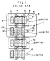
- Fig. 1 illustrates the plan view of the unit cell of a semicustom LSI.
- the numeral 1 shows a unit cell having a P channel transistor 2 and an N channel transistor 11 therein.
- the P channel transistor 2 has an N - doped semiconductor layer 3 whose potential is selected to be identical to the substrate potential.
- the numeral 4 shows an N + active area located in the N - doped semiconductor layer 3.
- the numeral 5 shows a P semiconductor substrate
- the numeral 6 shows an N well produced in the P semiconductor substrate
- the numeral 7 shows gates
- the numeral 8 shows a P - doped semiconductor layer
- the numeral 9 shows a P + active area located in the P - doped semiconductor layer 8
- the numeral 10 shows a VDD line.
- the N channel transistor 11 has a P - doped semiconductor layer 12 whose potential is selected to be identical to the substrate potential.
- the numeral 13 shows a P + active area located in the P - doped semiconductor layer 12, the numeral 14 shows an N - doped semiconductor layer, the numeral 15 shows an N + active area, the numeral 16 shows gates and the numeral 17 shows a VSS line.
- the foregoing capacitor is required to have a relatively large amount of capacity. This resultantly requires a large horizontal area on an IC chip. Since improvement in integration is one of the most important requirements for an IC or LSI, the foregoing structure of an IC or LSI is a big drawback which should be removed by all means.
- an object of this invention is to provide an integrated circuit which does not require an additional horizontal area for arranging a capacitor which is employable to expel higher harmonics contained in a noise originated from a power supply (a power supply noise) toward outside of the integrated circuit.
- An integrated circuit in accordance with the first embodiment of this invention comprising :
- the only structural change applicable to a semicustom IC or LSI available in the prior art for the purpose to produce an integrated circuit in accordance with the first embodiment of this invention is limited to a structural change applicable to a poly crystalline silicon layer which is the bottom layer of a semiconductor IC available in the prior art. It is noted that no change is required for the wirings, and that an area which has not been employed so far is positively employed in the first embodiment of this invention.
- An integrated circuit in accordance with the second embodiment of this invention comprising :
- three independent capacitors are formed by a combination of the middle one of the foregoing three conductive poly crystalline silicon lines, an insulator layer arranged thereunder and a semiconductor layer arranged thereunder, and by combination of the middle one of the foregoing three conductive poly crystalline silicon lines and the end ones of the foregoing three conductive poly crystalline silicon lines, for providing routes for allowing higher harmonics to flow towards outside of the integrated circuit. It is noted that the domain which is remained unemployed in the prior art, is positively employed to enhance the integration.
- An integrated circuit in accordance with the third embodiment of this invention comprising :
- An integrated circuit in accordance with the fourth embodiment of this invention comprising :
- a power supply ring line which surrounds the core domain of an integrated circuit, can be employed to form a capacity.
- An integrated circuit in accordance with the fifth embodiment of this invention comprising :
- An integrated circuit in accordance with the sixth embodiment of this invention comprising :
- the gates of the field effect transistors and the electrode of the capacitor can be made of the same material and made via the same gate insulator layer.
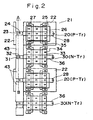
- Fig. 2 is a plan view of a unit cell of a semicustom LSI in accordance with the first embodiment of this invention.
- a semicustom LSI has a plurality of the unit cells illustrated in Fig. 2, the plurality of the unit cells being arranged in a regular lattice pattern or in a matrix pattern.
- One of the plural unit cells is illustrated in Fig. 2.
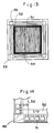
- Fig. 3 is a cross section of Fig. 1, along the A-B line and Fig. 4 is an equivalent circuit diagram of Fig. 3.
- a numeral 20 shows a P channel transistor
- a numeral 21 shows a P substrate
- the numeral 22 shows an N well
- the numeral 24 is an N + active area made in an N - doped semiconductor layer
- the numeral 25 shows a P - doped semiconductor layer
- the numeral 26 shows a P + active area
- the numeral 27 shows gates made of conductive poly crystalline silicon
- the numeral 28 shows a VDD line.
- An N channel transistor 30 has an N - doped semiconductor layer 31, a P + active area produced in the P - doped semiconductor layer, an N - doped semiconductor layer 33, an N + active area produced in the N - doped semiconductor area 33, an N + active area 34, a gate 35 made of conductive poly crystalline silicon and a VSS line 36.
- Poly crystalline silicon layers 43 are produced to cover all the active areas 24 and 32 which are exclusively employed for power supply / GND, to form capacitors each of which consists of the poly crystalline silicon layers 43, the gate insulator 41 and the active area 24 or 32.
- the poly crystalline silicon layers 43 made of conductive poly crystalline silicon is produced in a step for producing the gates 27 or simultaneously with the gates 27. In other words, the poly crystalline silicon layers 43 is produced on an active area 24 or 32, thereby MIS capacitors described above are produced.
- the numeral 42 shows a field insulator layer.
- capacitors are formed by the P + active area 32, a gate insulator layer 41 and the poly crystalline silicon layer 43 and by the N + active area 24, a gate insulator layer 41 and the poly crystalline silicon layer 43. These capacitors are connected in series by the poly crystalline silicon layer 43 produced on the field insulator layer 42, as shown by an equivalent circuit diagram illustrated in Fig. 4.
- the capacitors are formed by combination of the P + active area 32, a gate insulator layer 41 and the poly crystalline silicon layer 43 and of the N + active area 24, a gate insulator layer 41 and the poly crystalline silicon layer 43, no change is required for layer configuration of a semiconductor LSI available in the prior art, to produce a semicustom LSI in accordance with the first embodiment of this invention. Further, since an area which was remained unemployed in the prior art is positively employed in this embodiment of this invention, it is effective to improve the magnitude of integration. In addition, since the dielectric layer 41 of the capacitor is a thin silicon dioxide layer produced by oxidation of silicon in the step for producing the gate insulator layer 41, the capacity of the capacitor is large.
- Fig. 5 is the plan view of a semicustom LSI in accordance with the second embodiment of this invention
- Fig. 6 is an enlarged plan view of the corner (Corner A) of a semicustom LSI in accordance with the second embodiment of this invention
- Fig. 7 is an enlarged plan view of edge B of a semicustom LSI in accordance with the second embodiment of this invention, the edge B being shown in Fig. 6.
- a semicustom LSI in accordance with the second embodiment of this invention consists of a core domain 51, I/O domains 52, corner (Corner A) 53, a power supply ring 54 which surrounds the core domain 51 and three lines 55 each of which is arranged close to one another and which are made of poly crystalline silicon.
- connection pads 56 to be connected with VDD and connection pads 57 to be connected with GND are utilized for producing the three lines 55. It is further noted that the three lines 55 are arranged to make the space therebetween minimum. The three lines 55 surrounds the core domain 51 and the I/O domains 52.
- the three poly crystalline silicon lines arranged close to one another consists of a first poly crystalline silicon line 55A, a second poly crystalline silicon line 55B and a third poly crystalline silicon line 55C.
- the numerals 61 and 63 show respectively a line drawn from the pad 56(GND) and the pad 57(VDD).
- the numerals 62 and 63 show contacts.
- the numeral 65 shows an N well.
- VDD / GND cells are arranged in a wiring step.
- the line 61 drawn from the pad 56(GND) is connected with the second poly crystalline silicon line 55B by the contact 62.
- the line 63 drawn from the pad 57(VDD) is connected with the first poly crystalline silicon line 55A and the third poly crystalline silicon line 55C by the contact 64.
- the second poly crystalline silicon line 55B is arranged on an N + active area
- the first poly crystalline silicon line 55A and the third poly crystalline silicon line 55C are arranged on a P + active area.
- an N well electrically separates the area from the substrate.
- a MIS capacitor is produced by the second poly crystalline silicon line 55B and the lower layers, and fringing capacitors are produced by a combination of the second poly crystalline silicon line 55B and the first poly crystalline silicon line 55A and by a combination of the second poly crystalline silicon line 55B and the third poly crystalline silicon line 55C.
- an integrated circuit in accordance with the second embodiment of this invention is provided with three poly crystalline silicon lines 55A, 55B and 55C which are produced surrounding the core domain and the I/O domains.
- Fig. 8 is a plan view of a semicustom LSI in accordance with the third embodiment of this invention
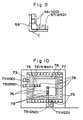
- Fig. 9 is an enlarged plan view of the corner (Corner A) of a semicustom LSI in accordance with the third embodiment of this invention
- Fig. 10 is a more enlarged plan view of the corner (Corner C) of a semicustom LSI in accordance with the third embodiment of this invention. Since the overall structure of and the specific structure of the corner (Corner A) of the semicustom LSI in accordance with the third embodiment of this invention are identical to those of the semicustom LSI in accordance with the second embodiment of this invention, all the members illustrated in Figs. 8 through 10 are allotted numerals identical to those of the corresponding ones of the second embodiment. Thus, eliminated is a detailed description for the general matters of the semicustom LSI in accordance with the third embodiment of this invention.
- a VDD pad 71 which is a fixed pad is connected with a P + active area 78 by contacts 74 at locations where a wiring 73 surrounds an N well 72.
- Upper lines 76 are drawn from a GND pad 75 which is a fixed pad and are connected with a poly crystalline silicon layer 77 by contacts 74 and by second through holes (VIA2) 79.
- the poly crystalline silicon layer 77 is produced on a P + active area 78, and is separated from a substrate by an N well 72.
- an integrated circuit in accordance with the third embodiment of this invention is provided a poly crystalline silicon line produced at the corners of an integrated circuit, the corners which were remained unemployed in the prior art, are positively used to produce capacitors which are employed to exclude external noises from the integrated circuit.
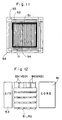
- Fig. 11 is a plan view of a semicustom LSI in accordance with the fourth embodiment of this invention
- Fig. 12 is an enlarged plan view of the edge D (power supply ring line) of a semicustom LSI in accordance with the fourth embodiment of this invention.
- processes employed for the second and third embodiments are employed to produce an active layer 81 under the area of the power supply ring line 54.
- the active layer 81 is covered by a poly crystalline silicon layer 82, to form a capacity thereby.
- the numerals 83 and 84 show respectively VDD lines and GND lines.
- a power supply ring line 54 which surrounds the core domain 51 of an integrated circuit, can be employed to arrange a poly crystalline silicon line 55, to form a capacity.
- a poly crystalline silicon layer can be produced on the I/O domains 52 which are produced on the active layer. This layer configuration is also effective to produce a capacitor.
- Fig. 13 is a plan view of semicustom LSI in accordance with the fifth embodiment of this invention and Fig. 14 is an enlarged plan view of the corner of a semicustom LSI in accordance with the fifth embodiment of this invention.
- poly crystalline silicon layers and active regions 92 are arranged in the area where pads 91 are arranged. In this manner, a capacitor can be produced.
- an integrated circuit in accordance with the fifth embodiment of this invention positively employs the area remained unemployed in the prior art.
Landscapes
- Semiconductor Integrated Circuits (AREA)
- Design And Manufacture Of Integrated Circuits (AREA)
- Metal-Oxide And Bipolar Metal-Oxide Semiconductor Integrated Circuits (AREA)
Applications Claiming Priority (3)
| Application Number | Priority Date | Filing Date | Title |
|---|---|---|---|
| JP165469/96 | 1996-06-26 | ||
| JP16546996 | 1996-06-26 | ||
| JP8165469A JPH1012825A (ja) | 1996-06-26 | 1996-06-26 | 半導体集積回路装置 |
Publications (3)
| Publication Number | Publication Date |
|---|---|
| EP0817272A2 true EP0817272A2 (fr) | 1998-01-07 |
| EP0817272A3 EP0817272A3 (fr) | 1998-05-06 |
| EP0817272B1 EP0817272B1 (fr) | 2005-06-15 |
Family
ID=15813013
Family Applications (1)
| Application Number | Title | Priority Date | Filing Date |
|---|---|---|---|
| EP97110460A Expired - Lifetime EP0817272B1 (fr) | 1996-06-26 | 1997-06-26 | Circuit intégré contenant un condensateur |
Country Status (7)
| Country | Link |
|---|---|
| US (1) | US6121645A (fr) |
| EP (1) | EP0817272B1 (fr) |
| JP (1) | JPH1012825A (fr) |
| KR (1) | KR100371678B1 (fr) |
| CN (1) | CN1163967C (fr) |
| DE (1) | DE69733513T2 (fr) |
| TW (1) | TW360981B (fr) |
Families Citing this family (12)
| Publication number | Priority date | Publication date | Assignee | Title |
|---|---|---|---|---|
| US6617620B1 (en) * | 1999-09-29 | 2003-09-09 | Oki Electric Industry Co., Ltd. | Gate array with border element |
| JP3406270B2 (ja) * | 2000-02-17 | 2003-05-12 | 沖電気工業株式会社 | 半導体装置及びその製造方法 |
| JP4092173B2 (ja) | 2002-10-24 | 2008-05-28 | Necエレクトロニクス株式会社 | 半導体集積回路装置 |
| JP4258205B2 (ja) * | 2002-11-11 | 2009-04-30 | パナソニック株式会社 | 半導体装置 |
| JP2004207271A (ja) | 2002-12-20 | 2004-07-22 | Nec Electronics Corp | Soi基板及び半導体集積回路装置 |
| JP4307919B2 (ja) * | 2003-06-27 | 2009-08-05 | 三洋電機株式会社 | 半導体装置の製造方法 |
| CN1305127C (zh) * | 2003-09-12 | 2007-03-14 | 清华大学 | 用去耦合电容实现集成电路供电网络噪声优化的快速方法 |
| US7728362B2 (en) | 2006-01-20 | 2010-06-01 | International Business Machines Corporation | Creating integrated circuit capacitance from gate array structures |
| JP5230912B2 (ja) | 2006-06-08 | 2013-07-10 | ラピスセミコンダクタ株式会社 | 半導体集積回路装置の製造方法 |
| US8558320B2 (en) * | 2009-12-15 | 2013-10-15 | Qualcomm Incorporated | Systems and methods employing a physically asymmetric semiconductor device having symmetrical electrical behavior |
| US9082886B2 (en) * | 2011-05-12 | 2015-07-14 | Taiwan Semiconductor Manufacturing Company, Ltd. | Adding decoupling function for tap cells |
| JP5868682B2 (ja) * | 2011-12-01 | 2016-02-24 | 株式会社ソシオネクスト | 半導体装置 |
Family Cites Families (21)
| Publication number | Priority date | Publication date | Assignee | Title |
|---|---|---|---|---|
| JPS6068662U (ja) * | 1983-10-17 | 1985-05-15 | 三洋電機株式会社 | 集積化コンデンサ |
| JPS60192359A (ja) * | 1984-03-14 | 1985-09-30 | Nec Corp | 半導体メモリ装置 |
| JPS6341048A (ja) * | 1986-08-06 | 1988-02-22 | Mitsubishi Electric Corp | 標準セル方式大規模集積回路 |
| JPS63120446A (ja) * | 1986-11-08 | 1988-05-24 | Mitsubishi Electric Corp | 半導体集積回路装置における電源,接地配線構造 |
| JPS63143843A (ja) * | 1986-12-08 | 1988-06-16 | Nippon Telegr & Teleph Corp <Ntt> | 半導体集積回路電源配線装置 |
| JPH01278749A (ja) * | 1988-04-30 | 1989-11-09 | Seiko Epson Corp | 半導体装置 |
| US5307309A (en) * | 1988-05-31 | 1994-04-26 | Micron Technology, Inc. | Memory module having on-chip surge capacitors |
| JPH02163960A (ja) * | 1988-12-16 | 1990-06-25 | Toshiba Corp | 半導体装置 |
| JPH0397245A (ja) * | 1989-09-11 | 1991-04-23 | Seiko Epson Corp | ゲートアレイ装置 |
| JP3038731B2 (ja) * | 1989-10-19 | 2000-05-08 | ソニー株式会社 | 半導体装置 |
| JPH04196583A (ja) * | 1990-11-28 | 1992-07-16 | Seiko Epson Corp | 半導体装置 |
| US5343058A (en) * | 1991-11-18 | 1994-08-30 | Vlsi Technology, Inc. | Gate array bases with flexible routing |
| JPH05283611A (ja) * | 1992-03-31 | 1993-10-29 | Nec Corp | 半導体装置 |
| JPH05299578A (ja) * | 1992-04-17 | 1993-11-12 | Rohm Co Ltd | 半導体装置およびその製法 |
| JP2855975B2 (ja) * | 1992-07-06 | 1999-02-10 | 富士通株式会社 | 半導体集積回路 |
| JPH06177267A (ja) * | 1992-12-08 | 1994-06-24 | Mitsubishi Electric Corp | 半導体装置 |
| KR940018967A (ko) * | 1993-01-30 | 1994-08-19 | 오가 노리오 | 반도체장치 및 그 제조방법 |
| US5452245A (en) * | 1993-09-07 | 1995-09-19 | Motorola, Inc. | Memory efficient gate array cell |
| JP2919241B2 (ja) * | 1993-09-13 | 1999-07-12 | 日本電気株式会社 | 電源配線 |
| JP2682397B2 (ja) * | 1993-10-07 | 1997-11-26 | 日本電気株式会社 | セルベース設計半導体集積回路装置 |
| US5608258A (en) * | 1995-03-16 | 1997-03-04 | Zilog, Inc. | MOS precision capacitor with low voltage coefficient |
-
1996
- 1996-06-26 JP JP8165469A patent/JPH1012825A/ja not_active Withdrawn
-
1997
- 1997-06-14 TW TW086108242A patent/TW360981B/zh active
- 1997-06-20 KR KR1019970026272A patent/KR100371678B1/ko not_active Expired - Fee Related
- 1997-06-24 US US08/881,500 patent/US6121645A/en not_active Expired - Fee Related
- 1997-06-26 DE DE69733513T patent/DE69733513T2/de not_active Expired - Fee Related
- 1997-06-26 CN CNB971139008A patent/CN1163967C/zh not_active Expired - Fee Related
- 1997-06-26 EP EP97110460A patent/EP0817272B1/fr not_active Expired - Lifetime
Also Published As
| Publication number | Publication date |
|---|---|
| EP0817272A3 (fr) | 1998-05-06 |
| DE69733513D1 (de) | 2005-07-21 |
| KR980006436A (ko) | 1998-03-30 |
| CN1163967C (zh) | 2004-08-25 |
| DE69733513T2 (de) | 2006-05-11 |
| JPH1012825A (ja) | 1998-01-16 |
| EP0817272B1 (fr) | 2005-06-15 |
| KR100371678B1 (ko) | 2003-05-12 |
| TW360981B (en) | 1999-06-11 |
| CN1173740A (zh) | 1998-02-18 |
| US6121645A (en) | 2000-09-19 |
Similar Documents
| Publication | Publication Date | Title |
|---|---|---|
| US5656834A (en) | IC standard cell designed with embedded capacitors | |
| JPS647508B2 (fr) | ||
| US6121645A (en) | Noise-reducing circuit | |
| US5227649A (en) | Circuit layout and method for VLSI circuits having local interconnects | |
| US20010042238A1 (en) | Semiconductor apparatus including bypass capacitor having structure for making automatic design easy, and semiconductor apparatus layout method | |
| JP3163039B2 (ja) | 静電気保護回路を備えた半導体装置 | |
| US6541840B1 (en) | On-chip capacitor | |
| JP2003243522A (ja) | 抵抗素子を使用した半導体装置 | |
| US7739636B2 (en) | Design structure incorporating semiconductor device structures that shield a bond pad from electrical noise | |
| US5434436A (en) | Master-slice type semiconductor integrated circuit device having multi-power supply voltage | |
| JP2001028423A (ja) | 半導体集積回路装置 | |
| TW522523B (en) | Semiconductor device, method of manufacturing the same and storage media | |
| KR100649067B1 (ko) | Mis 커패시터 및 mis 커패시터 제조 방법 | |
| JPH10107235A (ja) | ゲートアレーlsiの構成方法とこれを用いた回路装置 | |
| GB2243485A (en) | Semiconductor device contact pads | |
| US20040226735A1 (en) | Method and apparatus for integrated noise decoupling | |
| JP2840239B2 (ja) | マスタースライス型半導体装置 | |
| EP0104754A1 (fr) | Dispositif métal-isolant semi-conducteur à région de source liée à une tension de référence | |
| CN101499455B (zh) | 应用于结构式特定用途集成电路的电源架构 | |
| JPS61224348A (ja) | 半導体集積回路装置 | |
| KR100264878B1 (ko) | 셀 정전용량의 감소 방지를 위한 반도체메모리 장치 | |
| JPH0566737B2 (fr) | ||
| JPH08316323A (ja) | 電源配線の形成方法及びそれを用いた回路装置 | |
| JP3189797B2 (ja) | 半導体集積回路の製造方法 | |
| KR100648752B1 (ko) | 접속 영역을 갖는 집적 반도체 회로 |
Legal Events
| Date | Code | Title | Description |
|---|---|---|---|
| PUAI | Public reference made under article 153(3) epc to a published international application that has entered the european phase |
Free format text: ORIGINAL CODE: 0009012 |
|
| AK | Designated contracting states |
Kind code of ref document: A2 Designated state(s): DE FR GB |
|
| PUAL | Search report despatched |
Free format text: ORIGINAL CODE: 0009013 |
|
| AK | Designated contracting states |
Kind code of ref document: A3 Designated state(s): AT BE CH DE DK ES FI FR GB GR IE IT LI LU MC NL PT SE |
|
| 17P | Request for examination filed |
Effective date: 19980806 |
|
| AKX | Designation fees paid |
Free format text: DE FR GB |
|
| RBV | Designated contracting states (corrected) |
Designated state(s): DE FR GB |
|
| 17Q | First examination report despatched |
Effective date: 20031128 |
|
| GRAP | Despatch of communication of intention to grant a patent |
Free format text: ORIGINAL CODE: EPIDOSNIGR1 |
|
| GRAS | Grant fee paid |
Free format text: ORIGINAL CODE: EPIDOSNIGR3 |
|
| GRAA | (expected) grant |
Free format text: ORIGINAL CODE: 0009210 |
|
| AK | Designated contracting states |
Kind code of ref document: B1 Designated state(s): DE FR GB |
|
| REG | Reference to a national code |
Ref country code: GB Ref legal event code: FG4D |
|
| REF | Corresponds to: |
Ref document number: 69733513 Country of ref document: DE Date of ref document: 20050721 Kind code of ref document: P |
|
| ET | Fr: translation filed | ||
| PLBE | No opposition filed within time limit |
Free format text: ORIGINAL CODE: 0009261 |
|
| STAA | Information on the status of an ep patent application or granted ep patent |
Free format text: STATUS: NO OPPOSITION FILED WITHIN TIME LIMIT |
|
| PGFP | Annual fee paid to national office [announced via postgrant information from national office to epo] |
Ref country code: FR Payment date: 20060608 Year of fee payment: 10 |
|
| 26N | No opposition filed |
Effective date: 20060316 |
|
| PGFP | Annual fee paid to national office [announced via postgrant information from national office to epo] |
Ref country code: GB Payment date: 20060621 Year of fee payment: 10 |
|
| PGFP | Annual fee paid to national office [announced via postgrant information from national office to epo] |
Ref country code: DE Payment date: 20060622 Year of fee payment: 10 |
|
| GBPC | Gb: european patent ceased through non-payment of renewal fee |
Effective date: 20070626 |
|
| REG | Reference to a national code |
Ref country code: FR Ref legal event code: ST Effective date: 20080229 |
|
| PG25 | Lapsed in a contracting state [announced via postgrant information from national office to epo] |
Ref country code: DE Free format text: LAPSE BECAUSE OF NON-PAYMENT OF DUE FEES Effective date: 20080101 |
|
| PG25 | Lapsed in a contracting state [announced via postgrant information from national office to epo] |
Ref country code: GB Free format text: LAPSE BECAUSE OF NON-PAYMENT OF DUE FEES Effective date: 20070626 |
|
| PG25 | Lapsed in a contracting state [announced via postgrant information from national office to epo] |
Ref country code: FR Free format text: LAPSE BECAUSE OF NON-PAYMENT OF DUE FEES Effective date: 20070702 |