EP0817351A2 - Dispositif de charge sans contact, chargeur, appareils électriques sans fil, et chargeur sans contact - Google Patents
Dispositif de charge sans contact, chargeur, appareils électriques sans fil, et chargeur sans contact Download PDFInfo
- Publication number
- EP0817351A2 EP0817351A2 EP97111174A EP97111174A EP0817351A2 EP 0817351 A2 EP0817351 A2 EP 0817351A2 EP 97111174 A EP97111174 A EP 97111174A EP 97111174 A EP97111174 A EP 97111174A EP 0817351 A2 EP0817351 A2 EP 0817351A2
- Authority
- EP
- European Patent Office
- Prior art keywords
- charger
- state
- noncontact
- induction coil
- charging device
- Prior art date
- Legal status (The legal status is an assumption and is not a legal conclusion. Google has not performed a legal analysis and makes no representation as to the accuracy of the status listed.)
- Withdrawn
Links
Images


Classifications
-
- H—ELECTRICITY
- H02—GENERATION; CONVERSION OR DISTRIBUTION OF ELECTRIC POWER
- H02J—ELECTRIC POWER NETWORKS; CIRCUIT ARRANGEMENTS OR SYSTEMS FOR SUPPLYING OR DISTRIBUTING ELECTRIC POWER; SYSTEMS FOR STORING ELECTRIC ENERGY
- H02J7/00—Circuit arrangements for charging or discharging batteries or for supplying loads from batteries
- H02J7/70—Circuit arrangements for charging or discharging batteries or for supplying loads from batteries characterised by the mechanical construction
- H02J7/731—Circuit arrangements for charging or discharging batteries or for supplying loads from batteries characterised by the mechanical construction specially adapted for holding portable devices containing batteries
-
- H—ELECTRICITY
- H02—GENERATION; CONVERSION OR DISTRIBUTION OF ELECTRIC POWER
- H02J—ELECTRIC POWER NETWORKS; CIRCUIT ARRANGEMENTS OR SYSTEMS FOR SUPPLYING OR DISTRIBUTING ELECTRIC POWER; SYSTEMS FOR STORING ELECTRIC ENERGY
- H02J50/00—Circuit arrangements or systems for wireless supply or distribution of electric power
- H02J50/005—Mechanical details of housing or structure aiming to accommodate the power transfer means, e.g. mechanical integration of coils, antennas or transducers into emitting or receiving devices
-
- H—ELECTRICITY
- H02—GENERATION; CONVERSION OR DISTRIBUTION OF ELECTRIC POWER
- H02J—ELECTRIC POWER NETWORKS; CIRCUIT ARRANGEMENTS OR SYSTEMS FOR SUPPLYING OR DISTRIBUTING ELECTRIC POWER; SYSTEMS FOR STORING ELECTRIC ENERGY
- H02J50/00—Circuit arrangements or systems for wireless supply or distribution of electric power
- H02J50/10—Circuit arrangements or systems for wireless supply or distribution of electric power using inductive coupling
- H02J50/12—Circuit arrangements or systems for wireless supply or distribution of electric power using inductive coupling of the resonant type
Definitions
- the present invention relates to noncontact charging device, and a charger and a cordless equipment used in a noncontact charging device as well as to a noncontact charging device, and more particularly to a charging device for charging in a noncontact form and by making use of mutual induction a secondary battery incorporated in a cordless equipment such as a cordless handset or a portable telephone set, and to a charger and a cordless equipment used in a noncontact charging device.
- a primary side induction coil is provided in a charger
- a secondary side induction coil is provided in a cordless equipment
- an LC resonance circuit is formed in the charger as well as in the cordless equipment with a combination with a capacitor, and power is transmitted to the cordless equipment from the charger by making use of electromagnetic induction under high frequency oscillation.
- the primary side induction coil and the secondary side induction coil when charging, must be magnetically connected at a prespecified gap to each other so that they are connected to each other with a high magnetic flux density atmosphere, and also it is desired that the magnetic connection area is large, and otherwise waste of electric power disadvantageously increases.
- a primary side induction coil and a secondary side induction coil in a conventional type of noncontact charging device are wound coils, and for this reason it is difficult to set mounting positions for the induction coils in a charger as well as in a cordless equipment with high precision, and also the construction for mounting is complicated.
- a wound coil if the wound coil is one having a specific form with a core, precision in the mounting position for an induction coil is high, but in this case construction of the induction coil is complicated and the cost is high.
- the magnetic connection area is enlarged when a winding diameter or the number of turns of winding increases, but this makes size and weight of the induction coil larger, and it is hard to use this type of induction coil in a cordless equipment with portability such as a portable telephone set which is desired to be less in size and weight.
- a noncontact charging device based on the mutual induction system as described above, even in a state where a cordless equipment has not been set in a charger (in a stand-by state), if a metallic conductor such as coin is placed on a charger while the primary side induction coil in the charger is oscillating at the same output level as that in charging, an eddy current flows in the metallic conductor due to a magnetic field caused by the primary side induction coil, which generates induction heating and increase in wasteful power consumption.
- the noncontact charging device for transmitting power, by making use of mutual induction between a primary side induction coil provided in a charger and a secondary side induction coil provided in a cordless equipment incorporating a secondary battery therein, from the charger to the cordless and charging the secondary battery, capacitors are connected in parallel to the primary side induction coil as well as to the secondary side induction coil respectively and an LC parallel resonance circuit is formed with this parallel connection in each of the charger and the cordless equipment, each of the primary side induction coil and the secondary side induction coil is built with a sheet coil and the sheet coils are provided and fixed in the charger and the cordless equipment so that the sheet coils face to each other at a specified gap from each other in the charging state where the cordless equipment is set in the charger.
- a double tuning circuit is formed with a combination of LC parallel resonance circuits each formed in a charger and a cordless equipment respectively, and power transmission from the charger to the cordless equipment is executed by means of mutual induction by the double tuning circuit.
- Each of the primary side induction coil and secondary side induction coil is formed with a sheet coil, so that construction of the coil itself and mounting construction thereof are not complicated, and with this feature, mutual induction between the induction coils can efficiently be executed with an appropriate gap and also with a large magnetic connection area without making size of weight of the coils larger.
- the gap is set to a dimension where a critical connection state can be achieved between the primary side induction coil and the secondary side induction coil.
- the critical connection state is achieved when a gap between the primary side induction coil and secondary side induction coil is set to an appropriate value, and then efficient power transmission is executed with maximum and single peak frequency characteristics.
- the sheet coil is spirally patterned on a plane.
- a sheet coil is spirally patterned on one plane, so that a large plane-formed magnetic field can be obtained with a small space, which insures a large magnetic connection area without making size and weight of coils larger.
- the sheet coil comprises a pattern inductor patterned on a printed board.
- the sheet coil comprises a pattern inductor patterned on a printed board, and the pattern inductors can be mass-produced with stable performance and high productivity and also with low cost, so that the sheet coil can comprise a high quality and low cost product.
- the invention provides a charger in the noncontact charging device according to the present invention.
- the charger according to the present invention functions as a charger in the noncontact charging device according to the present invention.
- the invention provides a cordless equipment in the noncontact charging device according to the present invention.
- the cordless equipment according to the above invention functions as a cordless invention in the noncontact charging device according to the present invention.
- the primary side induction coil when a cordless equipment is set in the charger, the primary side induction coil is set in the mutual induction state, and in this state, a mutual induction state detecting means detects the mutual induction state, and an oscillation voltage level in the resonance circuit is set by the resonance state switching means to a high level.
- the primary side induction coil in a state where a cordless equipment has not been set in the charger, the primary side induction coil is set in a state other than the mutual induction state, and in this state, the mutual induction state detecting means detects that the primary side induction coil is not in the mutual induction state, and a oscillation voltage level in the resonance circuit is set by the resonance state switching means to a low level.
- the mutual induction state detecting means comprises a variable amplifier for catching change in oscillation amplitude in the resonance circuit as a voltage change and amplifying it, and a comparator for comparing an output voltage from the variable amplifier to a reference value for comparison, and the comparator outputs a determination signal indicating according to a result of comparison whether the primary side induction coil is in the mutual induction state or not, and the variable amplifier sets an offset voltage in the state where the mutual induction state has not been effected to a level lower than that in the state where the mutual induction state has been effected according to the determination signal.
- the variable amplifier catches change in oscillation amplitude in the resonance circuit as voltage change and amplifies it
- the comparator compares an output voltage from the variable amplifier to a reference value for comparison, and an determination signal indicating whether the primary side induction coil is in the mutual induction state or not is outputted according to a result of comparison.
- This determination signal is given to the variable amplifier, and an offset voltage in the variable amplifier when it is indicated by the determination signal that the primary side induction coil is not in the mutual induction state is set to a lever lower than that in the state where the primary side induction coil is in the mutual induction state, so that the offset voltage is switched according to whether a resonance voltage in the resonance circuit is at a high level or at a low level.
- variable amplifier sets an amplification factor in the state where it is determined according to a determination signal outputted from the comparator that the mutual induction state has not been effected to a level higher than that in the state where the mutual induction state has been effected.
- a determination signal is given to the variable amplifier, and an amplification factor for the variable amplifier in a state other than the mutual induction state is set to a value larger than that in the mutual induction state, so that, in the state where an output voltage from the variable amplifier has largely changed in response to change in oscillation amplitude and a oscillation voltage level in the resonance circuit is at a low level at the state other than the mutual induction state, and also in the stand-by (idle) state where a cordless equipment is not set in the charger, even if the oscillation amplitude changes a little when a cordless equipment is set in the charger, the fact that the cordless equipment has been set is accurately detected by the comparator.
- the noncontact charger according to the present invention comprises a delay circuit for delaying a timing when the determination signal is given to the oscillation state switching means.
- the mutual induction state detecting means comprises a first comparator for comparing a resonance voltage obtained according to oscillation amplitude in the resonance circuit to a first reference value for comparison and a second comparator for comparing a resonance voltage obtained according to oscillation amplitude in the resonance circuit to a second reference value for comparison larger than the first reference value for comparison, and a determination signal indicating whether the primary side induction coil is in the mutual induction state or not is outputted with a combination of an output signal from the first comparator and that from the second comparator.
- the first comparator compares a resonance voltage obtained according to oscillation amplitude in the resonance circuit to a first reference value for comparison; the second comparator compares a resonance voltage obtained according to oscillation amplitude in the resonance circuit to a second reference value for comparison larger than the first reference value for comparison, and a determination signal indicating whether the primary side induction coil is in the mutual induction state or not is outputted as a combination of output signals from the first and second comparators.
- the rectification circuit provided between the secondary side induction coil and the secondary battery is a double voltage rectification circuit.
- a voltage between terminals of the secondary battery seems to be 1/2 of the actual value when viewed from the input side because of the double voltage rectification circuit.
- Fig. 1 to Fig. 4 show one embodiment of the noncontact charging device according to the present invention.
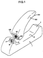
- the reference numeral 1 indicates a charger
- the reference numeral 100 indicates a cordless handset (sometimes described as a handset unit hereinafter) of a telephone set as a cordless equipment.
- the charger 1 has an outer casing 5 with a handset unit mounting base 3 on which the handset unit 100 is placed.
- the outer casing 5 comprises a inclined pillow section 7 on which a head section 104 of the outer casing 102 of the handset unit 100 is mounted, and an electromagnetic induction surface section 9, and when the head section 104 is placed on the inclined pillow section 7, a bottom surface section 106 of the outer casing 102 faces to and contacts a electromagnetic induction surface section 9, and the handset unit 100 is positioned and set on the handset unit mounting base 3.
- a printed board 11 is fixed and set with an engaging claw 13 on an internal surface of the electromagnetic induction surface section 9 of the charger 1.
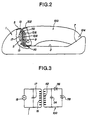
- a conductor 14 is spirally patterned, and a pattern inductor, in other words a primary side induction coil 15 having a spiral form comprising a sheet coil is planarly formed with the conductor 14.
- a sheet coil face (surface) of the printed board 11 uniformly contacts and joints to the entire internal surface of the electromagnetic induction surface section 9 when set on the electromagnetic induction surface section 9 of the printed board 11 with the engaging claw 13. This feature is very important for maintaining a gap between coils at an appropriate value during mutual induction described later.
- a capacitor 17 is mounted on a rear surface of the printed board 11. This capacitor 17 is connected, as shown in Fig. 3, in parallel to the primary side induction coil 15, and forms an LC parallel resonance circuit in the primary side together with the primary side induction coil 15. A high-frequency power 19 is connected to the LC parallel resonance circuit in the primary side.
- the printed board 108 is seated on the internal surface of the bottom surface section 106 of the handset unit 100 with the engaging claw 110.
- a conductor is spirally patterned on a surface on the printed board 108 (on a surface of the side of the bottom surface 106) like in the printed board 11, and with the conductor, a pattern inductor, in other words, a secondary side induction coil 112 having a spiral form comprising a sheet coil is formed on the surface.
- a sheet coil face (surface) of the printed board 108 is seated on the bottom surface section 106 of the printed board 108 with the engaging claw 110 and uniformly contacts and joints to the entire internal surface of the bottom surface section 106. Also this feature is one of the important requirements for maintaining a gap between coils at an appropriate value during mutual induction described later.
- a capacitor 114 is mounted on a rear surface of the printed board 108. This capacitor 114 is connected in parallel to the secondary side induction coil 112, and forms an LC parallel resonance circuit in the secondary side together with the secondary side induction coil 112. A secondary battery 118 to be charged is connected via a diode 116 to the LC parallel resonance circuit in the secondary side.
- the bottom surface section 106 of the outer casing 102 faces to and contacts flat to the electromagnetic induction surface section 9, and for this reason in the state where a handset unit has been set, the primary side induction coil 15 and the secondary side induction coil 12 face in parallel to each other with the electromagnetic induction surface section 9 of the outer casing 5 and the bottom surface section 106 of the outer casing 102 therebetween, so that a gap between the primary side induction coil 15 and the secondary side induction coil 112 is inevitably decided by a total of wall thickness of the electromagnetic induction surface section 9 and that off the bottom surface section 106.
- a double tuning circuit is formed with a combination of LC parallel resonance circuits formed in the charger 1 and the handset unit 100 respectively, and power transmission from the charger 1 to the handset unit 100 is executed by means of mutual induction by the double tuning circuit.
- each of the primary side induction coil 15 and the secondary side induction coil 112 is formed with a sheet coil, construction of the coil itself and mounting construction for the coil do not become complicated, and with the induction coils, mutual induction is efficiently performed with a large magnetic connection area with an appropriate gap at which the critical connection state can be achieved and without making larger size and weight of the coil.
- the critical connection state is achieved depending on the magnetic connection coefficient, so that, by setting a gap between the primary side induction coil 15 and the secondary side induction coil 112 to on appropriate value, the critical connection state can be obtained, and efficient power transmission can be performed with the maximum and single peak frequency characteristics.
- Fig. 5 shows the inter-coil gap/loss level characteristics for the harmonic frequency. This graph shows that, in a case where the inter-coil gap is 6 mm, the loss level is minimum with excellent mutual induction state, and that, in a case where the inter-coil gap is more than or less than 6 mm, the loss level increases with the mutual induction state degraded.
- the appropriate gap enabling the critical connection state is 6 mm, and wall thickness of the electromagnetic induction surface section 9 and that of the bottom surface section 106 should be set to 3 mm respectively.
- Sheet coils of the primary side induction coil 15 and the secondary side induction coil 112 respectively are spirally patterned on surfaces of the printed boards 11 and 108, so that a large planary magnetic field in obtained with a small space and a large magnetic connection area can be obtained without making larger size and weight of the coils.
- this sheet coil is formed with a pattern inductor provided on a printed board, and the pattern inductors are mass-produced with stable performance and low cost by making use of the printed board production technology, so that the sheet coil, in other words, the primary side induction coil 15 and secondary side induction coil 112 are formed with low cost products with stable quality, which allows cost reduction.
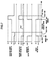
- Fig. 6 shows electric circuits in a noncontact charger as well as in a cordless equipment (handset unit). It should be noted that the same reference numerals as those used in Fig. 1 to Fig. 3 are assigned to portions corresponding to those in Fig. 1 to Fig. 3.
- the noncontact charger 1 comprises an LC parallel resonance circuit 21 formed with a primary side induction coil 15 (L 1 ) and a capacitor 17 (C 2 ), a DC current source 23 obtained from, for instance, an AC adapter, an oscillation circuit 25 comprising, for instance, a CR oscillator, a resonance circuit driving transistor 27 (Q 1 ) for driving the LC parallel resonance circuit 21 at a high frequency when a high-frequency signal outputted from the oscillation circuit 25 is given to a gate terminal, a resonance state switching transistor 31 (Q 2 ) for switching a oscillation voltage level in the LC parallel resonance circuit 21 between a high level and a low level by opening and closing a circuit for a partial voltage resistance 29 (R 21 ), a detection circuit 33 (D 1 , C 5 , R 6 ) connected to the LC parallel resonance circuit 21 and outputting amplitude of an oscillation frequency signal as a voltage signal Va, a variable amplifier 35 for amplifying an output voltage Va from the detection circuit 33, and a comparator 37 (OP 2
- the comparator 37 determines that the primary side induction coil 15 is not in the mutual conduction state, and outputs an ON signal, and otherwise, namely when the voltage Vb is not larger than the reference value Vref for comparison, the comparator 37 determines that the primary side induction coil is in the mutual induction state, and outputs an OFF signal.
- the ON or OFF signal described above namely a determination signal (output voltage) Vc is inputted via a delay circuit 43 comprising a resistance 39 (R 20 ) and a capacitor 41 (C 5 ) into a gate terminal of the resonance state switching transistor 31.
- the resonance state switching transistor 31 When the primary side induction coil 15 is not in the mutual induction state, namely in the idle state where the handset unit 100 has not been set in the charger 1, the resonance state switching transistor 31 is set in the ON state, sets a oscillation voltage level in the LC parallel resonance circuit 21 to a low level, while, when the primary side induction coil 15 is in the mutual induction state, namely in the state where the handset unit 100 has been set in the charger 1, the transistor 31 is set in the OFF state, and sets a oscillation voltage level in the LC parallel resonance circuit 21 to a high level.
- the variable amplifier 35 in this embodiment comprises a non-inverting amplifier which is an operating amplifier (OP 1 ), has a partial voltage resistance 49 (R 18 ) selectively connected by a transistor 47 (Q 3 ) to any of the offset voltage circuit 45 (R 15 to R 19 ), and selectively lowers the offset voltage Vd with this partial voltage resistance 49.
- OP 1 operating amplifier
- R 18 partial voltage resistance 49
- Q 3 transistor 47
- the above-described ON/OFF signal (Vc) outputted from the comparator 37 is given to a gate terminal of the transistor 47.
- a return resistance circuit 51 (R 7 to R 10 ) of the variable amplifier 35 is also provided in a return resistance circuit 51 (R 7 to R 10 ) of the variable amplifier 35 .
- a partial voltage resistance 55 (R 9 ) selectively connected by a transistor 53 (Q 4 ) to the circuit, and the amplification factor G is selectively made larger by this partial voltage resistance 55.
- the above-described ON/OFF signal (Vc) outputted from the comparator 37 is given to a gate terminal of the transistor 53.
- the handset unit 100 has a an LC parallel resonance circuit 120 comprising a secondary side induction coil 112 (L 2 ) and a capacitor 114 (C 7 ), a secondary battery 118, and a double voltage rectification circuit 130 comprising two diodes 122 (D 2 ), 124 (D 3 ) mutually-inversively connected to each other and provided between the resonance circuit 120 and the secondary battery 118 and two smoothing capacitors 126 (C 9 ) and 128 (C 8 ).
- LC parallel resonance circuit 120 comprising a secondary side induction coil 112 (L 2 ) and a capacitor 114 (C 7 ), a secondary battery 118, and a double voltage rectification circuit 130 comprising two diodes 122 (D 2 ), 124 (D 3 ) mutually-inversively connected to each other and provided between the resonance circuit 120 and the secondary battery 118 and two smoothing capacitors 126 (C 9 ) and 128 (C 8 ).
- signs R 1 to R 22 indicate a resistance respectively
- C 1 to C 6 indicate a capacitor
- Q 1 to Q 4 indicates a transistor respectively
- D 1 to D 3 indicates a diode respectively.
- a voltage between terminals of the secondary battery 118 looks like 1/2 of the actual value when viewed from the input side, and with this feature, even if the oscillation level is low as described above, when the handset unit 100 is set on the charger, a charging current flows without fail.
- oscillation amplitude namely oscillation level in the resonance circuit 21 further lowers to, for instance, around 1 Vp-p.
- an output voltage Va from the detection circuit 33 is around 1.0 V
- each of the transistors 47, 53 is immediately turned OFF with the offset voltage Vd in the variable amplifier 35 raised to around 4 V, and the amplification factor G of the variable amplifier 35 is lowered to around 3 V.
- an offset voltage in the variable amplifier 35 is switched according to whether an oscillation voltage level in the resonance circuit 21 is a high level or a low level, and with only one reference value for comparison Vref for the comparison 37, irrespective of whether an oscillation voltage level in the resonance circuit 21 is a high level or a low level, whether the primary side induction coil 15 is in the mutual induction state or not, namely whether the handset unit 100 is set on the charger 1 or not can accurately be determined.
- an amplification factor for the variable 35 amplifier in a state other than the mutual induction state is made larger as compared to that in the mutual induction state, so that an output voltage from the variable amplifier largely changes in response to change in oscillation amplitude, and in the idle state where mutual induction state is not effected and an oscillation voltage level in the resonance circuit is at a low level, even if change in oscillation amplifier changes only a little when the handset unit 100 is set in the charger 1, the fact that the handset unit 100 has been set can accurately be detected by the comparator 37.
- Fig. 8 shows an electric circuit according to another embodiment of the noncontact charger and cordless equipment (handset unit) according to the present invention. It should be noted that, in Fig. 8, the same reference numerals are assigned to portions corresponding to those in Fig. 6 and description thereof is omitted herein.
- An output voltage Va from the detection circuit 33 in each state is the same as that in the embodiment described above, and this output voltage Va is inputted into a first comparator 61 as well as into a second comparator 63.
- the first comparator 61 compares an output voltage Va to the first reference value for comparison Vref1, and outputs a low signal when Va is larger than Vref1 (Va > Vref1), and otherwise outputs a high signal.
- the first reference value for comparison Vref1 is set to around 1.2 V
- the first comparator 61 outputs a high signal only when the handset unit 100 is set on the charger 1 in the idle state, and outputs a low signal in the idle state, when charging with a high level output, and when the handset unit 100 is removed from the charger 1 in the charging state with a high level output.
- the second comparator 63 compares the output voltage Va to a second reference value for comparison Vref2 larger than the first reference value for comparison Vref1, and when Va is larger than Vref2 (Va > Vref2), outputs a low signals, and otherwise output a high signal.
- the second reference value for comparison Vref2 is set to around 4 V, the second comparator 63 outputs a low signal only when the handset unit 100 is removed from the charger 1 in the charging state with high level output, and outputs a low signal, when the handset unit 100 is set in the charger 1 in the idle state, or when charging is executed with high level output.
- Output signals from the first comparator 61 and second comparator 63 are inputted to a two-input type of NOR gate 65 and an AND gate 76 respectively.
- An output signal from the NOR gate 65 is inputted into a reset terminal of the D-latch circuit 69, and an output signal from the AND gate 67 is inputted to a clock terminal of the D-latch circuit 69.
- the D-latch circuit 69 inverts an inverted Q output signal from ON to OFF according to shift of a signal inputted into the clock terminal from low to high, and also inverts the inverted Q output signal from OFF to ON according to reset input.
- This inverted Q output signal is inputted to a gate terminal of the resonance state switching transistor 31 as a determination signal indicating whether the primary side induction coil 15 is in the mutual induction state or not.
- an oscillation level in the resonance circuit 21 lowers in the idle state, so that, even if a metallic conductor is placed by mistake on the charger 1, substantial induction heating does not occur with wasteful power consumption reduced, and whether the handset unit 100 has been set in the charger 1 or not can accurately be detected without requiring any specific sensor.
- each of the primary side induction coil and secondary side induction coil provided in a charger and a cordless equipment respectively comprises a sheet coil, so that construction of the coil itself and the mounting construction thereof are not complicated, and with the induction coils, mutual induction is efficiently executed with a appropriate gap and a large magnetic connection area without making size and weight of the coil larger, and wasteful power consumption is reduced and charging is executed at a high speed.
- the non-contact charging device by setting a gap between the primary side induction coil and secondary side induction coil to an appropriate value, the critical connection state is achieved and efficient power transmission is executed with the maximum and signal peak frequency characteristics, and also with this feature, wasteful power consumption is reduced and charging is executed at a high speed.
- a sheet coil is spirally patterned on one plane, so that a large and flat magnetic field is obtained with a small space and a large magnetic connection area is obtained without making larger size and weight of each coil, and also with this feature, wasteful power consumption is reduced and charging is executed at a high speed.
- a sheet coil comprises a pattern inductor patterned on a printed board, and as pattern inductors can be mass-produced with stable performance and high productivity and also with low cost, the sheet coil can comprises a low cost product with excellent and stable quality.
- the charger according to the present invention functions as the noncontact charger according to the present invention, so that wasteful power consumption is reduced and charging is executed at a high speed.
- the cordless equipment according to the present invention functions as a cordless equipment in the noncontact charging device according to the present invention, so that wasteful power consumption is reduced and charging is executed at a high speed.
- the noncontact charger when a cordless equipment is set in the charger, mutual induction state is detected by the mutual induction state detecting means and an oscillation voltage level in the resonance circuit is set by the resonance state switching means to a high level, and if a cordless equipment is not set in the charger, the mutual induction state detecting means detects that the mutual induction state has not been effected, and a oscillation voltage level in the resonance circuit is set by the resonance state switching means to a low level, so that, even if a metallic conductor is placed by mistake on the charger in the idle state which is different from the mutual induction state, substantial induction heating does not occur with wasteful power consumption reduced, and whether any cordless equipment is placed on the charger or not can accurately be detected without requiring any specific sensor.
- an offset voltage in the variable amplifier is switched according to whether a oscillation voltage level in the resonance circuit is at a high level or a low level, so that, even with only one reference value for comparison, whether the primary side induction coil is in the mutual induction state or not can accurately be determined irrespective of whether a oscillation voltage level in the resonance circuit is high or low.
- a determination signal is given to the variable amplifier, and an amplification factor for the variable amplifier in a state other than the mutual induction state is made larger as compared to that in the mutual induction state, so that even if oscillation amplitude changes only a little when a cordless equipment is set in the charger in the idle state where a cordless equipment is not set in the charger, the fact that the cordless equipment has been set can accurately be detected by the compactor.
- a determination signal indicating whether the induction coil is in the mutual induction state or not is outputted with a combination of output signals from the first comparator and second comparator, and for this reason whether a cordless equipment has been set on the charger or not can accurately be detected without requiring any specific sensor.
- a voltage between terminals of the secondary battery seems to be 1/2 of the actual value when viewed from the input side because of existence of the double voltage rectification circuit, so that, even if an oscillation level in the stand-by state is low, a charging current flows without fail when a cordless equipment is set in the charge, and the fact that the cordless equipment has been set in the charger can accurately be detected in the charger side according to change in oscillation amplitude.
- the invention may e.g. be summarized as follows:
- Capacitors are connected in parallel to a primary side induction coil in a charger 1 and a secondary side induction coil in a cordless equipment (handset unit) respectively, and LC parallel resonance circuits are formed in the charger and the cordless equipment respectively with this parallel connection.
- Each of the primary side induction coil and secondary side induction coil is formed with a sheet coil, and the sheet coils are arranged and fixed in the charger and the cordless equipment respectively so that the sheet coils face to each other with a prespecified gap in the charging state where the cordless equipment has been set in the charger.
Landscapes
- Engineering & Computer Science (AREA)
- Power Engineering (AREA)
- Computer Networks & Wireless Communication (AREA)
- Charge And Discharge Circuits For Batteries Or The Like (AREA)
- Secondary Cells (AREA)
- Mobile Radio Communication Systems (AREA)
Applications Claiming Priority (3)
| Application Number | Priority Date | Filing Date | Title |
|---|---|---|---|
| JP17397696 | 1996-07-03 | ||
| JP8173976A JPH1023677A (ja) | 1996-07-03 | 1996-07-03 | 無接点充電装置、充電器、コードレス機器および無接点充電器 |
| JP173976/96 | 1996-07-03 |
Publications (2)
| Publication Number | Publication Date |
|---|---|
| EP0817351A2 true EP0817351A2 (fr) | 1998-01-07 |
| EP0817351A3 EP0817351A3 (fr) | 1999-07-07 |
Family
ID=15970514
Family Applications (1)
| Application Number | Title | Priority Date | Filing Date |
|---|---|---|---|
| EP97111174A Withdrawn EP0817351A3 (fr) | 1996-07-03 | 1997-07-03 | Dispositif de charge sans contact, chargeur, appareils électriques sans fil, et chargeur sans contact |
Country Status (3)
| Country | Link |
|---|---|
| US (1) | US5929598A (fr) |
| EP (1) | EP0817351A3 (fr) |
| JP (1) | JPH1023677A (fr) |
Cited By (11)
| Publication number | Priority date | Publication date | Assignee | Title |
|---|---|---|---|---|
| EP1022840A2 (fr) | 1999-01-20 | 2000-07-26 | Perdix Oy | Contrôleur pour un chargeur inductif de batterie |
| WO2002015375A1 (fr) * | 2000-08-14 | 2002-02-21 | Alstom | Unite d'alimentation d'energie destinee a transmettre une energie auxiliaire a un dispositif electrique |
| WO2002042620A1 (fr) * | 2000-11-21 | 2002-05-30 | Robert Bosch Gmbh | Moteur a combustion comportant au moins un cylindre dans lequel est loge un piston a mouvement alternatif |
| WO2002071423A1 (fr) | 2001-03-02 | 2002-09-12 | Koninklijke Philips Electronics N.V. | Systeme de couplage inductif avec compensation capacitive en parallele de l'auto-inductance mutuelle entre les bobines primaire et secondaire |
| EP1303022A1 (fr) * | 2001-10-12 | 2003-04-16 | The Swatch Group Management Services AG | Chargeur inductif pour objet portatif électronique tel que, notamment, une pièce d'horlogerie du type montre-bracelet |
| GB2393860A (en) * | 2002-09-27 | 2004-04-07 | Zap Wireless Technologies Ltd | Variable positioning of devices being inductively charged |
| EP1646122A1 (fr) * | 2004-10-06 | 2006-04-12 | Nokia Corporation | Panneau à circuit imprimé multicouche portant un circuit de charge de batterie et une bobine d'induction |
| WO2005106901A3 (fr) * | 2004-05-04 | 2006-05-26 | Philips Intellectual Property | Dispositif d'alimentation sans fil, charge d'excitation, systeme sans fil et procede de transfert d'energie sans fil |
| US7263388B2 (en) * | 2001-06-29 | 2007-08-28 | Nokia Corporation | Charging system for portable equipment |
| WO2008035248A2 (fr) | 2006-09-18 | 2008-03-27 | Philips Intellectual Property & Standards Gmbh | Appareil, système et procédé permettant le transfert d'énergie électromagnétique |
| EP2878291A4 (fr) * | 2012-07-24 | 2016-04-27 | Lover Health Science And Technology Co Ltd | Masseur sexuel du type à molette de souris |
Families Citing this family (60)
| Publication number | Priority date | Publication date | Assignee | Title |
|---|---|---|---|---|
| DE69831226T2 (de) * | 1997-11-20 | 2006-03-30 | Seiko Epson Corp. | Elektronische vorrichtung |
| US6731071B2 (en) * | 1999-06-21 | 2004-05-04 | Access Business Group International Llc | Inductively powered lamp assembly |
| US7385357B2 (en) * | 1999-06-21 | 2008-06-10 | Access Business Group International Llc | Inductively coupled ballast circuit |
| US7126450B2 (en) * | 1999-06-21 | 2006-10-24 | Access Business Group International Llc | Inductively powered apparatus |
| US6825620B2 (en) * | 1999-06-21 | 2004-11-30 | Access Business Group International Llc | Inductively coupled ballast circuit |
| US7612528B2 (en) | 1999-06-21 | 2009-11-03 | Access Business Group International Llc | Vehicle interface |
| US9425638B2 (en) | 1999-11-01 | 2016-08-23 | Anthony Sabo | Alignment independent and self-aligning inductive power transfer system |
| KR100566220B1 (ko) * | 2001-01-05 | 2006-03-29 | 삼성전자주식회사 | 무접점 배터리 충전기 |
| CH713523B1 (fr) * | 2001-11-26 | 2018-09-14 | Ebauchesfabrik Eta Ag | Objet électronique portatif tel qu'une pièce d'horlogerie susceptible d'être porté au poignet. |
| US7392068B2 (en) * | 2002-03-01 | 2008-06-24 | Mobilewise | Alternative wirefree mobile device power supply method and system with free positioning |
| US6913477B2 (en) * | 2002-03-01 | 2005-07-05 | Mobilewise, Inc. | Wirefree mobile device power supply method & system with free positioning |
| GB2398784B (en) * | 2003-02-26 | 2005-07-27 | Babraham Inst | Removal and modification of the immunoglobulin constant region gene cluster of a non-human mammal |
| JP2005143181A (ja) | 2003-11-05 | 2005-06-02 | Seiko Epson Corp | 非接触電力伝送装置 |
| KR20040072581A (ko) * | 2004-07-29 | 2004-08-18 | (주)제이씨 프로텍 | 전자기파 증폭중계기 및 이를 이용한 무선전력변환장치 |
| US7462951B1 (en) | 2004-08-11 | 2008-12-09 | Access Business Group International Llc | Portable inductive power station |
| US7408324B2 (en) * | 2004-10-27 | 2008-08-05 | Access Business Group International Llc | Implement rack and system for energizing implements |
| JP2006230129A (ja) * | 2005-02-18 | 2006-08-31 | Nanao Corp | 非接触電力供給装置 |
| CN100420120C (zh) * | 2005-07-21 | 2008-09-17 | 张定港 | 媒体播放器的感应式充电装置 |
| US9132058B2 (en) | 2006-02-01 | 2015-09-15 | LELO Inc. | Rechargeable personal massager |
| JP2007321425A (ja) * | 2006-05-31 | 2007-12-13 | Matsushita Electric Works Ltd | 電気錠 |
| US7411363B2 (en) * | 2006-06-26 | 2008-08-12 | Lam Dat D | Conservation of electrical energy and electro-magnetic power in motor, generator, and product components |
| JP2008104295A (ja) * | 2006-10-19 | 2008-05-01 | Voltex:Kk | 非接触電源装置 |
| MX2009008011A (es) * | 2007-01-29 | 2010-02-18 | Powermat Ltd | Acoplamiento de energia sin clavija y metodo para controlar la transferenca de la energia atraves de un acoplamiento inductivo. |
| JP4649430B2 (ja) * | 2007-03-20 | 2011-03-09 | セイコーエプソン株式会社 | 非接触電力伝送装置 |
| CN102106054A (zh) | 2007-03-22 | 2011-06-22 | 鲍尔马特有限公司 | 信号传递系统 |
| US10463252B2 (en) * | 2007-03-27 | 2019-11-05 | Siemens Medical Solutions Usa, Inc. | Interface for component identification, communication and power supply between interchangeable system components |
| DE102007060811A1 (de) * | 2007-09-01 | 2009-03-05 | Maquet Gmbh & Co. Kg | Vorrichtung und Verfahren zur drahtlosen Energie- und/oder Datenübertragung zwischen einem Quellgerät und mindestens einem Zielgerät |
| US10068701B2 (en) | 2007-09-25 | 2018-09-04 | Powermat Technologies Ltd. | Adjustable inductive power transmission platform |
| AU2008303118A1 (en) * | 2007-09-25 | 2009-04-02 | Powermat Technologies Ltd. | Inductive power transmission platform |
| US8193769B2 (en) * | 2007-10-18 | 2012-06-05 | Powermat Technologies, Ltd | Inductively chargeable audio devices |
| US8536737B2 (en) * | 2007-11-19 | 2013-09-17 | Powermat Technologies, Ltd. | System for inductive power provision in wet environments |
| US20100219183A1 (en) * | 2007-11-19 | 2010-09-02 | Powermat Ltd. | System for inductive power provision within a bounding surface |
| US8421267B2 (en) * | 2008-03-10 | 2013-04-16 | Qualcomm, Incorporated | Packaging and details of a wireless power device |
| US9960640B2 (en) | 2008-03-17 | 2018-05-01 | Powermat Technologies Ltd. | System and method for regulating inductive power transmission |
| KR20100130215A (ko) * | 2008-03-17 | 2010-12-10 | 파우워매트 엘티디. | 유도송전장치 |
| US9337902B2 (en) | 2008-03-17 | 2016-05-10 | Powermat Technologies Ltd. | System and method for providing wireless power transfer functionality to an electrical device |
| US9331750B2 (en) | 2008-03-17 | 2016-05-03 | Powermat Technologies Ltd. | Wireless power receiver and host control interface thereof |
| US9960642B2 (en) | 2008-03-17 | 2018-05-01 | Powermat Technologies Ltd. | Embedded interface for wireless power transfer to electrical devices |
| US8320143B2 (en) * | 2008-04-15 | 2012-11-27 | Powermat Technologies, Ltd. | Bridge synchronous rectifier |
| CA2726552A1 (fr) * | 2008-06-02 | 2009-12-10 | Powermat Ltd. | Prises de courant montees sur des appareils electriques |
| US8188619B2 (en) | 2008-07-02 | 2012-05-29 | Powermat Technologies Ltd | Non resonant inductive power transmission system and method |
| US11979201B2 (en) | 2008-07-02 | 2024-05-07 | Powermat Technologies Ltd. | System and method for coded communication signals regulating inductive power transmissions |
| US8981598B2 (en) | 2008-07-02 | 2015-03-17 | Powermat Technologies Ltd. | Energy efficient inductive power transmission system and method |
| AU2009269574A1 (en) * | 2008-07-08 | 2010-01-14 | Powermat Technologies Ltd. | Display device |
| MY159639A (en) * | 2008-07-09 | 2017-01-13 | Access Business Group Int Llc | Wireless charging system |
| AU2009297963A1 (en) * | 2008-09-23 | 2010-04-01 | Powermat Technologies Ltd. | Combined antenna and inductive power receiver |
| USD611898S1 (en) | 2009-07-17 | 2010-03-16 | Lin Wei Yang | Induction charger |
| USD611899S1 (en) | 2009-07-31 | 2010-03-16 | Lin Wei Yang | Induction charger |
| USD611900S1 (en) | 2009-07-31 | 2010-03-16 | Lin Wei Yang | Induction charger |
| US8174233B2 (en) * | 2009-10-08 | 2012-05-08 | Etymotic Research, Inc. | Magnetically coupled battery charging system |
| US20110099507A1 (en) * | 2009-10-28 | 2011-04-28 | Google Inc. | Displaying a collection of interactive elements that trigger actions directed to an item |
| US9615994B2 (en) | 2011-07-06 | 2017-04-11 | LELO Inc. | Motion-based control for a personal massager |
| DE112012006861B4 (de) * | 2012-08-31 | 2024-01-11 | Siemens Aktiengesellschaft | Batterieladesystem und Verfahren zum kabellosen Laden einer Batterie |
| US9178361B2 (en) * | 2012-09-27 | 2015-11-03 | ConvenientPower, Ltd. | Methods and systems for detecting foreign objects in a wireless charging system |
| KR102052590B1 (ko) * | 2012-11-22 | 2019-12-05 | 삼성에스디아이 주식회사 | 배터리 관리 시스템 및 그 구동 방법 |
| JP6812912B2 (ja) * | 2017-06-26 | 2021-01-13 | Tdk株式会社 | Fet駆動回路 |
| ES3050085T3 (en) | 2017-07-07 | 2025-12-19 | Neuroderm Ltd | Device for subcutaneous delivery of fluid medicament |
| US20230123806A1 (en) | 2017-07-07 | 2023-04-20 | Neuroderm, Ltd. | Device for subcutaneous delivery of fluid medicament |
| USD881122S1 (en) | 2019-02-19 | 2020-04-14 | Kenu, Inc. | Power bank with kickstand |
| US11431201B2 (en) * | 2019-09-16 | 2022-08-30 | Analog Devices International Unlimited Company | Techniques for improved wireless energy transmission efficiency |
Family Cites Families (12)
| Publication number | Priority date | Publication date | Assignee | Title |
|---|---|---|---|---|
| US4031449A (en) * | 1975-11-20 | 1977-06-21 | Arthur D. Little, Inc. | Electromagnetically coupled battery charger |
| JPS6057189B2 (ja) * | 1977-06-30 | 1985-12-13 | 新神戸電機株式会社 | 蓄電池 |
| US4202031A (en) * | 1978-11-01 | 1980-05-06 | General Electric Company | Static inverter employing an assymetrically energized inductor |
| JP3303306B2 (ja) * | 1991-09-03 | 2002-07-22 | 松下電器産業株式会社 | 電磁誘導充電回路 |
| US5157319A (en) * | 1991-09-27 | 1992-10-20 | Electric Power Research Institute | Contactless battery charging system |
| US5327065A (en) * | 1992-01-22 | 1994-07-05 | Hughes Aircraft Company | Hand-held inductive charger having concentric windings |
| JPH05300662A (ja) * | 1992-04-23 | 1993-11-12 | Matsushita Electric Works Ltd | 充電装置 |
| JP3309499B2 (ja) * | 1993-06-14 | 2002-07-29 | ソニー株式会社 | 無接点電力供給装置 |
| JP3409145B2 (ja) * | 1993-07-26 | 2003-05-26 | 任天堂株式会社 | 小型電気機器 |
| US5490053A (en) * | 1993-09-30 | 1996-02-06 | Apple Computer, Inc. | Methods and apparatus for auxiliary trickle power supply |
| JPH07170312A (ja) * | 1993-12-16 | 1995-07-04 | Matsushita Electric Ind Co Ltd | コードレス電話装置 |
| JP2671809B2 (ja) * | 1994-06-30 | 1997-11-05 | 日本電気株式会社 | 非接触型充電装置 |
-
1996
- 1996-07-03 JP JP8173976A patent/JPH1023677A/ja active Pending
-
1997
- 1997-07-03 US US08/888,122 patent/US5929598A/en not_active Expired - Lifetime
- 1997-07-03 EP EP97111174A patent/EP0817351A3/fr not_active Withdrawn
Cited By (22)
| Publication number | Priority date | Publication date | Assignee | Title |
|---|---|---|---|---|
| DE19901983A1 (de) * | 1999-01-20 | 2000-08-10 | Perdix Oy Helsinki | Steuervorrichtung für einen induktiven Akkulader |
| EP1022840A3 (fr) * | 1999-01-20 | 2001-04-04 | Perdix Oy | Contrôleur pour un chargeur inductif de batterie |
| EP1022840A2 (fr) | 1999-01-20 | 2000-07-26 | Perdix Oy | Contrôleur pour un chargeur inductif de batterie |
| US7221066B2 (en) | 2000-08-14 | 2007-05-22 | Alstom | Energy supply unit for transmitting auxiliary energy to an electrical device |
| WO2002015375A1 (fr) * | 2000-08-14 | 2002-02-21 | Alstom | Unite d'alimentation d'energie destinee a transmettre une energie auxiliaire a un dispositif electrique |
| WO2002042620A1 (fr) * | 2000-11-21 | 2002-05-30 | Robert Bosch Gmbh | Moteur a combustion comportant au moins un cylindre dans lequel est loge un piston a mouvement alternatif |
| WO2002071423A1 (fr) | 2001-03-02 | 2002-09-12 | Koninklijke Philips Electronics N.V. | Systeme de couplage inductif avec compensation capacitive en parallele de l'auto-inductance mutuelle entre les bobines primaire et secondaire |
| US6498456B2 (en) | 2001-03-02 | 2002-12-24 | Koninklijke Philips Electronics N.V | Inductive coupling system with capacitive parallel compensation of the mutual self-inductance between the primary and the secondary windings |
| KR100888465B1 (ko) | 2001-03-02 | 2009-03-11 | 코닌클리케 필립스 일렉트로닉스 엔.브이. | 1차 권선과 2차 권선 사이의 상호 자기 인덕턴스의 용량성 병렬 보상을 가지는 유도성 커플링 시스템, 및 재충전가능한 전기 제품과 스탠드의 결합 |
| US7263388B2 (en) * | 2001-06-29 | 2007-08-28 | Nokia Corporation | Charging system for portable equipment |
| EP1303022A1 (fr) * | 2001-10-12 | 2003-04-16 | The Swatch Group Management Services AG | Chargeur inductif pour objet portatif électronique tel que, notamment, une pièce d'horlogerie du type montre-bracelet |
| WO2003034569A3 (fr) * | 2001-10-12 | 2003-12-04 | Swatch Group Man Serv Ag | Chargeur electrique inductif pour objet portatif electronique tel que, notamment, une piece d'horlogerie du type montre-bracelet |
| GB2393860B (en) * | 2002-09-27 | 2006-02-15 | Zap Wireless Technologies Ltd | Improvements relating to retention of rechargeable devices |
| GB2393860A (en) * | 2002-09-27 | 2004-04-07 | Zap Wireless Technologies Ltd | Variable positioning of devices being inductively charged |
| US7518337B2 (en) | 2002-09-27 | 2009-04-14 | Access Business Group International Llc | Retention of inductively rechargeable devices on an inductive charger |
| WO2005106901A3 (fr) * | 2004-05-04 | 2006-05-26 | Philips Intellectual Property | Dispositif d'alimentation sans fil, charge d'excitation, systeme sans fil et procede de transfert d'energie sans fil |
| EP1646122A1 (fr) * | 2004-10-06 | 2006-04-12 | Nokia Corporation | Panneau à circuit imprimé multicouche portant un circuit de charge de batterie et une bobine d'induction |
| WO2008035248A2 (fr) | 2006-09-18 | 2008-03-27 | Philips Intellectual Property & Standards Gmbh | Appareil, système et procédé permettant le transfert d'énergie électromagnétique |
| WO2008035248A3 (fr) * | 2006-09-18 | 2008-07-03 | Philips Intellectual Property | Appareil, système et procédé permettant le transfert d'énergie électromagnétique |
| CN101517666B (zh) * | 2006-09-18 | 2012-01-04 | 皇家飞利浦电子股份有限公司 | 用于实现电磁能量传递的装置、系统和方法 |
| US9520225B2 (en) | 2006-09-18 | 2016-12-13 | Koninklijke Philips N.V. | Apparatus, a system and a method for enabling electromagnetic energy transfer |
| EP2878291A4 (fr) * | 2012-07-24 | 2016-04-27 | Lover Health Science And Technology Co Ltd | Masseur sexuel du type à molette de souris |
Also Published As
| Publication number | Publication date |
|---|---|
| US5929598A (en) | 1999-07-27 |
| EP0817351A3 (fr) | 1999-07-07 |
| JPH1023677A (ja) | 1998-01-23 |
Similar Documents
| Publication | Publication Date | Title |
|---|---|---|
| US5929598A (en) | Noncontact charging device, charger, cordless electric equipment, and noncontact charger | |
| US12456886B2 (en) | Methods and circuitry for mitigating saturation in wireless power systems | |
| US7847438B2 (en) | Power transmission device, electronic instrument, and waveform monitoring circuit | |
| US7812481B2 (en) | Power transmission control device, power transmission device, electronic instrument, and non-contact power transmission system | |
| EP1022840B1 (fr) | Contrôleur pour un chargeur inductif de batterie | |
| KR102224451B1 (ko) | 전력 수신기 및 전력 전송기 | |
| US8004118B2 (en) | Power transmission control device, power transmitting device, electronic instrument, and non-contact power transmission system | |
| CN102377251B (zh) | 电力传送系统 | |
| US20020110013A1 (en) | Coreless superthin PCB transformer and non-contact battery charger using the same | |
| JPH0879976A (ja) | 非接触型充電器 | |
| JPH06178464A (ja) | 非接触電力供給装置 | |
| JPH0837121A (ja) | 給電装置 | |
| CN104104155A (zh) | 馈电单元和馈电系统 | |
| JPH08163792A (ja) | 電磁誘導コイルの駆動回路及び該駆動回路を用いた充電装置 | |
| KR102205359B1 (ko) | 무선 전력 전송 시스템에서 이물질 감지 장치 및 방법 | |
| JP7477347B2 (ja) | ワイヤレス送電装置及びワイヤレス電力伝送システム | |
| JP7477346B2 (ja) | ワイヤレス送電装置及びワイヤレス電力伝送システム | |
| KR200217303Y1 (ko) | 무선 충전 장치 | |
| US11967836B2 (en) | Harmonic current monitoring in a wireless power system | |
| KR102136667B1 (ko) | 무선 전력 전송 시스템에서 이물질 감지 장치 및 방법 | |
| Choi et al. | A new contactless battery charger for portable telecommunication/computing electronics | |
| JPH08205432A (ja) | 非接触型電力伝送装置 | |
| JPH08103028A (ja) | 非接触充電器 | |
| JP3206244B2 (ja) | コードレス電話機 | |
| KR20210014712A (ko) | 무선 전력 전송 시스템에서 이물질 감지 장치 및 방법 |
Legal Events
| Date | Code | Title | Description |
|---|---|---|---|
| PUAI | Public reference made under article 153(3) epc to a published international application that has entered the european phase |
Free format text: ORIGINAL CODE: 0009012 |
|
| AK | Designated contracting states |
Kind code of ref document: A2 Designated state(s): AT BE CH DE DK ES FI FR GB GR IE IT LI LU MC NL PT SE |
|
| PUAL | Search report despatched |
Free format text: ORIGINAL CODE: 0009013 |
|
| AK | Designated contracting states |
Kind code of ref document: A3 Designated state(s): AT BE CH DE DK ES FI FR GB GR IE IT LI LU MC NL PT SE |
|
| AKX | Designation fees paid | ||
| REG | Reference to a national code |
Ref country code: DE Ref legal event code: 8566 |
|
| STAA | Information on the status of an ep patent application or granted ep patent |
Free format text: STATUS: THE APPLICATION IS DEEMED TO BE WITHDRAWN |
|
| 18D | Application deemed to be withdrawn |
Effective date: 20000108 |