EP0824270A2 - Procédé pour le montage d'une pluralité de pièces électroniques sur un panneau de circuit - Google Patents
Procédé pour le montage d'une pluralité de pièces électroniques sur un panneau de circuit Download PDFInfo
- Publication number
- EP0824270A2 EP0824270A2 EP97113530A EP97113530A EP0824270A2 EP 0824270 A2 EP0824270 A2 EP 0824270A2 EP 97113530 A EP97113530 A EP 97113530A EP 97113530 A EP97113530 A EP 97113530A EP 0824270 A2 EP0824270 A2 EP 0824270A2
- Authority
- EP
- European Patent Office
- Prior art keywords
- adhesive layer
- adhesive
- electrodes
- electrode surface
- electronic parts
- Prior art date
- Legal status (The legal status is an assumption and is not a legal conclusion. Google has not performed a legal analysis and makes no representation as to the accuracy of the status listed.)
- Granted
Links
Images


Classifications
-
- H—ELECTRICITY
- H05—ELECTRIC TECHNIQUES NOT OTHERWISE PROVIDED FOR
- H05K—PRINTED CIRCUITS; CASINGS OR CONSTRUCTIONAL DETAILS OF ELECTRIC APPARATUS; MANUFACTURE OF ASSEMBLAGES OF ELECTRICAL COMPONENTS
- H05K3/00—Apparatus or processes for manufacturing printed circuits
- H05K3/30—Assembling printed circuits with electric components, e.g. with resistors
- H05K3/32—Assembling printed circuits with electric components, e.g. with resistors electrically connecting electric components or wires to printed circuits
- H05K3/321—Assembling printed circuits with electric components, e.g. with resistors electrically connecting electric components or wires to printed circuits by conductive adhesives
- H05K3/323—Assembling printed circuits with electric components, e.g. with resistors electrically connecting electric components or wires to printed circuits by conductive adhesives by applying an anisotropic conductive adhesive layer over an array of pads
-
- H—ELECTRICITY
- H10—SEMICONDUCTOR DEVICES; ELECTRIC SOLID-STATE DEVICES NOT OTHERWISE PROVIDED FOR
- H10P—GENERIC PROCESSES OR APPARATUS FOR THE MANUFACTURE OR TREATMENT OF DEVICES COVERED BY CLASS H10
- H10P72/00—Handling or holding of wafers, substrates or devices during manufacture or treatment thereof
- H10P72/70—Handling or holding of wafers, substrates or devices during manufacture or treatment thereof for supporting or gripping
- H10P72/74—Handling or holding of wafers, substrates or devices during manufacture or treatment thereof for supporting or gripping using temporarily an auxiliary support
-
- H—ELECTRICITY
- H10—SEMICONDUCTOR DEVICES; ELECTRIC SOLID-STATE DEVICES NOT OTHERWISE PROVIDED FOR
- H10W—GENERIC PACKAGES, INTERCONNECTIONS, CONNECTORS OR OTHER CONSTRUCTIONAL DETAILS OF DEVICES COVERED BY CLASS H10
- H10W72/00—Interconnections or connectors in packages
- H10W72/01—Manufacture or treatment
- H10W72/013—Manufacture or treatment of die-attach connectors
-
- H—ELECTRICITY
- H05—ELECTRIC TECHNIQUES NOT OTHERWISE PROVIDED FOR
- H05K—PRINTED CIRCUITS; CASINGS OR CONSTRUCTIONAL DETAILS OF ELECTRIC APPARATUS; MANUFACTURE OF ASSEMBLAGES OF ELECTRICAL COMPONENTS
- H05K2201/00—Indexing scheme relating to printed circuits covered by H05K1/00
- H05K2201/10—Details of components or other objects attached to or integrated in a printed circuit board
- H05K2201/10613—Details of electrical connections of non-printed components, e.g. special leads
- H05K2201/10621—Components characterised by their electrical contacts
- H05K2201/10674—Flip chip
-
- H—ELECTRICITY
- H05—ELECTRIC TECHNIQUES NOT OTHERWISE PROVIDED FOR
- H05K—PRINTED CIRCUITS; CASINGS OR CONSTRUCTIONAL DETAILS OF ELECTRIC APPARATUS; MANUFACTURE OF ASSEMBLAGES OF ELECTRICAL COMPONENTS
- H05K2201/00—Indexing scheme relating to printed circuits covered by H05K1/00
- H05K2201/10—Details of components or other objects attached to or integrated in a printed circuit board
- H05K2201/10613—Details of electrical connections of non-printed components, e.g. special leads
- H05K2201/10954—Other details of electrical connections
- H05K2201/10984—Component carrying a connection agent, e.g. solder, adhesive
-
- H—ELECTRICITY
- H05—ELECTRIC TECHNIQUES NOT OTHERWISE PROVIDED FOR
- H05K—PRINTED CIRCUITS; CASINGS OR CONSTRUCTIONAL DETAILS OF ELECTRIC APPARATUS; MANUFACTURE OF ASSEMBLAGES OF ELECTRICAL COMPONENTS
- H05K2203/00—Indexing scheme relating to apparatus or processes for manufacturing printed circuits covered by H05K3/00
- H05K2203/03—Metal processing
- H05K2203/0338—Transferring metal or conductive material other than a circuit pattern, e.g. bump, solder, printed component
-
- H—ELECTRICITY
- H10—SEMICONDUCTOR DEVICES; ELECTRIC SOLID-STATE DEVICES NOT OTHERWISE PROVIDED FOR
- H10W—GENERIC PACKAGES, INTERCONNECTIONS, CONNECTORS OR OTHER CONSTRUCTIONAL DETAILS OF DEVICES COVERED BY CLASS H10
- H10W72/00—Interconnections or connectors in packages
- H10W72/01—Manufacture or treatment
- H10W72/011—Apparatus therefor
- H10W72/0113—Apparatus for manufacturing die-attach connectors
-
- H—ELECTRICITY
- H10—SEMICONDUCTOR DEVICES; ELECTRIC SOLID-STATE DEVICES NOT OTHERWISE PROVIDED FOR
- H10W—GENERIC PACKAGES, INTERCONNECTIONS, CONNECTORS OR OTHER CONSTRUCTIONAL DETAILS OF DEVICES COVERED BY CLASS H10
- H10W72/00—Interconnections or connectors in packages
- H10W72/071—Connecting or disconnecting
- H10W72/0711—Apparatus therefor
- H10W72/07125—Means for controlling the bonding environment, e.g. valves or vacuum pumps
-
- H—ELECTRICITY
- H10—SEMICONDUCTOR DEVICES; ELECTRIC SOLID-STATE DEVICES NOT OTHERWISE PROVIDED FOR
- H10W—GENERIC PACKAGES, INTERCONNECTIONS, CONNECTORS OR OTHER CONSTRUCTIONAL DETAILS OF DEVICES COVERED BY CLASS H10
- H10W72/00—Interconnections or connectors in packages
- H10W72/071—Connecting or disconnecting
- H10W72/072—Connecting or disconnecting of bump connectors
- H10W72/07251—Connecting or disconnecting of bump connectors characterised by changes in properties of the bump connectors during connecting
-
- H—ELECTRICITY
- H10—SEMICONDUCTOR DEVICES; ELECTRIC SOLID-STATE DEVICES NOT OTHERWISE PROVIDED FOR
- H10W—GENERIC PACKAGES, INTERCONNECTIONS, CONNECTORS OR OTHER CONSTRUCTIONAL DETAILS OF DEVICES COVERED BY CLASS H10
- H10W72/00—Interconnections or connectors in packages
- H10W72/071—Connecting or disconnecting
- H10W72/073—Connecting or disconnecting of die-attach connectors
-
- H—ELECTRICITY
- H10—SEMICONDUCTOR DEVICES; ELECTRIC SOLID-STATE DEVICES NOT OTHERWISE PROVIDED FOR
- H10W—GENERIC PACKAGES, INTERCONNECTIONS, CONNECTORS OR OTHER CONSTRUCTIONAL DETAILS OF DEVICES COVERED BY CLASS H10
- H10W72/00—Interconnections or connectors in packages
- H10W72/071—Connecting or disconnecting
- H10W72/073—Connecting or disconnecting of die-attach connectors
- H10W72/07331—Connecting techniques
-
- H—ELECTRICITY
- H10—SEMICONDUCTOR DEVICES; ELECTRIC SOLID-STATE DEVICES NOT OTHERWISE PROVIDED FOR
- H10W—GENERIC PACKAGES, INTERCONNECTIONS, CONNECTORS OR OTHER CONSTRUCTIONAL DETAILS OF DEVICES COVERED BY CLASS H10
- H10W72/00—Interconnections or connectors in packages
- H10W72/071—Connecting or disconnecting
- H10W72/074—Connecting or disconnecting of anisotropic conductive adhesives
-
- H—ELECTRICITY
- H10—SEMICONDUCTOR DEVICES; ELECTRIC SOLID-STATE DEVICES NOT OTHERWISE PROVIDED FOR
- H10W—GENERIC PACKAGES, INTERCONNECTIONS, CONNECTORS OR OTHER CONSTRUCTIONAL DETAILS OF DEVICES COVERED BY CLASS H10
- H10W72/00—Interconnections or connectors in packages
- H10W72/20—Bump connectors, e.g. solder bumps or copper pillars; Dummy bumps; Thermal bumps
-
- H—ELECTRICITY
- H10—SEMICONDUCTOR DEVICES; ELECTRIC SOLID-STATE DEVICES NOT OTHERWISE PROVIDED FOR
- H10W—GENERIC PACKAGES, INTERCONNECTIONS, CONNECTORS OR OTHER CONSTRUCTIONAL DETAILS OF DEVICES COVERED BY CLASS H10
- H10W72/00—Interconnections or connectors in packages
- H10W72/30—Die-attach connectors
- H10W72/321—Structures or relative sizes of die-attach connectors
- H10W72/325—Die-attach connectors having a filler embedded in a matrix
-
- H—ELECTRICITY
- H10—SEMICONDUCTOR DEVICES; ELECTRIC SOLID-STATE DEVICES NOT OTHERWISE PROVIDED FOR
- H10W—GENERIC PACKAGES, INTERCONNECTIONS, CONNECTORS OR OTHER CONSTRUCTIONAL DETAILS OF DEVICES COVERED BY CLASS H10
- H10W72/00—Interconnections or connectors in packages
- H10W72/30—Die-attach connectors
- H10W72/351—Materials of die-attach connectors
- H10W72/352—Materials of die-attach connectors comprising metals or metalloids, e.g. solders
-
- H—ELECTRICITY
- H10—SEMICONDUCTOR DEVICES; ELECTRIC SOLID-STATE DEVICES NOT OTHERWISE PROVIDED FOR
- H10W—GENERIC PACKAGES, INTERCONNECTIONS, CONNECTORS OR OTHER CONSTRUCTIONAL DETAILS OF DEVICES COVERED BY CLASS H10
- H10W72/00—Interconnections or connectors in packages
- H10W72/30—Die-attach connectors
- H10W72/351—Materials of die-attach connectors
- H10W72/353—Materials of die-attach connectors not comprising solid metals or solid metalloids, e.g. ceramics
- H10W72/354—Materials of die-attach connectors not comprising solid metals or solid metalloids, e.g. ceramics comprising polymers
-
- Y—GENERAL TAGGING OF NEW TECHNOLOGICAL DEVELOPMENTS; GENERAL TAGGING OF CROSS-SECTIONAL TECHNOLOGIES SPANNING OVER SEVERAL SECTIONS OF THE IPC; TECHNICAL SUBJECTS COVERED BY FORMER USPC CROSS-REFERENCE ART COLLECTIONS [XRACs] AND DIGESTS
- Y10—TECHNICAL SUBJECTS COVERED BY FORMER USPC
- Y10S—TECHNICAL SUBJECTS COVERED BY FORMER USPC CROSS-REFERENCE ART COLLECTIONS [XRACs] AND DIGESTS
- Y10S428/00—Stock material or miscellaneous articles
- Y10S428/914—Transfer or decalcomania
-
- Y—GENERAL TAGGING OF NEW TECHNOLOGICAL DEVELOPMENTS; GENERAL TAGGING OF CROSS-SECTIONAL TECHNOLOGIES SPANNING OVER SEVERAL SECTIONS OF THE IPC; TECHNICAL SUBJECTS COVERED BY FORMER USPC CROSS-REFERENCE ART COLLECTIONS [XRACs] AND DIGESTS
- Y10—TECHNICAL SUBJECTS COVERED BY FORMER USPC
- Y10T—TECHNICAL SUBJECTS COVERED BY FORMER US CLASSIFICATION
- Y10T156/00—Adhesive bonding and miscellaneous chemical manufacture
- Y10T156/10—Methods of surface bonding and/or assembly therefor
- Y10T156/1052—Methods of surface bonding and/or assembly therefor with cutting, punching, tearing or severing
- Y10T156/1054—Methods of surface bonding and/or assembly therefor with cutting, punching, tearing or severing and simultaneously bonding [e.g., cut-seaming]
-
- Y—GENERAL TAGGING OF NEW TECHNOLOGICAL DEVELOPMENTS; GENERAL TAGGING OF CROSS-SECTIONAL TECHNOLOGIES SPANNING OVER SEVERAL SECTIONS OF THE IPC; TECHNICAL SUBJECTS COVERED BY FORMER USPC CROSS-REFERENCE ART COLLECTIONS [XRACs] AND DIGESTS
- Y10—TECHNICAL SUBJECTS COVERED BY FORMER USPC
- Y10T—TECHNICAL SUBJECTS COVERED BY FORMER US CLASSIFICATION
- Y10T156/00—Adhesive bonding and miscellaneous chemical manufacture
- Y10T156/10—Methods of surface bonding and/or assembly therefor
- Y10T156/1052—Methods of surface bonding and/or assembly therefor with cutting, punching, tearing or severing
- Y10T156/1062—Prior to assembly
- Y10T156/1066—Cutting to shape joining edge surfaces only
-
- Y—GENERAL TAGGING OF NEW TECHNOLOGICAL DEVELOPMENTS; GENERAL TAGGING OF CROSS-SECTIONAL TECHNOLOGIES SPANNING OVER SEVERAL SECTIONS OF THE IPC; TECHNICAL SUBJECTS COVERED BY FORMER USPC CROSS-REFERENCE ART COLLECTIONS [XRACs] AND DIGESTS
- Y10—TECHNICAL SUBJECTS COVERED BY FORMER USPC
- Y10T—TECHNICAL SUBJECTS COVERED BY FORMER US CLASSIFICATION
- Y10T156/00—Adhesive bonding and miscellaneous chemical manufacture
- Y10T156/10—Methods of surface bonding and/or assembly therefor
- Y10T156/1052—Methods of surface bonding and/or assembly therefor with cutting, punching, tearing or severing
- Y10T156/108—Flash, trim or excess removal
-
- Y—GENERAL TAGGING OF NEW TECHNOLOGICAL DEVELOPMENTS; GENERAL TAGGING OF CROSS-SECTIONAL TECHNOLOGIES SPANNING OVER SEVERAL SECTIONS OF THE IPC; TECHNICAL SUBJECTS COVERED BY FORMER USPC CROSS-REFERENCE ART COLLECTIONS [XRACs] AND DIGESTS
- Y10—TECHNICAL SUBJECTS COVERED BY FORMER USPC
- Y10T—TECHNICAL SUBJECTS COVERED BY FORMER US CLASSIFICATION
- Y10T29/00—Metal working
- Y10T29/49—Method of mechanical manufacture
- Y10T29/49002—Electrical device making
- Y10T29/49117—Conductor or circuit manufacturing
-
- Y—GENERAL TAGGING OF NEW TECHNOLOGICAL DEVELOPMENTS; GENERAL TAGGING OF CROSS-SECTIONAL TECHNOLOGIES SPANNING OVER SEVERAL SECTIONS OF THE IPC; TECHNICAL SUBJECTS COVERED BY FORMER USPC CROSS-REFERENCE ART COLLECTIONS [XRACs] AND DIGESTS
- Y10—TECHNICAL SUBJECTS COVERED BY FORMER USPC
- Y10T—TECHNICAL SUBJECTS COVERED BY FORMER US CLASSIFICATION
- Y10T29/00—Metal working
- Y10T29/49—Method of mechanical manufacture
- Y10T29/49002—Electrical device making
- Y10T29/49117—Conductor or circuit manufacturing
- Y10T29/49124—On flat or curved insulated base, e.g., printed circuit, etc.
- Y10T29/4913—Assembling to base an electrical component, e.g., capacitor, etc.
-
- Y—GENERAL TAGGING OF NEW TECHNOLOGICAL DEVELOPMENTS; GENERAL TAGGING OF CROSS-SECTIONAL TECHNOLOGIES SPANNING OVER SEVERAL SECTIONS OF THE IPC; TECHNICAL SUBJECTS COVERED BY FORMER USPC CROSS-REFERENCE ART COLLECTIONS [XRACs] AND DIGESTS
- Y10—TECHNICAL SUBJECTS COVERED BY FORMER USPC
- Y10T—TECHNICAL SUBJECTS COVERED BY FORMER US CLASSIFICATION
- Y10T29/00—Metal working
- Y10T29/49—Method of mechanical manufacture
- Y10T29/49002—Electrical device making
- Y10T29/49117—Conductor or circuit manufacturing
- Y10T29/49124—On flat or curved insulated base, e.g., printed circuit, etc.
- Y10T29/4913—Assembling to base an electrical component, e.g., capacitor, etc.
- Y10T29/49144—Assembling to base an electrical component, e.g., capacitor, etc. by metal fusion
-
- Y—GENERAL TAGGING OF NEW TECHNOLOGICAL DEVELOPMENTS; GENERAL TAGGING OF CROSS-SECTIONAL TECHNOLOGIES SPANNING OVER SEVERAL SECTIONS OF THE IPC; TECHNICAL SUBJECTS COVERED BY FORMER USPC CROSS-REFERENCE ART COLLECTIONS [XRACs] AND DIGESTS
- Y10—TECHNICAL SUBJECTS COVERED BY FORMER USPC
- Y10T—TECHNICAL SUBJECTS COVERED BY FORMER US CLASSIFICATION
- Y10T428/00—Stock material or miscellaneous articles
- Y10T428/24—Structurally defined web or sheet [e.g., overall dimension, etc.]
- Y10T428/24802—Discontinuous or differential coating, impregnation or bond [e.g., artwork, printing, retouched photograph, etc.]
- Y10T428/24851—Intermediate layer is discontinuous or differential
- Y10T428/2486—Intermediate layer is discontinuous or differential with outer strippable or release layer
-
- Y—GENERAL TAGGING OF NEW TECHNOLOGICAL DEVELOPMENTS; GENERAL TAGGING OF CROSS-SECTIONAL TECHNOLOGIES SPANNING OVER SEVERAL SECTIONS OF THE IPC; TECHNICAL SUBJECTS COVERED BY FORMER USPC CROSS-REFERENCE ART COLLECTIONS [XRACs] AND DIGESTS
- Y10—TECHNICAL SUBJECTS COVERED BY FORMER USPC
- Y10T—TECHNICAL SUBJECTS COVERED BY FORMER US CLASSIFICATION
- Y10T428/00—Stock material or miscellaneous articles
- Y10T428/28—Web or sheet containing structurally defined element or component and having an adhesive outermost layer
- Y10T428/2852—Adhesive compositions
- Y10T428/287—Adhesive compositions including epoxy group or epoxy polymer
Definitions
- the present invention relates to a method of mounting a plurality of electronic parts on a circuit board, and also to a method of producing adhesive-coated electronic parts suited for use in the mounting method.
- connection methods include a method in which electrically conducting particles are mixed in an adhesive and contact bonding is performed to achieve electrical connection in the thickness direction of the adhesive (e.g., Unexamined Japanese Patent Publication (KOKAI) No.
- connection methods using adhesive permit connection at relatively low temperatures and also provide excellent reliability because the interconnecting portion has flexibility.
- adhesive formed into a film or tape it is possible to supply the adhesive of uniform thickness in the form of a long strip, whereby the mounting line can be automation.
- a simple step of applying heat and pressure simultaneously attains electrical connection between electrodes of the semiconductor chip and the circuit board and mechanical connection of the two through bonding. This is why the connection methods using adhesive are attracting attention.
- MCM multi-chip modules
- an MCM is fabricated by forming an adhesive layer on a circuit board, peeling a separator, if any, from the adhesive layer, and positioning chips such that their electrodes face corresponding electrodes on the circuit board, followed by bonding of the electrodes.
- Forming an adhesive layer on a chip instead presents the problem that a complicated apparatus is required because a chip having a smaller area than the circuit board needs to be applied with an adhesive layer.
- Electronic parts used in MCM include a variety of chips such as semiconductor chips, active elements, passive elements, resistors and capacitors.
- the adhesive used is in the form of a film
- adhesive strips adhesive tapes
- different widths are needed depending on different chip sizes.
- MCM MCM
- multiple chips are mounted at high density on a small-sized circuit board, and thus only a small mounting space is available, making it difficult to use a variety of tape widths.
- use of various tape widths increases the labor involved in the management of materials.
- the mounting apparatus is inevitably increased in overall size and is complicated, requiring a large installation space and increasing the cost.
- thermosetting adhesive may progress to such an extent that the adhesive on an adjacent section where a chip is not yet mounted becomes unusable, or an adjacent chip may develop connection defect as the adhesive softens due to the connection heat even after the chip is mounted. This is also the case with removal of a defective chip after chip mounting. Namely, it is difficult to peel off a defective chip and also to remove the adhesive because of reaction of the thermosetting adhesive.
- Examined Japanese Patent Publication (KOKOKU) No. 4-30742 discloses forming an adhesive layer on a wafer and then subjecting the wafer to full dicing. In this case also, various types of adhesive-coated wafers must be prepared for different types of chips, making the process control complicated in view of the shelf stability life of the adhesive.
- Unexamined Japanese Patent Publications (KOKAI) No. 63-276237 and No. 2-199847 disclose applying an adhesive only to the top faces of bump electrodes (also merely called bumps) on a chip, in order to reduce the connectable pitch.
- bump electrodes also merely called bumps
- the adhesive is applied only to the top faces of the bump electrodes, the bump electrodes are bonded to a circuit board only in areas around the bump electrodes, so that the bonding strength and the connection reliability are low.
- an underfill material needs to be poured, which, however, complicates the process and increases the cost.
- the present invention was created to eliminate the above-described drawbacks, and an object thereof is to provide a method of efficiently mounting electronic parts on a circuit board, groups of adhesive-coated electronic parts suited for use in the mounting method, and a method of producing adhesive-coated electronic parts.
- a method of mounting a plurality of electronic parts on a circuit board by bonding and fixing electrodes of the electronic parts to the circuit board to electrically connect the individual electronic parts to the circuit board the method characterized in that comprises: an adhesive layer formation step of forming, on an electrode surface of each of the electronic parts on which the electrodes are formed, a film-like thermosetting adhesive layer having an area substantially equal to that of the corresponding electrode surface, to obtain adhesive-coated electronic parts; a positioning step of placing the electrodes on which the adhesive layer is formed so as to face corresponding electrodes of the circuit board and positioning the electrodes relative to each other; and a heat-pressure bonding step of applying heat and pressure to the electrodes of the electronic parts and the electrodes of the circuit board to fix the electrodes to each other after the electrodes are positioned.
- the adhesive layer is formed beforehand on the electrode surface of each electronic part, and the electrode surface thus applied with the adhesive is affixed to corresponding electrodes on the circuit board, so that almost no adhesive superfluously comes out of the electrode surfaces. Accordingly, when mounting the electronic parts on the circuit board, it is unnecessary to remove superfluous adhesive, unlike the conventional process, whereby the efficiency is improved and the cost can be reduced.
- the electrodes are bonded to the circuit board with heat and pressure applied thereto after the electrodes are set in position, and therefore, the electrodes can be shifted as needed and thus can be positioned with accuracy. Even in the case where electronic parts with different heights or sizes are mounted, the electrodes of the electronic parts are individually fixed with heat and pressure applied thereto, whereby the electrodes can be applied uniformly with heat and pressure and the electronic parts can be easily mounted with reliability. Especially, it is possible to connect fine electrodes.
- the area of the film-like adhesive layer falls within a range of ⁇ 30% with respect to the area of the electrode surface of the corresponding electronic part. If the area of the adhesive layer is greater than the ⁇ 30% range, too much adhesive comes out of the electrode surfaces, possibly requiring the adhesive removing step; on the other hand, if the area of the adhesive layer is smaller than the ⁇ 30% range, then there is the possibility of the electronic parts failing to be satisfactorily connected.
- the electronic parts are preferably held by a heating head by means of suction, for example, so that the surfaces of the electronic parts can be heated by the heating head.
- the heating head serves to locate the electronic parts in predetermined position while holding the same, and then to immediately heat the electronic parts to be bonded and fixed to the circuit board, whereby the apparatus and the process can be simplified.
- the heat-pressure bonding step preferably includes an inspection step of inspecting the electrical connection between the electrodes while the cohesive strength of the adhesive is increased to such an extent that the connection of the electrodes can be maintained. Namely, while the electronic parts are temporarily fixed with the cohesive force of the adhesive increased, the electrical connection is inspected. Even in the case where defective connection is discovered, repair work can be easily carried out because the electronic parts are fixed only temporarily.
- a method of mounting a plurality of electronic parts on a circuit board by bonding and fixing electrodes of the electronic parts to the circuit board to electrically connect the individual electronic parts to the circuit board the method characterized in that comprises: an adhesive layer formation step of forming, on an electrode surface of each of the electronic parts on which the electrodes are formed, a film-like thermosetting adhesive layer having an area substantially equal to that of the corresponding electrode surface, to obtain adhesive-coated electronic parts; a temporary fixing step of positioning the electrodes of the electronic parts on which the adhesive layer is formed so as to face corresponding electrodes of the circuit board, and increasing cohesive strength of the adhesive to such an extent that connection of the electrodes can be maintained; and heat-pressure bonding step of applying heat and pressure to the temporarily fixed electrodes to fix the electrodes to each other, the heat-pressure bonding step including simultaneously heating a plurality of electronic parts in an autoclave with a static pressure applied thereto within the autoclave.
- a plurality of electronic parts are simultaneously heated in the autoclave under the static pressure within the autoclave, whereby multiple electronic parts can be easily bonded and fixed at a time with simple arrangement.
- the area of the film-like adhesive layer preferably falls within a range of ⁇ 30% with respect to the area of the electrode surface of the corresponding electronic part, as mentioned above.
- the heat-pressure bonding step preferably includes an inspection step of inspecting the electrical connection between the electrodes while the cohesive strength of the adhesive is increased to such an extent that the connection of the electrodes can be maintained. Namely, while the electronic parts are temporarily fixed with the cohesive strength of the adhesive increased, the electrical connection is inspected. Even in the case where defective connection is discovered, repair work can be easily carried out because the electronic parts are fixed only temporarily.
- a group of adhesive-coated electronic parts each having an electrode surface coated with a film-like adhesive layer
- the adhesive-coated electronic part group characterized in that comprises: a connection sheet including a film-like adhesive layer and a separator from which the film-like adhesive layer can be peeled; and a plurality of electronic parts arranged on the film-like adhesive layer of the connection sheet, each of the electronic parts being affixed to the adhesive layer at an electrode surface thereof.
- a plurality of electronic parts are affixed to the adhesive film; therefore, when the electronic parts are used, they are peeled off the separator film, so that the electrode surface of each electronic part is coated with the adhesive layer.
- adhesive-coated electronic parts can be readily obtained, and in the case where electronic parts are mounted on circuit boards, a connection sheet with electronic parts affixed thereon is prepared and the electronic parts are peeled off the connection sheet, thereby obtaining adhesive-coated electronic parts ready for use. Consequently, the process control of the mounting process is facilitated, and also the adhesive-coated electronic parts are imparted excellent shelf stability.
- the adhesive layer contains electrically conducting particles.
- the conducting particles serve to electrically connect electrodes facing each other with reliability and also to insulate adjacent electrodes from each other.
- a method of producing an adhesive-coated electronic part having an electrode surface coated with a film-like adhesive layer comprising: a connection sheet placement step of arranging a connection sheet including a film-like adhesive layer and a separator from which the adhesive layer can be peeled, the connection sheet having a size greater than that of an electrode surface of an electronic part on which electrodes are formed; a contacting step of bringing the electrode surface of the electronic part into contact with the adhesive layer; a heating step of heating the electrode surface to form a cohesion reduction line at which cohesive strength of the adhesive lowers, at a location between a region of the adhesive layer corresponding to the electrode surface and a region of the adhesive layer surrounding the electrode surface; and a separating step of separating the electronic part from the connection sheet such that part of the adhesive layer having a size substantially identical with that of the electrode surface is separated from the separator and adheres to the electrode surface.
- the electrode surface of the electronic part is brought into contact with the connection sheet, and the electrodes are heated so that the cohesive strength of the adhesive around the electrodes may lower.
- the adhesive sets with a certain cohesive strength at normal temperature, but the cohesive strength lowers (or the adhesive softens) when the adhesive is heated up to a predetermined temperature. Accordingly, when the electronic part is separated from the connection sheet, part of the adhesive layer corresponding in size to the periphery of the electrode surface separates from the separator and adheres to the electrode surface, thus easily obtaining an adhesive-coated electronic part which is coated with an adhesive layer having a size substantially equal to that of the electrode surface.
- the cohesion reduction line is formed along the periphery of the electrode surface and is the boundary between a region of the adhesive layer where the cohesive strength lowers when the electrodes are heated and a region of the adhesive layer where the cohesive strength remains almost the same.
- cohesive property is different from setting or hardening property (activation) and thus the former term is applicable to both thermosetting adhesive and heat softening adhesive.
- a method of producing an adhesive-coated electronic part having an electrode surface coated with a film-like adhesive layer comprising: a connection sheet placement step of arranging a connection sheet including a film-like adhesive layer and a separator from which the adhesive layer can be peeled, the connection sheet having a size greater than that of an electronic part; a contacting step of bringing an electrode surface of the electronic part on which electrodes are formed into contact with the adhesive layer; a cutting step of pressing the electrode surface against the adhesive layer and cutting at least part of the adhesive layer along a periphery of the electronic part; and a separating step of separating the electronic part from the connection sheet such that part of the adhesive layer is separated from the separator and adheres to the electrodes.
- the electrode surface of the electronic part is pressed against the adhesive layer of the connection sheet, and the adhesive layer is cut along the electrode surface (electronic part) to thereby separate part of the adhesive layer which is in contact with the electrode surface from the other part of the adhesive layer. Consequently, it is possible to easily obtain with reliability an adhesive layer having a size substantially identical with that of the electrode surface of the electronic part.
- the cutting step is achieved using a cutter arranged at a pressure head for pressing the electrodes of the electronic part against the connection sheet, or using a heating wire.
- a cutter arranged at the pressure head or the heating wire makes it possible to easily obtain an adhesive layer having a size substantially equal to that of the electronic part or the electrode surface.
- connection sheet is placed on a surface plate with a cushioning member interposed therebetween.
- the impact at the time of application of pressure by the pressure head or at the time of cutting can be absorbed.
- the adhesive layer preferably contains electrically conducting particles in order to enhance the insulating property of an electrode from adjacent electrodes, as mentioned above.
- FIG. 1 schematically illustrates, in section, an embodiment of the present invention.
- FIG. 1A shows part of a heat-pressure bonding apparatus used in a mounting method according to the present invention.
- An adhesive tape 6 consisting of an adhesive layer 4 and a separator 5 is arranged between a heating head 2, which is capable of fixing a chip 1 thereon by suction, for example, and a surface plate 3.
- the adhesive layer 4 is positioned so as to face an electrode surface of the chip (semiconductor chip) 1 as an electronic part.
- the electronic part used in this case may be an element other than the semiconductor chip, such as an active element, a passive element, a resistor or a capacitor.
- the adhesive tape 6 is brought into close contact with the surface plate 3 by suction, for example; alternatively, it may be allowed to travel while being kept taut by rolls or the like (not shown) arranged in front and at the rear of the surface plate 3, respectively.
- the adhesive layer 4 can be peeled from the separator 5, and since the separator 5 is in close contact with or kept taut on the surface plate 3, the separation of the adhesive layer 4 from the separator 5 is facilitated.
- the adhesive layer 4 preferably has a size corresponding to the largest size of multiple chips to be mounted on MCM so that the adhesive layer 4 can be used for other chips as well and can be handled with ease.
- the size of the adhesive layer 4 is selected so as to correspond to the shorter side of the chip with the largest size, whereby the width of the adhesive tape can be narrowed and the installation space for the apparatus can advantageously be reduced.
- the width of the adhesive layer 4 may be substantially equal to the shorter side of the chip as shown in FIG. 2A, or may be slightly greater than the shorter side of the chip as shown in FIG. 2B.
- the adhesive layer 4 may have such a size that two chips can be arranged in the width direction of the adhesive layer 4, as shown in FIG. 2C. Any of these tape widths may be selected taking account of handling and mass-productivity.
- the heating head 2 is heated up to a predetermined temperature to directly heat a back surface of the chip 1 which is opposite the electrode surface, so that a region of the adhesive layer corresponding to the chip size is preferentially heated.
- a region of the adhesive surrounding the chip 1 is scarcely heated and maintains the form of a film because the adhesive has low heat conductivity and thus little heat is transmitted to the surrounding region.
- a region of the adhesive layer 4 which is in close contact with the chip 1 adheres fast to the chip 1 as the viscosity lowers, or tackiness increases, due to application of heat, thus increasing the film strength. Consequently, a cohesion reduction line across which the cohesive strength of the adhesive layer 4 lowers is formed along the periphery of the chip 1.
- the heating temperature of the head 2 is set to a temperature at which the adhesive layer 4 softens and melts (its viscosity is preferably 1000 poises or less, more preferably 100 to 10 poises) and at the same time the hardening reaction of the adhesive is not initiated or at a low level (the rate of reaction is 20% or less), and is selected appropriately depending on the type of adhesive used. Further, the head 2 is preferably heated at a temperature lower than or equal to the activation temperature of a latent hardener, mentioned later, in order to improve the shelf stability of adhesive-coated chips.
- FIG. 1B shows a state in which the heating head 2 is moved away from the surface plate 3, and as illustrated, part of the adhesive layer 4 substantially equal in size to the chip 1 can be separated along the cohesion reduction line of the adhesive layer corresponding to the periphery of the chip 1 and adhere to the chip 1.
- the adhesive layer 4 on the surface plate 3 has an adhesive-free region from which adhesive has been transferred to the chip 1, the adhesive tape 6 maintains the form of a film because of presence of the separator 5 and the remaining adhesive 4, and adhesive can be set on the surface plate 3 by removing the adhesive-free region or by moving the adhesive tape 6.
- an adhesive-coated chip to which the adhesive layer 4 has been transferred from the separator 5 is obtained, and thus the adhesive-coated chip can be directly connected to a circuit board, permitting continuous fabrication of MCM.
- a separator may be affixed to the adhesive layer.
- various chips may be placed beforehand on the tape so that adhesive-coated chips can be efficiently obtained by removing the chips from the tape. In this case, a variety of adhesive-coated chips can be continuously fed in desired order, thus improving the productivity.
- FIG. 3 is a schematic sectional view showing the manner of obtaining an adhesive-coated chip according to another embodiment of the present invention.
- FIG. 3 shows part of a pressure bonding apparatus, and an adhesive tape 6 consisting of an adhesive layer 4 and a separator 5 is placed between a pressure head 8, to which a chip 1 is fixed by suction, for example, and a surface plate 3.
- the adhesive tape 6 is brought into close contact with the surface plate 3 by suction, for example.
- the adhesive tape 6 may be allowed to travel while being kept taut by rolls or the like (not shown) arranged in front and at the rear of the surface plate 3, respectively.
- the pressure head 8 is provided with a cutting jig 7.
- the cutting jig 7 has an edge extending along the periphery of the chip 1; in the case where the size of the chip in the width direction of the adhesive tape is substantially equal to the tape width, the cutting jig 7 may have two straight edges extending across the tape width.
- the adhesive layer 4 is cut by the cutting jig 7 in the thickness direction for at least a part or the whole of the depth thereof, thereby allowing part of the adhesive layer 4 with a size substantially equal to the chip size to adhere to the chip 1.
- the pressure head 8 may not be heated, in which case the fabrication work can be performed at room temperatures, making it possible to prevent the adhesive from being adversely affected by heat.
- a razor made of metal, ceramic, etc., or energy rays such as heat, ultraviolet radiation, laser beam, etc. can be used.
- the height of the cutting jig 7 that is, the distance from the connection surface of the chip 1, is determined taking account of the depth for which the adhesive layer 4, or both the adhesive layer 4 and the separator 5, are to be cut.
- the adhesive layer 4 is preferably cut for its whole depth in view of ease of separation of the adhesive-coated chip from the tape.
- the cutting jig 7 may in this case comprise a vertically movable mechanism which can be contained in the pressure head 8 so that continuous production efficiency can be enhanced.
- a cushioning layer 11 made of rubber or the like may be interposed between the surface plate 3 and the separator 5, as shown in FIG. 4, and in this case, a chip coated with adhesive corresponding in size to the periphery of the chip can advantageously be obtained with ease.
- the electrode surface of the chip 1 is covered in its entirety with an adhesive film having an area substantially corresponding to the chip size.
- FIG. 5A illustrates a basic structure of the adhesive-coated chip, in which the semiconductor chip 1 and the adhesive layer 4 are of a substantially identical size.
- FIGS. 5B and 5C illustrate cases where the size of the adhesive layer 4 is made somewhat different from that of the semiconductor chip 1 for adjustment of the optimum amount of adhesive after the connection to a circuit board.
- the size of the adhesive layer preferably falls within a range of about ⁇ 30% with respect to the chip size in view of the shape stability of the adhesive-coated chip, and more preferably, the adhesive layer should be identical in size with the semiconductor chip.
- the sizes of the adhesive layers shown in FIGS. 5A to 5C are regarded as substantially identical with the size of the semiconductor chip.
- FIG. 5D illustrates the case where the separator 5 remains affixed to the adhesive layer 4, in which case dust or the like can advantageously be prevented from adhering to the adhesive layer while the semiconductor chip is kept in stock.
- FIGS. 6A and 6B illustrate the cases where the chip has bump electrodes 12, and FIG. 6C illustrates the case where the chip has a wiring layer 13 instead of bump electrodes.
- the adhesive contains electrically conducting particles 14, and in FIG. 6C, the adhesive contains no conducting particles.
- the structures shown in FIGS. 6A to 6C can be combined in desired manner in respect of bump electrodes and presence/absence of conducting particles.
- FIG. 7A illustrates a group of adhesive-coated chips, wherein a plurality of chips are placed separately on the separator with their entire electrode surfaces covered with adhesive films of substantially identical size.
- the tape with the chips affixed thereon can be rolled up.
- adhesive films 4a, 4b and 4c corresponding in size to respective chips may be present only on regions of the separator 5 where the chips are separately affixed.
- various chips on the separator in order of mounting on a circuit board, for example, it is possible to continuously feed adhesive-coated chips in order, thus enhancing the productivity.
- the adhesive-coated chips obtained in the above-described manner may be used for single-chip mounting, and also for multi-chip mounting as described below.
- the electrodes of each adhesive-coated chip are positioned accurately with respect to corresponding electrodes on a circuit board.
- registration marks may also be used.
- the electrodes to be connected to each other are applied with heat and pressure, so that multiple chips are electrically connected to a single circuit board.
- heat and pressure may be applied to one chip at a time, but if multiple chips can be bonded at the same time, the productivity is greatly enhanced.
- a static pressure method using an autoclave etc. may be used whereby chips with different thicknesses or sizes can be applied uniformly with heat and pressure.
- the static pressure mentioned herein denotes a constant pressure acting perpendicularly on the surface of an object.
- the chip is 2 to 20 mm square, whereas the interconnecting section is 1 mm or less, in many cases 0.1 mm or less, in thickness and thus is by far smaller than the chip area, permitting a sufficient pressure to act in the direction of connection of the electrodes.
- continuity test may be conducted to examine the electrical connection between electrodes to be connected to each other. Since continuity test can be performed while the adhesive is not set at all or is insufficiently set, repair work is facilitated. Preferably, the test is conducted when the rate of reaction of the adhesive is about 30% or less, in order to facilitate repair work using solvent. Where the rate of reaction of the adhesive is lower than 10%, pressure is preferably applied since the fixing of the electrodes is not firm enough.
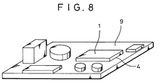
- the circuit board 9 to which the present invention can be applied includes, for example, a plastic film of polyimide, polyester, etc., a composite material such as a glass fiber-epoxy composite material, a semiconductor of silicon etc., and an inorganic substrate of glass, ceramic, etc.
- thermoplastic materials and various other materials which set on receiving heat or light can be used.
- those materials which set on receiving heat or light are used since they exhibit excellent heat resistance and humidity resistance after the connection.
- an epoxy adhesive containing a latent hardener and an acrylic adhesive containing a radical hardener such as peroxide are especially preferred because they set in a short period of time, can improve the efficiency of the connection work, and have excellent adhesive properties due to their molecular structure.
- the latent hardener has a relatively distinct activation point at which heat- or pressure-induced reaction starts, and thus is suited for the present invention involving the heat/pressure application step.
- imidazole As the latent hardener, imidazole, hydrazide, boron trifluoride-amine complex, amine-imide, polyamine salt, onium salt, dicyandiamide, and modified substances thereof may be used singly or in combination to form a mixture.
- catalytic hardeners of ionic polymerization type such as anionic or cationic polymerization type
- an imidazole hardener is especially preferred since it is non-metallic and thus is less susceptible to electrolytic corrosion and also in view of reactivity and connection reliability.
- other hardeners such as a polyamine hardener, a polymercaptan hardener, a polyphenol hardener and an acid anhydride hardener can be used, and also these hardeners may be used in combination with the aforementioned catalytic hardeners.
- a micro-encapsulated hardener in which the hardener as a core material is covered with a polymeric substance or an inorganic substance is also preferred because of its opposing properties, that is, long-term shelf stability and rapid setting property.
- the hardener for the adhesive used in the present invention should preferably have an activation temperature of 40 to 200°C. If the activation temperature is lower than 40°C, the difference between the activation temperature and room temperature is so small that the adhesive needs to be kept at low temperature, and if the activation temperature is higher than 200°C, other chips and the like are adversely affected by heat during the connection. For this reason, the activation temperature should preferably fall within a range of 50 to 150°C.
- the activation temperature mentioned herein represents an exothermic peak temperature of a compound of epoxy resin and the hardener, as a sample, which is measured by using a DSC (differential scanning calorimeter) while the sample is heated from room temperature at a rate of 10°C/min.
- the shelf stability of adhesive-coated chips is improved by carrying out heat treatment at a temperature lower than or equal to the activation temperature of the hardener, and excellent multi-chip connection is achieved at a temperature higher than or equal to the activation temperature.
- the melt viscosity of the adhesive is adjusted such that the aforementioned cohesion reduction line is formed at a temperature lower than or equal to the activation temperature of the hardener.
- the adhesive layer 4 is preferably admixed with electrically conducting particles 14 or with a small quantity of insulating particles (not shown), since the particles serve to maintain the layer thickness at the time of application of heat and pressure during the fabrication of adhesive-coated chips.
- the proportion of the conducting or insulating particles admixed in this case is approximately 0.1 to 30 vol %, and is set to 0.5 to 15 vol % in order to obtain anisotropic conductivity.
- the adhesive layer 4 may alternatively have a multilayer structure including an insulating layer and an electrically conducting layer formed separately from each other. In this case, resolution improves, permitting high-density connection of electrodes.
- the electrically conducting particles 14 may be metal particles of Au, Ag, Pt, Co, Ni, Cu, W, Sb, Sn or solder, or particles of carbon, graphite, etc. Further, such conducting particles or nonconductive particles, such as glass particles, ceramic particles or polymeric particles of plastic, may be used as cores, which are then coated with an electrically conductive layer using one of the above substances. Also, insulator-coated particles having electrically conducting cores coated with an insulating layer, or the combination of conducting particles and insulating particles of glass, ceramic or plastic may be used to improve the resolution.
- the particle size of the conducting particles 14 should preferably be as small as 15 ⁇ m or less, more preferably, in the range of 7 to 1 ⁇ m. If the particle size is smaller than 1 ⁇ m, difficulty arises in making the particles in contact with the electrode surfaces. Also, the conducting particles 14 should preferably be uniform in particle size, because uniform particle size serves to lessen the outflow of conducting particles from between electrodes facing each other.
- particles having polymeric cores of plastic material coated with a conductive layer and particles of heat-fusible metal such as solder are preferably used, because these particles deform when applied with pressure or both heat and pressure, so that the area of contact with circuits increases, thus improving the reliability.
- the particles do not show such a distinct melting point as that of solder, and thus the softened state can advantageously be controlled over a wide range of connection temperature and variations in the thickness or flatness of electrodes can be easily coped with.
- the conducting particles stick into the electrodes or wiring patterns, and thus low connection resistance is achieved even if an oxide film or a contamination layer exists on the electrode surface, whereby the reliability can be improved.
- the number of tapes with different widths may be small and the mounting apparatus can be simplified, as compared with the case of using different adhesive tapes for different sizes of chips. Further, unlike the case where an adhesive layer is formed over the entire surface of a circuit board, neither adjacent chips nor surrounding adhesive is adversely affected by heat or pressure, and no extra adhesive is used, which is advantageous from the economical viewpoint.
- the adhesive contains a latent hardener, and heat treatment is performed at a temperature lower than or equal to the activation temperature of the hardener to obtain adhesive-coated chips. Accordingly, the shelf stability of the adhesive is improved, and reliable multi-chip connection can be achieved at a temperature higher than or equal to the activation temperature.
- the pressure within the airtight vessel is kept constant, and a large number of MCM can be treated at the same time, whereby the mass production efficiency is enhanced. Also, since the heat treatment is carried out using gas or liquid as the medium, it is unnecessary to use expensive molds, and various adhesives having different properties in respect of heat, humidity and anaerobic characteristic can be used depending on the type of medium used. Further, even if the adhesive takes a long time to set, it is possible to produce a large number of MCM by one operation.
- the multi-chip mounting method of the present invention continuity test can be performed before the adhesive finally sets. Therefore, when defective connection is discovered, the adhesive is then still not sufficiently set, and thus the peeling of chips and the subsequent cleaning operation using a solvent such as acetone can be carried out very easily, thereby facilitating the repair work.
- a cohesion reduction line is readily formed in the adhesive layer around the chip when the chip is heated, and since the adhesive layer can be peeled from the separator, a chip coated with an adhesive layer having a size corresponding to the chip size can be obtained relatively easily.
- the heating temperature at a temperature lower than or equal to the activation temperature of the hardener, the adhesive-coated chips can be kept for later use without lowering their shelf stability.
- the adhesive layer is cut for at least part of its depth in the thickness direction by using a very simple cutting jig matching the chip shape, so that a chip coated with an adhesive layer having a size corresponding to the chip size can be obtained relatively easily.
- a solution containing 30% of ethyl acetate was obtained by mixing, in the ratio of 30/70, a phenoxy resin (polymeric epoxy resin) and a liquid epoxy resin (epoxy equivalent: 185) containing a micro-encapsulated latent hardener.
- a phenoxy resin polymeric epoxy resin
- a liquid epoxy resin epoxy equivalent: 185
- 2 vol % of electrically conducting particles which were obtained by coating polystyrene particles having a particle size of 3 ⁇ 0.2 ⁇ m with Ni and Au in thicknesses of 0.2 ⁇ m and 0.02 ⁇ m, respectively, followed by mixing and dispersion of the conducting particles.
- the dispersion was applied to a separator (polyethylene terephthalate film treated with silicone; thickness: 40 ⁇ m) by means of a roll coater, and the separator applied with the dispersion was dried at 100°C for 20 minutes to obtain an adhesive film with a thickness of 20 ⁇ m.
- a separator polyethylene terephthalate film treated with silicone; thickness: 40 ⁇ m
- the activation temperature of the adhesive film was measured using a DSC and was found to be 120°C.
- the viscosity of the adhesive layer was measured by a digital viscometer HV-8 (manufactured by Kabushiki Kaisha Reska), and was 800 poises at 100°C.
- the adhesive film was cut together with the separator to obtain a tape of 2 mm wide.
- the tape obtained in the manner described in (1) above was set in a chip mounting apparatus AC-SC450B (COB connecting apparatus manufactured by Hitachi Chemical Co., Ltd.) with its adhesive layer facing upward, and was held tense by rolls arranged in front and at the rear of the surface plate in such a manner that the tape could travel in close contact with the surface plate.
- An IC chip for evaluation (2 ⁇ 10 mm silicon substrate having a thickness of 0.5 mm and having 300 gold electrodes (called bumps) of 50 ⁇ m in diameter and 20 ⁇ m high formed near the two longer sides of the substrate) was fixed to the heating head in position by suction.
- the tape was subjected to heat-pressure bonding such that its adhesive layer was applied with 5 kg/cm 2 for 3 seconds, and then the heating head was raised to release the tape from pressure and separated from the surface plate.
- the actual temperature of the adhesive of the tape in contact with the surface of the IC chip was in this case 102°C at the maximum. In this manner, an adhesive-coated chip with an adhesive layer, which had been separated from the separator and had a size nearly identical to the chip size, was obtained.
- Two 5 ⁇ 5 mm IC chips (tape width: 5.5 mm) and one IC chip of 10 mm in diameter (tape width: 10.5 mm) were prepared in a like manner, thereby obtaining a total of four adhesive-coated chips. These chips had different bump pitches, but had the same bump height and the same silicon substrate thickness.
- the electrodes of the individual chips could be satisfactorily connected to the corresponding electrodes on the substrate. Since the adhesive was present only in the vicinity of the chips, almost no superfluous adhesive could be observed on the surface of the substrate. Further, one MCM could be obtained within one minute.
- IC chips were mounted on a substrate in substantially the same manner as in Example 1, but the adhesive-coated chips were produced by a different method. Specifically, a pressure head provided with a cutting jig was used, and the tape used had a width of 10 mm. For the 2 ⁇ 10 mm chip, for example, a heater wire comprising a nichrome wire and arranged so as to extend along the four sides of the chip was used as the cutting jig. The pressure head was not heated and was used at room temperature. Since a heater wire was used as the cutting jig, the tape could be cut for the entire depth inclusive of the separator, so that an adhesive-coated chip having a separator affixed to its adhesive layer was obtained.
- chips could also be similarly affixed with adhesive.
- a looped heater wire with an inner diameter of 11 mm was used as the cutting jig.
- the electrodes of the individual chips could be satisfactorily connected to the corresponding electrodes on the substrate. Since the adhesive was present only in the vicinity of the chips, almost no superfluous adhesive could be observed on the surface of the substrate.
- IC chips were mounted on a substrate in substantially the same manner as in Example 2, but when producing adhesive-coated chips, the temperature of the heating head was set at 70°C. Further, a cutting tool with a straight edge was used as the razor. Also in this case, adhesive-coated chips could be easily obtained. Since both the razor and the heating means were used, the adhesive could be readily transferred to the chips. Furthermore, the heating temperature could be set at a low temperature, as compared with the case of Example 1.
- IC chips were mounted on a substrate in substantially the same manner as in Example 1, but the adhesive-coated chips were producing by a different method. Specifically, various chips were temporarily fixed (by heat-pressure bonding at 100°C under 5 kg/cm 2 for 3 seconds) beforehand on a tape (width: 10.5 mm) so that the chips could be continuously fed in order, as shown in FIG. 7A, and adhesive-coated chips each with an adhesive layer, which had been separated from the separator and had a size nearly identical to the corresponding chip size, were obtained in the same manner as in Example 1. In this case, the adhesive could be easily peeled from the separator, and since the chips were prepared in order of mounting, the productivity was extremely high. The electrodes of the individual chips could be satisfactorily connected to the corresponding electrodes on the substrate.
- Adhesive-coated chips obtained in the same manner as in Example 4 were again temporarily fixed on a continuous separator at intervals of 1 mm between adjacent chips, to obtain a series of adhesive-coated chips as shown in FIG. 7B.
- the productivity was extremely high because the chips could be removed from the separator in mounting order.
- the electrodes of the individual chips could be satisfactorily connected to the corresponding electrodes on the substrate.
- the series of adhesive-coated chips could be wound on a reel with an outside diameter of 55 mm into a compact size, the chips could be easily kept in cold storage after operation.
- the electrodes of the individual chips could be satisfactorily connected to the corresponding electrodes on the substrate.
- IC chips were mounted on a substrate in substantially the same manner as in Example 1, but a different adhesive was used. Specifically, when preparing the adhesive mentioned above, no electrically conducting particles were added. Also in this case, the electrodes of the individual chips could be satisfactorily connected to the corresponding electrodes on the substrate. Presumably this is because the bumps of the chips and the connection electrodes of the glass epoxy substrate were brought into direct contact with each other and were firmly bonded together by the adhesive.
- IC chips were mounted on a substrate in substantially the same manner as in Example 1, but an intermediate inspection step was additionally provided to inspect the electrical connection between the electrodes after the adhesive-coated chips were obtained.
- the adhesive-coated chips using the adhesive obtained according to Example 6 were heated at 150°C under 20 kgf/mm 2 , and upon lapse of 2 seconds, the connection resistance at individual connection points was measured using a multimeter while the chips were kept under pressure. Similar adhesive-coated chips were connected at 150°C under 20 kgf/mm 2 for 4 seconds, and then removed the substrate from the connecting apparatus. Since in this stage the adhesive had started to set due to application of heat and pressure, the individual IC chips were temporarily fixed on the substrates. These substrates were inspected with no pressure applied thereto, and had one defective IC chip each.
- the defective IC chips were mechanically peeled off and new chips were connected in the aforementioned manner; in this case, the chips could be satisfactorily connected.
- the adhesives were not sufficiently set, the peeling of the chips and the subsequent cleaning operation using a solvent could be performed very easily, facilitating the repair work.
- the rates of reaction of the adhesives were measured in terms of heat quantity, and were found to be 7% in the former case and 20% in the latter.
- the IC chips were connected at 150°C under 20 kgf/mm 2 for 15 seconds, and they showed good connection characteristics in both cases. After the adhesive sets, it is extremely difficult to peel off the chips and clean the substrate by using a solvent, but according to this example, repair work could be performed with ease though numerous chips were mounted on a small-sized substrate.
- IC chips were mounted on a substrate by a method similar to that employed in Example 1, but static pressure was utilized in the step of applying heat and pressure at the time of connection.
- adhesive-coated chips were placed on a glass epoxy substrate, and after the electrodes were positioned relative to each other using a CCD camera, the substrate having the chips temporarily fixed thereon was set in a pressure pot for pneumatic pressure treatment at 120°C under 20 kg/cm 2 for 30 minutes, then cooled to room temperature, and removed from the pressure pot.
- a pressure pot for pneumatic pressure treatment at 120°C under 20 kg/cm 2 for 30 minutes, then cooled to room temperature, and removed from the pressure pot.
- the individual chips can be applied with uniform pressure regardless of their heights, it is unnecessary to use a buffering member unlike Example 1. Also, it is possible to treat a large number of MCM at a time depending on the capacity of the pressure pot.
- IC chips were mounted on a substrate in substantially the same manner as in Example 1, but a polytetrafluoroethylene film (thickness: 80 ⁇ m) was used as the separator.
- the obtained MCM was evaluated in the same manner as in Example 1, and it was found that the adhesive could be transferred to the surfaces of the chips in more exact shape matching the chip size especially at the edges. Presumably this is because the separator was more flexible than that used in Example 1 and thus the adhesive could be cut sharply along the edges of the chips.
- the elasticity modulus of the polyethylene terephthalate film was 200 kgf/mm 2
- the elasticity modulus of the polytetrafluoroethylene film was 40 kgf/mm 2 .
- IC chips were mounted on a substrate in substantially the same manner as in Example 1, but the adhesive-coated chips were produced with a silicone rubber sheet of 0.5 mm thick interposed between the separator and the surface plate.
- the adhesive could be transferred to the surfaces of the chips in more exact shape matching the chip size than in Example 1, especially at the edges. This is presumably because the silicone rubber sheet served as a cushioning member.
- the thickness of the adhesive layer formed on the electrode surface is controlled by the heights of the bumps and the electrically conducting particles; therefore, the bumps each had an adhesive layer of about 4 ⁇ m thick formed thereon and the region other than the bumps had an adhesive layer of about 20 ⁇ m thick formed thereon, which thickness is identical to the original thickness.
- Example 1 Following the method of mounting IC chips on a substrate employed in Example 1, the adhesive film with the separator was cut into pieces corresponding in shape to respective chip sizes, and the cut pieces were affixed to the respective electrode surfaces. Since the chips were small, it took much time to affix the cut pieces accurately to the chips. More than twenty minutes were required to obtain one MCM, and thus the efficiency was low compared with Example 1 in which one MCM could be produced within one minute.
- the adhesive layer can be formed accurately on the electrode surfaces of individual chips with different sizes, and also multiple chips of different sizes can be mounted at a time, whereby MCM can be fabricated with high efficiency.
Landscapes
- Engineering & Computer Science (AREA)
- Manufacturing & Machinery (AREA)
- Microelectronics & Electronic Packaging (AREA)
- Wire Bonding (AREA)
- Electric Connection Of Electric Components To Printed Circuits (AREA)
- Die Bonding (AREA)
- Adhesive Tapes (AREA)
Applications Claiming Priority (3)
| Application Number | Priority Date | Filing Date | Title |
|---|---|---|---|
| JP20687496 | 1996-08-06 | ||
| JP206874/96 | 1996-08-06 | ||
| JP20687496 | 1996-08-06 |
Publications (3)
| Publication Number | Publication Date |
|---|---|
| EP0824270A2 true EP0824270A2 (fr) | 1998-02-18 |
| EP0824270A3 EP0824270A3 (fr) | 1999-06-09 |
| EP0824270B1 EP0824270B1 (fr) | 2004-01-02 |
Family
ID=16530482
Family Applications (1)
| Application Number | Title | Priority Date | Filing Date |
|---|---|---|---|
| EP97113530A Expired - Lifetime EP0824270B1 (fr) | 1996-08-06 | 1997-08-06 | Procédé pour le montage d'une pluralité de pièces électroniques sur un panneau de circuit |
Country Status (7)
| Country | Link |
|---|---|
| US (3) | US6158115A (fr) |
| EP (1) | EP0824270B1 (fr) |
| JP (3) | JP3928753B2 (fr) |
| KR (1) | KR100278594B1 (fr) |
| CN (1) | CN1098617C (fr) |
| DE (1) | DE69727014T2 (fr) |
| TW (1) | TW428259B (fr) |
Cited By (12)
| Publication number | Priority date | Publication date | Assignee | Title |
|---|---|---|---|---|
| EP1085790A1 (fr) * | 1999-09-17 | 2001-03-21 | Sony Chemicals Corporation | Matériel de connexion |
| WO2002041387A1 (fr) * | 2000-11-20 | 2002-05-23 | Rafsec Oy | Procede pour fixer un circuit integre sur une puce de silicium a une etiquette intelligente |
| US6462284B1 (en) | 1998-07-01 | 2002-10-08 | Seiko Epson Corporation | Semiconductor device and method of manufacture thereof |
| FR2824185A1 (fr) * | 2001-04-25 | 2002-10-31 | Gemplus Card Int | Report direct ou indirect d'adhesif anisotropique de report de puces sur une plaquette |
| EP1160857A3 (fr) * | 2000-06-01 | 2004-01-02 | Sony Chemicals Corp. | Colle à base de résine époxyde pour le montage d'un composant semi-conducteur sur un substrat |
| EP1454973A1 (fr) * | 1998-08-13 | 2004-09-08 | Hitachi Chemical Co., Ltd. | Adhésif pour fixer des éléments de circuit, cartre de circuit imprimé et procédé de production |
| US6951621B2 (en) | 2000-03-31 | 2005-10-04 | Rafsec Oy | Method for forming a product sensor, and a product sensor |
| EP1599078A3 (fr) * | 2004-04-22 | 2006-10-11 | Semikron Elektronik GmbH & Co. KG Patentabteilung | Méthode de montage d'un composant électrique sur un substrat |
| US7244332B2 (en) | 2000-12-11 | 2007-07-17 | Rafsec Oy | Smart label web and a method for its manufacture |
| US7247381B1 (en) | 1998-08-13 | 2007-07-24 | Hitachi Chemical Company, Ltd. | Adhesive for bonding circuit members, circuit board, and method of producing the same |
| US9044898B2 (en) | 2012-04-03 | 2015-06-02 | Apple Inc. | Methods for joining electronic device housing structures using heat activated thermoset film |
| CN108604555A (zh) * | 2015-10-08 | 2018-09-28 | 贺利氏德国有限两合公司 | 用预固剂涂覆接触材料层以将衬底布置连接到电子组件的方法、相应的衬底布置及其制造方法 |
Families Citing this family (57)
| Publication number | Priority date | Publication date | Assignee | Title |
|---|---|---|---|---|
| US6534724B1 (en) * | 1997-05-28 | 2003-03-18 | International Business Machines Corporation | Enhanced design and process for a conductive adhesive |
| US6541872B1 (en) | 1999-01-11 | 2003-04-01 | Micron Technology, Inc. | Multi-layered adhesive for attaching a semiconductor die to a substrate |
| JP3543676B2 (ja) | 1999-06-02 | 2004-07-14 | セイコーエプソン株式会社 | マルチチップの実装構造及びその実装構造の製造方法、ならびに電気光学装置及び電子機器 |
| USRE45402E1 (en) | 1999-07-13 | 2015-03-03 | Stirling Mouldings Limited | Flexible material |
| GB2352208B (en) | 1999-07-13 | 2001-06-13 | Stirling Moulded Composites Lt | Flexible material |
| SG99331A1 (en) * | 2000-01-13 | 2003-10-27 | Hitachi Ltd | Method of producing electronic part with bumps and method of producing elctronic part |
| JP2001323246A (ja) * | 2000-03-07 | 2001-11-22 | Sony Chem Corp | 電極接続用接着剤及びこれを用いた接着方法 |
| JP2002033296A (ja) * | 2000-04-26 | 2002-01-31 | Lintec Corp | シリコンウエハ用の補強材および該補強材を用いたicチップの製造方法 |
| TW543052B (en) * | 2001-03-05 | 2003-07-21 | Nitto Denko Corp | Manufacturing method of ceramic green sheet, manufacturing method of multilayer ceramic electronic components, and carrier sheet for ceramic green sheets |
| FI112550B (fi) | 2001-05-31 | 2003-12-15 | Rafsec Oy | Älytarra ja älytarraraina |
| FI117331B (fi) | 2001-07-04 | 2006-09-15 | Rafsec Oy | Menetelmä ruiskuvaletun tuotteen valmistamiseksi |
| US6871395B2 (en) * | 2001-08-06 | 2005-03-29 | Siemens Technology-To-Business Center, Llc. | Methods for manufacturing a tactile sensor using an electrically conductive elastomer |
| JP4710205B2 (ja) * | 2001-09-06 | 2011-06-29 | ソニー株式会社 | フリップチップ実装方法 |
| KR20040052126A (ko) * | 2002-12-13 | 2004-06-19 | 엘지전선 주식회사 | 이방 도전성 접착제, 이를 이용한 회로 접속 방법 및 회로접속 구조체 |
| FI115601B (fi) * | 2003-04-01 | 2005-05-31 | Imbera Electronics Oy | Menetelmä elektroniikkamoduulin valmistamiseksi ja elektroniikkamoduuli |
| JP4627654B2 (ja) * | 2004-12-09 | 2011-02-09 | 芝浦メカトロニクス株式会社 | 部品の組み立て装置及び組み立て方法 |
| JP2006199756A (ja) * | 2005-01-18 | 2006-08-03 | Sekisui Chem Co Ltd | 接合フィルム、電子部品装置の製造方法及び電子部品装置 |
| US7888604B2 (en) * | 2005-04-11 | 2011-02-15 | 3M Innovative Properties Company | Connection method of a flexible printed circuit board with two printed circuit boards, and electric or electronic component with parts connected by the connection method |
| DE102005041354B3 (de) * | 2005-08-31 | 2007-01-25 | Siemens Audiologische Technik Gmbh | Verfahren zum Bestücken einer Leiterplatine durch isostatische Kräfte |
| US20070246839A1 (en) * | 2006-04-21 | 2007-10-25 | Applied Materials, Inc. | Method of proximity pin manufacture |
| US20100021667A1 (en) * | 2006-04-24 | 2010-01-28 | Hitachi Chemical Company, Ltd. | Adhesive tape |
| MY153208A (en) * | 2006-09-15 | 2015-01-29 | Lintec Corp | Process for manufacturing semiconductor devices |
| TWI326484B (en) * | 2006-09-21 | 2010-06-21 | Advanced Chip Eng Tech Inc | Chip package and chip package array |
| JP5100081B2 (ja) * | 2006-10-20 | 2012-12-19 | 新光電気工業株式会社 | 電子部品搭載多層配線基板及びその製造方法 |
| US20080113143A1 (en) * | 2006-10-31 | 2008-05-15 | David Stirling Taylor | Flexible Material and Method of Manufacturing the Flexible Material |
| DE102007019570A1 (de) * | 2007-04-25 | 2008-10-30 | Carl Zeiss Smt Ag | Spiegelanordnung, Kontaktierungsanordnung und optisches System |
| JP2008085354A (ja) * | 2007-10-22 | 2008-04-10 | Toshiba Corp | 半導体製造装置 |
| KR101290728B1 (ko) * | 2008-03-07 | 2013-07-26 | 삼성전자주식회사 | 전극 모듈 및 이를 이용한 탈이온화 장치 |
| JP4998360B2 (ja) * | 2008-04-16 | 2012-08-15 | パナソニック株式会社 | 電子部品モジュールの製造方法 |
| JP4596034B2 (ja) * | 2008-04-16 | 2010-12-08 | パナソニック株式会社 | 電子部品モジュールの製造方法 |
| US10499694B2 (en) | 2008-08-01 | 2019-12-10 | Nike, Inc. | Apparel with selectively attachable and detachable elements |
| US20100024089A1 (en) | 2008-08-01 | 2010-02-04 | Nike, Inc. | Apparel With Selectively Attachable And Detachable Elements |
| JP5224111B2 (ja) * | 2008-08-29 | 2013-07-03 | 日立化成株式会社 | 半導体ウェハ加工用接着フィルム |
| JP4360446B1 (ja) * | 2008-10-16 | 2009-11-11 | 住友ベークライト株式会社 | 半導体装置の製造方法及び半導体装置 |
| JP2009188414A (ja) * | 2009-03-30 | 2009-08-20 | Hitachi Chem Co Ltd | 接着剤テープの圧着方法 |
| US9675122B2 (en) | 2009-06-23 | 2017-06-13 | Nike, Inc. | Apparel incorporating a protective element |
| US9149084B2 (en) | 2009-06-23 | 2015-10-06 | Nike, Inc. | Apparel incorporating a protective element and method for making |
| US8438669B2 (en) | 2009-06-23 | 2013-05-14 | Nike, Inc. | Apparel incorporating a protective element |
| US8438667B2 (en) | 2009-09-24 | 2013-05-14 | Nike, Inc. | Apparel incorporating a protective element |
| US8719965B2 (en) | 2009-09-24 | 2014-05-13 | Nike, Inc. | Apparel incorporating a protective element |
| JP5249184B2 (ja) * | 2009-12-09 | 2013-07-31 | 株式会社日立ハイテクノロジーズ | フラットパネルディスプレイの実装装置および実装方法 |
| US8702895B2 (en) | 2010-04-07 | 2014-04-22 | Nike, Inc. | Cushioning elements for apparel and other products and methods of manufacturing the cushioning elements |
| US9505203B2 (en) | 2010-11-30 | 2016-11-29 | Nike, Inc. | Method of manufacturing dye-sublimation printed elements |
| US8561214B2 (en) | 2011-02-25 | 2013-10-22 | Nike, Inc. | Articles of apparel incorporating cushioning elements and methods of manufacturing the articles of apparel |
| US8764931B2 (en) | 2011-05-19 | 2014-07-01 | Nike, Inc. | Method of manufacturing cushioning elements for apparel and other products |
| US10034498B2 (en) | 2011-07-25 | 2018-07-31 | Nike, Inc. | Articles of apparel incorporating cushioning elements |
| US20130025036A1 (en) | 2011-07-25 | 2013-01-31 | Nike, Inc. | Articles Of Apparel Incorporating Cushioning Elements |
| US9386812B2 (en) | 2011-07-25 | 2016-07-12 | Nike, Inc. | Articles of apparel incorporating cushioning elements |
| JP6002135B2 (ja) * | 2011-08-05 | 2016-10-05 | パナソニック株式会社 | フレキシブルデバイスの製造方法 |
| JP2013122957A (ja) * | 2011-12-09 | 2013-06-20 | Dexerials Corp | 接続方法、接続構造体、絶縁性接着部材、及び、接着部材付電子部品及びその製造方法 |
| WO2014203603A1 (fr) * | 2013-06-18 | 2014-12-24 | 株式会社村田製作所 | Procédé pour fabriquer un substrat en résine à couches multiples |
| US9673170B2 (en) | 2014-08-05 | 2017-06-06 | Infineon Technologies Ag | Batch process for connecting chips to a carrier |
| WO2022236750A1 (fr) * | 2021-05-12 | 2022-11-17 | 重庆康佳光电技术研究院有限公司 | Composant provisoire de puce, panneau d'affichage et procédé de fabrication associé |
| CN115347085A (zh) * | 2021-05-12 | 2022-11-15 | 重庆康佳光电技术研究院有限公司 | 芯片临时组件、显示面板及其制作方法 |
| CN113873780B (zh) * | 2021-10-19 | 2024-01-26 | 西安微电子技术研究所 | 一种径向片式电容的粘固方法 |
| JP2025098296A (ja) * | 2022-03-31 | 2025-07-02 | リンテック株式会社 | 積層体の製造方法 |
| CN115942662B (zh) * | 2022-06-29 | 2025-06-24 | 北京小米移动软件有限公司 | 电子设备的壳体结构和镜片安装方法及其参数确定方法 |
Family Cites Families (37)
| Publication number | Priority date | Publication date | Assignee | Title |
|---|---|---|---|---|
| US622839A (en) * | 1899-04-11 | Acetylene-gas generator | ||
| US3639188A (en) * | 1970-05-21 | 1972-02-01 | Ibm | Method of manufacture of a magnetic disk and recording surface |
| US3724068A (en) * | 1971-02-25 | 1973-04-03 | Du Pont | Semiconductor chip packaging apparatus and method |
| US5158818A (en) * | 1984-01-30 | 1992-10-27 | National Starch And Chemical Investment Holding Corporation | Conductive die attach tape |
| US4959008A (en) * | 1984-04-30 | 1990-09-25 | National Starch And Chemical Investment Holding Corporation | Pre-patterned circuit board device-attach adhesive transfer system |
| US4554033A (en) * | 1984-10-04 | 1985-11-19 | Amp Incorporated | Method of forming an electrical interconnection means |
| IN168174B (fr) * | 1986-04-22 | 1991-02-16 | Siemens Ag | |
| EP0265077A3 (fr) * | 1986-09-25 | 1989-03-08 | Sheldahl, Inc. | Une colle anisotropique pour lier des composants électriques |
| CA1290676C (fr) * | 1987-03-30 | 1991-10-15 | William Frank Graham | Methode de soudage de puces de circuits integres |
| US4917466A (en) * | 1987-08-13 | 1990-04-17 | Shin-Etsu Polymer Co., Ltd. | Method for electrically connecting IC chips, a resinous bump-forming composition used therein and a liquid-crystal display unit electrically connected thereby |
| JPH01299884A (ja) * | 1988-05-28 | 1989-12-04 | Tomoegawa Paper Co Ltd | ダイボンディング接着テープ |
| US5277972B1 (en) * | 1988-09-29 | 1996-11-05 | Tomoegawa Paper Co Ltd | Adhesive tapes |
| US5077633A (en) * | 1989-05-01 | 1991-12-31 | Motorola Inc. | Grounding an ultra high density pad array chip carrier |
| JP2974700B2 (ja) * | 1989-11-30 | 1999-11-10 | 東レ・ダウコーニング・シリコーン株式会社 | 導電性接着剤 |
| US5074947A (en) | 1989-12-18 | 1991-12-24 | Epoxy Technology, Inc. | Flip chip technology using electrically conductive polymers and dielectrics |
| US5611140A (en) * | 1989-12-18 | 1997-03-18 | Epoxy Technology, Inc. | Method of forming electrically conductive polymer interconnects on electrical substrates |
| JPH0777136B2 (ja) * | 1990-10-31 | 1995-08-16 | 信越ポリマー株式会社 | 加熱硬化型異方導電接続部材 |
| JPH04246839A (ja) * | 1991-02-01 | 1992-09-02 | Matsushita Electric Ind Co Ltd | Ic実装方法 |
| JP2682250B2 (ja) * | 1991-03-20 | 1997-11-26 | 株式会社村田製作所 | 電子部品チップ用ホルダおよび電子部品チップの取扱方法 |
| JPH04303582A (ja) * | 1991-03-30 | 1992-10-27 | Nec Corp | 圧着方法および圧着装置 |
| JP3163751B2 (ja) * | 1992-06-11 | 2001-05-08 | 松下電器産業株式会社 | 半導体装置の製造方法 |
| US5436503A (en) * | 1992-11-18 | 1995-07-25 | Matsushita Electronics Corporation | Semiconductor device and method of manufacturing the same |
| US5667884A (en) * | 1993-04-12 | 1997-09-16 | Bolger; Justin C. | Area bonding conductive adhesive preforms |
| IT1261464B (it) * | 1993-04-30 | 1996-05-23 | Consorzio Eagle | Procedimento per la connessione di un circuito integrato ad un circuito esterno. |
| US5616206A (en) * | 1993-06-15 | 1997-04-01 | Ricoh Company, Ltd. | Method for arranging conductive particles on electrodes of substrate |
| JPH0730236A (ja) * | 1993-07-08 | 1995-01-31 | Hitachi Ltd | 部品の搭載方法 |
| JP2985640B2 (ja) * | 1994-02-10 | 1999-12-06 | 松下電器産業株式会社 | 電極接続体及びその製造方法 |
| JPH07240435A (ja) * | 1994-03-02 | 1995-09-12 | Toshiba Corp | 半導体パッケージの製造方法、半導体の実装方法、および半導体実装装置 |
| TW277152B (fr) * | 1994-05-10 | 1996-06-01 | Hitachi Chemical Co Ltd | |
| US5652055A (en) * | 1994-07-20 | 1997-07-29 | W. L. Gore & Associates, Inc. | Matched low dielectric constant, dimensionally stable adhesive sheet |
| JPH0837208A (ja) * | 1994-07-25 | 1996-02-06 | Toshiba Corp | 半導体素子の実装方法およびその装置 |
| KR0181615B1 (ko) * | 1995-01-30 | 1999-04-15 | 모리시다 요이치 | 반도체 장치의 실장체, 그 실장방법 및 실장용 밀봉재 |
| US5736074A (en) * | 1995-06-30 | 1998-04-07 | Micro Fab Technologies, Inc. | Manufacture of coated spheres |
| CN1194059A (zh) * | 1995-08-29 | 1998-09-23 | 美国3M公司 | 用于粘合电子器件的可变形基片部件 |
| JPH09219578A (ja) * | 1996-02-13 | 1997-08-19 | Oki Electric Ind Co Ltd | 電子部品の接続方法及び接続装置 |
| US6034331A (en) * | 1996-07-23 | 2000-03-07 | Hitachi Chemical Company, Ltd. | Connection sheet and electrode connection structure for electrically interconnecting electrodes facing each other, and method using the connection sheet |
| US5972152A (en) | 1997-05-16 | 1999-10-26 | Micron Communications, Inc. | Methods of fixturing flexible circuit substrates and a processing carrier, processing a flexible circuit and processing a flexible circuit substrate relative to a processing carrier |
-
1997
- 1997-07-22 JP JP19568797A patent/JP3928753B2/ja not_active Expired - Lifetime
- 1997-08-02 TW TW086111049A patent/TW428259B/zh not_active IP Right Cessation
- 1997-08-06 KR KR19970037541A patent/KR100278594B1/ko not_active Expired - Fee Related
- 1997-08-06 US US08/907,017 patent/US6158115A/en not_active Expired - Lifetime
- 1997-08-06 CN CN97117465A patent/CN1098617C/zh not_active Expired - Fee Related
- 1997-08-06 EP EP97113530A patent/EP0824270B1/fr not_active Expired - Lifetime
- 1997-08-06 DE DE69727014T patent/DE69727014T2/de not_active Expired - Lifetime
-
2000
- 2000-10-12 US US09/685,951 patent/US6479757B1/en not_active Expired - Fee Related
-
2002
- 2002-10-01 US US10/260,342 patent/US6841022B2/en not_active Expired - Fee Related
-
2009
- 2009-07-21 JP JP2009170295A patent/JP2009283962A/ja active Pending
- 2009-07-21 JP JP2009170291A patent/JP2009283961A/ja active Pending
Cited By (23)
| Publication number | Priority date | Publication date | Assignee | Title |
|---|---|---|---|---|
| US8273458B2 (en) | 1997-02-14 | 2012-09-25 | Hitachi Chemical Company, Ltd. | Adhesive for bonding circuit members, circuit board and process for its production |
| US7868466B2 (en) | 1998-07-01 | 2011-01-11 | Seiko Epson Corporation | Semiconductor device and method of manufacture thereof, circuit board and electronic instrument |
| US6763994B2 (en) | 1998-07-01 | 2004-07-20 | Nobuaki Hashimoto | Semiconductor device and method of manufacture thereof, circuit board and electronic instrument |
| US7332371B2 (en) | 1998-07-01 | 2008-02-19 | Seiko Epson Corporation | Semiconductor device and method of manufacture thereof, circuit board and electronic instrument |
| US6972381B2 (en) | 1998-07-01 | 2005-12-06 | Seiko Epson Corporation | Semiconductor device and method of manufacture thereof, circuit board and electronic instrument |
| US6462284B1 (en) | 1998-07-01 | 2002-10-08 | Seiko Epson Corporation | Semiconductor device and method of manufacture thereof |
| SG102032A1 (en) * | 1998-07-01 | 2004-02-27 | Seiko Epson Corp | Semiconductor device and method of its manufacture |
| US8252419B2 (en) | 1998-08-13 | 2012-08-28 | Hitachi Chemical Company, Ltd. | Adhesive for bonding circuit members, circuit board and process for its production |
| US8273457B2 (en) | 1998-08-13 | 2012-09-25 | Hitachi Chemical Company, Ltd. | Adhesive for bonding circuit members, circuit board and process for its production |
| US7247381B1 (en) | 1998-08-13 | 2007-07-24 | Hitachi Chemical Company, Ltd. | Adhesive for bonding circuit members, circuit board, and method of producing the same |
| EP1454973A1 (fr) * | 1998-08-13 | 2004-09-08 | Hitachi Chemical Co., Ltd. | Adhésif pour fixer des éléments de circuit, cartre de circuit imprimé et procédé de production |
| US7879445B2 (en) | 1998-08-13 | 2011-02-01 | Hitachi Chemical Company, Ltd. | Adhesive for bonding circuit members, circuit board and process for its production |
| US6566422B1 (en) | 1999-09-17 | 2003-05-20 | Sony Chemicals Corporation | Connecting material |
| EP1085790A1 (fr) * | 1999-09-17 | 2001-03-21 | Sony Chemicals Corporation | Matériel de connexion |
| US6951621B2 (en) | 2000-03-31 | 2005-10-04 | Rafsec Oy | Method for forming a product sensor, and a product sensor |
| EP1160857A3 (fr) * | 2000-06-01 | 2004-01-02 | Sony Chemicals Corp. | Colle à base de résine époxyde pour le montage d'un composant semi-conducteur sur un substrat |
| WO2002041387A1 (fr) * | 2000-11-20 | 2002-05-23 | Rafsec Oy | Procede pour fixer un circuit integre sur une puce de silicium a une etiquette intelligente |
| US7244332B2 (en) | 2000-12-11 | 2007-07-17 | Rafsec Oy | Smart label web and a method for its manufacture |
| FR2824185A1 (fr) * | 2001-04-25 | 2002-10-31 | Gemplus Card Int | Report direct ou indirect d'adhesif anisotropique de report de puces sur une plaquette |
| EP1599078A3 (fr) * | 2004-04-22 | 2006-10-11 | Semikron Elektronik GmbH & Co. KG Patentabteilung | Méthode de montage d'un composant électrique sur un substrat |
| US9044898B2 (en) | 2012-04-03 | 2015-06-02 | Apple Inc. | Methods for joining electronic device housing structures using heat activated thermoset film |
| CN108604555A (zh) * | 2015-10-08 | 2018-09-28 | 贺利氏德国有限两合公司 | 用预固剂涂覆接触材料层以将衬底布置连接到电子组件的方法、相应的衬底布置及其制造方法 |
| CN108604555B (zh) * | 2015-10-08 | 2022-03-08 | 贺利氏德国有限两合公司 | 用预固剂涂覆接触材料层以将衬底布置连接到电子组件的方法、相应的衬底布置及其制造方法 |
Also Published As
| Publication number | Publication date |
|---|---|
| US6158115A (en) | 2000-12-12 |
| DE69727014D1 (de) | 2004-02-05 |
| CN1174490A (zh) | 1998-02-25 |
| CN1098617C (zh) | 2003-01-08 |
| US6479757B1 (en) | 2002-11-12 |
| EP0824270A3 (fr) | 1999-06-09 |
| TW428259B (en) | 2001-04-01 |
| US20030029556A1 (en) | 2003-02-13 |
| DE69727014T2 (de) | 2004-06-09 |
| JPH10107048A (ja) | 1998-04-24 |
| EP0824270B1 (fr) | 2004-01-02 |
| US6841022B2 (en) | 2005-01-11 |
| JP2009283962A (ja) | 2009-12-03 |
| JP3928753B2 (ja) | 2007-06-13 |
| JP2009283961A (ja) | 2009-12-03 |
| KR100278594B1 (fr) | 2001-01-15 |
Similar Documents
| Publication | Publication Date | Title |
|---|---|---|
| US6158115A (en) | Method of mounting a plurality of electronic parts on a circuit board | |
| US6113728A (en) | Process for connecting circuits and adhesive film used therefor | |
| US6338195B1 (en) | Connection sheet and electrode connection structure for electrically interconnecting electrodes facing each other, and method using the connection sheet | |
| WO1999049507A1 (fr) | Technique de montage par bosses soudees | |
| JPH0334853B2 (fr) | ||
| EP0527387B1 (fr) | Procédés et dispositif pour fixer un plot de contact aux conducteurs d'une bande TAB | |
| EP0544305A2 (fr) | Procédé de fabrication d'un plot de contact utilisant un film composé | |
| JP3959654B2 (ja) | マルチチップ実装法 | |
| JP4574631B2 (ja) | マルチチップ実装法 | |
| JPH1050930A5 (fr) | ||
| Hatada et al. | New film carrier assembly technology: Transferred bump TAB | |
| KR100251674B1 (ko) | 서로 마주보는 전극들을 상호접속하기 위한 접속시트, 및이 접속시트를 사용하는 전극접속구조 및 접속방법 | |
| JP4223581B2 (ja) | マルチチップ実装法 | |
| JP4045471B2 (ja) | 電子部品実装法 | |
| JP4193885B2 (ja) | マルチチップ実装法 | |
| JP2002124527A (ja) | チップ状電子部品の製造方法、及びその製造に用いる疑似ウェーハの製造方法 | |
| JP2007184653A (ja) | マルチチップモジュールの実装方法 | |
| JP4197026B2 (ja) | マルチチップ実装方法 | |
| JPH1050927A (ja) | マルチチップ実装法 | |
| JP4337941B2 (ja) | マルチチップ実装方法 | |
| JP4254849B2 (ja) | マルチチップ実装法 | |
| JPH0462480B2 (fr) | ||
| JP3594502B2 (ja) | 半導体パッケージの製造方法及びその装置 | |
| TW202502991A (zh) | 含填料膜、接合體及其製造方法 | |
| JPH04301383A (ja) | 接続部材の製造方法 |
Legal Events
| Date | Code | Title | Description |
|---|---|---|---|
| PUAI | Public reference made under article 153(3) epc to a published international application that has entered the european phase |
Free format text: ORIGINAL CODE: 0009012 |
|
| AK | Designated contracting states |
Kind code of ref document: A2 Designated state(s): DE FR GB NL SE |
|
| AX | Request for extension of the european patent |
Free format text: AL;LT;LV;RO;SI |
|
| PUAL | Search report despatched |
Free format text: ORIGINAL CODE: 0009013 |
|
| AK | Designated contracting states |
Kind code of ref document: A3 Designated state(s): AT BE CH DE DK ES FI FR GB GR IE IT LI LU MC NL PT SE |
|
| AX | Request for extension of the european patent |
Free format text: AL;LT;LV;RO;SI |
|
| 17P | Request for examination filed |
Effective date: 19990630 |
|
| AKX | Designation fees paid |
Free format text: DE FR GB NL SE |
|
| 17Q | First examination report despatched |
Effective date: 20020606 |
|
| GRAP | Despatch of communication of intention to grant a patent |
Free format text: ORIGINAL CODE: EPIDOSNIGR1 |
|
| GRAS | Grant fee paid |
Free format text: ORIGINAL CODE: EPIDOSNIGR3 |
|
| GRAA | (expected) grant |
Free format text: ORIGINAL CODE: 0009210 |
|
| AK | Designated contracting states |
Kind code of ref document: B1 Designated state(s): DE FR GB NL SE |
|
| REG | Reference to a national code |
Ref country code: GB Ref legal event code: FG4D |
|
| REF | Corresponds to: |
Ref document number: 69727014 Country of ref document: DE Date of ref document: 20040205 Kind code of ref document: P |
|
| REG | Reference to a national code |
Ref country code: SE Ref legal event code: TRGR |
|
| ET | Fr: translation filed | ||
| PLBE | No opposition filed within time limit |
Free format text: ORIGINAL CODE: 0009261 |
|
| STAA | Information on the status of an ep patent application or granted ep patent |
Free format text: STATUS: NO OPPOSITION FILED WITHIN TIME LIMIT |
|
| 26N | No opposition filed |
Effective date: 20041005 |
|
| PGFP | Annual fee paid to national office [announced via postgrant information from national office to epo] |
Ref country code: FR Payment date: 20110818 Year of fee payment: 15 Ref country code: SE Payment date: 20110811 Year of fee payment: 15 |
|
| PGFP | Annual fee paid to national office [announced via postgrant information from national office to epo] |
Ref country code: GB Payment date: 20120821 Year of fee payment: 16 |
|
| REG | Reference to a national code |
Ref country code: DE Ref legal event code: R082 Ref document number: 69727014 Country of ref document: DE Representative=s name: VON ROHR PATENTANWAELTE PARTNERSCHAFT MBB, DE |
|
| PGFP | Annual fee paid to national office [announced via postgrant information from national office to epo] |
Ref country code: DE Payment date: 20120822 Year of fee payment: 16 |
|
| PGFP | Annual fee paid to national office [announced via postgrant information from national office to epo] |
Ref country code: NL Payment date: 20120821 Year of fee payment: 16 |
|
| REG | Reference to a national code |
Ref country code: SE Ref legal event code: EUG |
|
| PG25 | Lapsed in a contracting state [announced via postgrant information from national office to epo] |
Ref country code: SE Free format text: LAPSE BECAUSE OF NON-PAYMENT OF DUE FEES Effective date: 20120807 |
|
| REG | Reference to a national code |
Ref country code: FR Ref legal event code: ST Effective date: 20130430 |
|
| PG25 | Lapsed in a contracting state [announced via postgrant information from national office to epo] |
Ref country code: FR Free format text: LAPSE BECAUSE OF NON-PAYMENT OF DUE FEES Effective date: 20120831 |
|
| REG | Reference to a national code |
Ref country code: NL Ref legal event code: V1 Effective date: 20140301 |
|
| GBPC | Gb: european patent ceased through non-payment of renewal fee |
Effective date: 20130806 |
|
| PG25 | Lapsed in a contracting state [announced via postgrant information from national office to epo] |
Ref country code: NL Free format text: LAPSE BECAUSE OF NON-PAYMENT OF DUE FEES Effective date: 20140301 Ref country code: DE Free format text: LAPSE BECAUSE OF NON-PAYMENT OF DUE FEES Effective date: 20140301 |
|
| REG | Reference to a national code |
Ref country code: DE Ref legal event code: R119 Ref document number: 69727014 Country of ref document: DE Effective date: 20140301 |
|
| PG25 | Lapsed in a contracting state [announced via postgrant information from national office to epo] |
Ref country code: GB Free format text: LAPSE BECAUSE OF NON-PAYMENT OF DUE FEES Effective date: 20130806 |