EP0841707A2 - Dispositif semi-conducteur émetteur de lumière, méthode de fabrication et appareil d'enregistrement et de lecture optique - Google Patents
Dispositif semi-conducteur émetteur de lumière, méthode de fabrication et appareil d'enregistrement et de lecture optique Download PDFInfo
- Publication number
- EP0841707A2 EP0841707A2 EP97119653A EP97119653A EP0841707A2 EP 0841707 A2 EP0841707 A2 EP 0841707A2 EP 97119653 A EP97119653 A EP 97119653A EP 97119653 A EP97119653 A EP 97119653A EP 0841707 A2 EP0841707 A2 EP 0841707A2
- Authority
- EP
- European Patent Office
- Prior art keywords
- layer
- group
- type
- cladding layer
- type cladding
- Prior art date
- Legal status (The legal status is an assumption and is not a legal conclusion. Google has not performed a legal analysis and makes no representation as to the accuracy of the status listed.)
- Withdrawn
Links
Images


Classifications
-
- H—ELECTRICITY
- H10—SEMICONDUCTOR DEVICES; ELECTRIC SOLID-STATE DEVICES NOT OTHERWISE PROVIDED FOR
- H10H—INORGANIC LIGHT-EMITTING SEMICONDUCTOR DEVICES HAVING POTENTIAL BARRIERS
- H10H20/00—Individual inorganic light-emitting semiconductor devices having potential barriers, e.g. light-emitting diodes [LED]
- H10H20/01—Manufacture or treatment
- H10H20/011—Manufacture or treatment of bodies, e.g. forming semiconductor layers
- H10H20/012—Manufacture or treatment of bodies, e.g. forming semiconductor layers having light-emitting regions comprising only Group II-IV materials
- H10H20/0125—Manufacture or treatment of bodies, e.g. forming semiconductor layers having light-emitting regions comprising only Group II-IV materials with a substrate not being Group II-VI materials
-
- B—PERFORMING OPERATIONS; TRANSPORTING
- B82—NANOTECHNOLOGY
- B82Y—SPECIFIC USES OR APPLICATIONS OF NANOSTRUCTURES; MEASUREMENT OR ANALYSIS OF NANOSTRUCTURES; MANUFACTURE OR TREATMENT OF NANOSTRUCTURES
- B82Y20/00—Nanooptics, e.g. quantum optics or photonic crystals
-
- H—ELECTRICITY
- H01—ELECTRIC ELEMENTS
- H01S—DEVICES USING THE PROCESS OF LIGHT AMPLIFICATION BY STIMULATED EMISSION OF RADIATION [LASER] TO AMPLIFY OR GENERATE LIGHT; DEVICES USING STIMULATED EMISSION OF ELECTROMAGNETIC RADIATION IN WAVE RANGES OTHER THAN OPTICAL
- H01S5/00—Semiconductor lasers
- H01S5/30—Structure or shape of the active region; Materials used for the active region
- H01S5/34—Structure or shape of the active region; Materials used for the active region comprising quantum well or superlattice structures, e.g. single quantum well [SQW] lasers, multiple quantum well [MQW] lasers or graded index separate confinement heterostructure [GRINSCH] lasers
- H01S5/347—Structure or shape of the active region; Materials used for the active region comprising quantum well or superlattice structures, e.g. single quantum well [SQW] lasers, multiple quantum well [MQW] lasers or graded index separate confinement heterostructure [GRINSCH] lasers in AIIBVI compounds, e.g. ZnCdSe- laser
-
- H—ELECTRICITY
- H10—SEMICONDUCTOR DEVICES; ELECTRIC SOLID-STATE DEVICES NOT OTHERWISE PROVIDED FOR
- H10H—INORGANIC LIGHT-EMITTING SEMICONDUCTOR DEVICES HAVING POTENTIAL BARRIERS
- H10H20/00—Individual inorganic light-emitting semiconductor devices having potential barriers, e.g. light-emitting diodes [LED]
- H10H20/01—Manufacture or treatment
-
- H—ELECTRICITY
- H10—SEMICONDUCTOR DEVICES; ELECTRIC SOLID-STATE DEVICES NOT OTHERWISE PROVIDED FOR
- H10H—INORGANIC LIGHT-EMITTING SEMICONDUCTOR DEVICES HAVING POTENTIAL BARRIERS
- H10H20/00—Individual inorganic light-emitting semiconductor devices having potential barriers, e.g. light-emitting diodes [LED]
- H10H20/80—Constructional details
- H10H20/81—Bodies
- H10H20/811—Bodies having quantum effect structures or superlattices, e.g. tunnel junctions
- H10H20/812—Bodies having quantum effect structures or superlattices, e.g. tunnel junctions within the light-emitting regions, e.g. having quantum confinement structures
-
- H—ELECTRICITY
- H10—SEMICONDUCTOR DEVICES; ELECTRIC SOLID-STATE DEVICES NOT OTHERWISE PROVIDED FOR
- H10H—INORGANIC LIGHT-EMITTING SEMICONDUCTOR DEVICES HAVING POTENTIAL BARRIERS
- H10H20/00—Individual inorganic light-emitting semiconductor devices having potential barriers, e.g. light-emitting diodes [LED]
- H10H20/80—Constructional details
- H10H20/81—Bodies
- H10H20/819—Bodies characterised by their shape, e.g. curved or truncated substrates
- H10H20/821—Bodies characterised by their shape, e.g. curved or truncated substrates of the light-emitting regions, e.g. non-planar junctions
-
- H—ELECTRICITY
- H10—SEMICONDUCTOR DEVICES; ELECTRIC SOLID-STATE DEVICES NOT OTHERWISE PROVIDED FOR
- H10H—INORGANIC LIGHT-EMITTING SEMICONDUCTOR DEVICES HAVING POTENTIAL BARRIERS
- H10H20/00—Individual inorganic light-emitting semiconductor devices having potential barriers, e.g. light-emitting diodes [LED]
- H10H20/80—Constructional details
- H10H20/81—Bodies
- H10H20/8215—Bodies characterised by crystalline imperfections, e.g. dislocations; characterised by the distribution of dopants, e.g. delta-doping
-
- H—ELECTRICITY
- H10—SEMICONDUCTOR DEVICES; ELECTRIC SOLID-STATE DEVICES NOT OTHERWISE PROVIDED FOR
- H10H—INORGANIC LIGHT-EMITTING SEMICONDUCTOR DEVICES HAVING POTENTIAL BARRIERS
- H10H20/00—Individual inorganic light-emitting semiconductor devices having potential barriers, e.g. light-emitting diodes [LED]
- H10H20/80—Constructional details
- H10H20/81—Bodies
- H10H20/822—Materials of the light-emitting regions
- H10H20/823—Materials of the light-emitting regions comprising only Group II-VI materials, e.g. ZnO
-
- H—ELECTRICITY
- H01—ELECTRIC ELEMENTS
- H01S—DEVICES USING THE PROCESS OF LIGHT AMPLIFICATION BY STIMULATED EMISSION OF RADIATION [LASER] TO AMPLIFY OR GENERATE LIGHT; DEVICES USING STIMULATED EMISSION OF ELECTROMAGNETIC RADIATION IN WAVE RANGES OTHER THAN OPTICAL
- H01S2301/00—Functional characteristics
- H01S2301/17—Semiconductor lasers comprising special layers
- H01S2301/173—The laser chip comprising special buffer layers, e.g. dislocation prevention or reduction
-
- H—ELECTRICITY
- H01—ELECTRIC ELEMENTS
- H01S—DEVICES USING THE PROCESS OF LIGHT AMPLIFICATION BY STIMULATED EMISSION OF RADIATION [LASER] TO AMPLIFY OR GENERATE LIGHT; DEVICES USING STIMULATED EMISSION OF ELECTROMAGNETIC RADIATION IN WAVE RANGES OTHER THAN OPTICAL
- H01S5/00—Semiconductor lasers
- H01S5/04—Processes or apparatus for excitation, e.g. pumping, e.g. by electron beams
- H01S5/042—Electrical excitation ; Circuits therefor
- H01S5/0421—Electrical excitation ; Circuits therefor characterised by the semiconducting contacting layers
-
- H—ELECTRICITY
- H01—ELECTRIC ELEMENTS
- H01S—DEVICES USING THE PROCESS OF LIGHT AMPLIFICATION BY STIMULATED EMISSION OF RADIATION [LASER] TO AMPLIFY OR GENERATE LIGHT; DEVICES USING STIMULATED EMISSION OF ELECTROMAGNETIC RADIATION IN WAVE RANGES OTHER THAN OPTICAL
- H01S5/00—Semiconductor lasers
- H01S5/30—Structure or shape of the active region; Materials used for the active region
- H01S5/32—Structure or shape of the active region; Materials used for the active region comprising PN junctions, e.g. hetero- or double- heterostructures
- H01S5/3202—Structure or shape of the active region; Materials used for the active region comprising PN junctions, e.g. hetero- or double- heterostructures grown on specifically orientated substrates, or using orientation dependent growth
- H01S5/3203—Structure or shape of the active region; Materials used for the active region comprising PN junctions, e.g. hetero- or double- heterostructures grown on specifically orientated substrates, or using orientation dependent growth on non-planar substrates to create thickness or compositional variations
-
- H—ELECTRICITY
- H01—ELECTRIC ELEMENTS
- H01S—DEVICES USING THE PROCESS OF LIGHT AMPLIFICATION BY STIMULATED EMISSION OF RADIATION [LASER] TO AMPLIFY OR GENERATE LIGHT; DEVICES USING STIMULATED EMISSION OF ELECTROMAGNETIC RADIATION IN WAVE RANGES OTHER THAN OPTICAL
- H01S5/00—Semiconductor lasers
- H01S5/30—Structure or shape of the active region; Materials used for the active region
- H01S5/32—Structure or shape of the active region; Materials used for the active region comprising PN junctions, e.g. hetero- or double- heterostructures
- H01S5/327—Structure or shape of the active region; Materials used for the active region comprising PN junctions, e.g. hetero- or double- heterostructures in AIIBVI compounds, e.g. ZnCdSe-laser
Definitions
- This invention relates to a semiconductor light emitting device, its manufacturing method, and an optical recording and/or reproducing apparatus. More particularly, the invention relates to a semiconductor light emitting device using II-VI compound semiconductors, and a manufacturing method thereof, and an optical recording and/or reproducing apparatus using the semiconductor light emitting device as its light emitting device.
- Most hopeful materials for manufacturing semiconductor light emitting devices for emitting blue to green light are II-VI compound semiconductors using group II elements, such as Zn, Cd, Mg, Hg and Be, and group VI elements, such as S, Se, Te and O.
- group II elements such as Zn, Cd, Mg, Hg and Be
- group VI elements such as S, Se, Te and O.
- a quaternary mixed crystal, ZnMgSSe is known as a material which can be crystallographically grown on a GaAs substrate excellent in crystalline property and readily available and is therefore suitable for forming cladding layers, optical guide layers upon manufacturing semiconductor lasers for emission of blue light, for example, using the GaAs substrate (for example, Electronics Letters 28(1992) p.1798).
- a typical conventional method for manufacturing semiconductor light emitting devices using II-VI compound semiconductors was to sequentially grow an n-type MgSSe cladding layer, active layer, p-type ZnMGSSe cladding layer, active layer, p-type ZnMgSSe cladding layer, p-type ZnSe contact layer on an n-type GaAs substrate via a buffer layer by molecular beam epitaxy (MBE), thereafter form a p-side electrode on the p-type ZnSe contact layer, and form an n-side electrode on the bottom surface of the n-type GaAs substrate.
- MBE molecular beam epitaxy
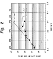
- Fig. 1 shows results of measurement, through an atomic force microscope (AFM), of standard deviation (RMS (Root Mean Square)) in height of periodic undulations appearing on layer surfaces (typically extending in the ⁇ 1-10 ⁇ direction) when a semiconductor light emitting device using II-VI compound semiconductors is fabricated by growing a cladding layer, optical guide layer, active layer, p-type contact layer, and so on, by MBE while changing ratios of molecular beam intensities of group VI elements relative to molecular beam intensities of group II elements (VI/II ratios).
- AFM atomic force microscope
- RMS Root Mean Square
- VI/II ratio (fSe+0.3xfZnS+fO+fTe)/(fZn+fCd+fMg+fHg+fBe +fZnS) where fx is the intensity of the molecular beam intensity of a source material x (supplied amount of x).
- the invention has been made based on the above-mentioned studies.
- a semiconductor light emitting device comprising:
- the active layer may have undulations in a part thereof.
- the standard deviation in height of undulations of the active layer is typically 1 to 3 nm.
- a method for manufacturing a semiconductor light emitting device having:
- the semiconductor light emitting device typically includes a first optical guide layer between the n-type cladding layer and the active layer and a second optical guide layer between the p-type cladding layer and the active layer.
- the first and second optical guide layers are made of a II-VI compound semiconductor containing at least one of group II elements selected from the group consisting of Zn, Cd, Mg, Hg and Be and at least one of group VI elements selected from the group consisting of S, Se, Te and O
- the n-type cladding layer, first optical guide layer, active layer, second optical guide layer and p-type cladding layer are grown by varying, for the respective layers, the ratio of the molecular beam intensity of the group VI element relative to the molecular beam intensity of the group II element.
- the semiconductor light emitting device typically includes a p-type contact layer on the p-type cladding layer.
- the p-type contact layer is made of a II-VI compound semiconductor containing at least one of group II elements selected from the group consisting of Zn, Cd, Mg, Hg and Be and at least one of group VI elements selected from the group consisting of S, Se, Te and O
- the n-type cladding layer, active layer, p-type cladding layer and p-type contact layer are grown by varying, for the respective layer, the ratio of the molecular intensity of the group VI element relative to the molecular intensity of the group II element.
- the active layer in order to ensure that undulations be made at least in the active layer and the p-type contact layer be flat, the active layer, at least, is grown by setting the ratio of the molecular beam intensity of the group VI element relative to the molecular intensity of the group II element to a value not lower than 0.6 and lower than 1.0, and the p-type contact layer is grown by setting the ratio of the molecular beam intensity of the group VI element relative to the molecular intensity of the group II element to a value not lower than 1.0 and not higher than 1.2.
- undulations may be made by growth in the layer immediately under the active layer so that undulations appear in the active layer even when the active layer itself is grown under normal conditions other than those for making undulations.
- the ratio of the molecular intensity of the group VI element relative to the molecular beam intensity of the group II element for growth of the p-type cladding layer is set to a value not less than 0.9
- the ratio of the molecular intensity of the group VI element relative to the molecular beam intensity of the group II element for growth of at least the latter of the first optical guide layer and the second optical guide layer is set to a value not less than 1
- the ratio of the molecular intensity of the group VI element relative to the molecular beam intensity of the group II element for growth of the active layer is set to a value not less than 0.9 and not more than 1.1.
- an optical recording and/or reproducing apparatus using a semiconductor light emitting device in which the semiconductor light emitting device comprises:
- the active layer has undulations, for example, having a height whose standard deviation is 1 to 3 nm, the lifetime of the active layer can be maximized. Additionally, since the p-type contact layer is flat, the lifetime of the p-side electrode in contact with the p-type contact layer is maximized.
- undulations whose standard deviation in height is 1 to 3 nm can be made in the active layer by setting the ratio of the molecular beam intensity of the group VI element relative to the molecular beam intensity of the group II element for growth of the active layer to a value of 0.6 to 1.0, while the p-type contact layer is made flat by setting the ratio of the molecular beam intensity of the group VI element relative to the molecular beam intensity of the group II element for growth of the p-type contact layer on the p-type cladding layer to a value of 1.0 to 1.2.
- Fig. 7 shows a semiconductor laser taken as the first embodiment of the invention.
- the semiconductor laser has an SCH structure.
- n-type GaAs substrate 1 doped with Si, for example, as an n-type impurity and having the (001) face orientation, for example.
- Sequentially grown on the substrate 1 are an n-type ZnSe buffer layer 2, n-type ZnSe buffer layer 3, n-type ZnSSe buffer layer 4, n-type ZnMgSSe cladding layer 5, n-type ZnSSe optical guide layer 6, active layer 7 of a single quantum well (SQW) structure or a multiquantum well (MQW) structure having undoped ZnCdSe layers, for example, as its quantum well layers, p-type ZnSSe optical guide layer 8, p-type ZnMgSSe cladding layer 9, p-type ZnSSe cap layer 10, p-type ZnSe contact layer 11, p-type ZnSe/ZnTe MQW layer 12, and p-type ZnTe contact layer
- the n-type GaAs buffer layer 2 is 0.5 ⁇ m thick, for example, and doped with Si, for example, as an n-type impurity.
- the n-type ZnSe buffer layer 3 is 30 nm thick, for example, and doped with Cl, for example, as an n-type impurity.
- the n-type ZnSSe buffer layer 4 is 50 nm thick, for example, and doped with Cl, for example, as an n-type impurity.
- the n-type ZnMgSSe cladding layer 5 is 0.8 ⁇ m thick, for example, and doped with Cl, for example, as an n-type impurity.
- the n-type ZnSSe optical guide layer 6 is 45 nm thick, for example, and doped with Cl, for example, as an n-type impurity.
- the p-type ZnSSe optical guide layer 8 is 45 nm thick, for example, and doped with N, for example, as a p-type impurity.
- the p-type ZnMgSSe cladding layer 9 is 1 ⁇ m thick, for example, and doped with N, for example, as a p-type impurity.
- the p-type ZnSSe cap layer 10 is 400 nm thick, for example, and doped with N, for example, as a p-type impurity.
- the p-type ZnSe contact layer 11 is 200 nm thick, for example, and doped with N, for example, as a p-type impurity.
- the p-type ZnSe layers and p-type ZnTe layers forming the p-type ZnSe/ZnTe MQW layer 12 are doped with N, for example, as a p-type impurity.
- the p-type ZnTe contact layer 13 is 100 nm thick, for example, and doped with N, for example, as a p-type impurity.
- An upper-lying portion of the p-type ZnSSe cap layer 10, p-type ZnSe contact layer 11, p-type ZnSe/ZnTe MQW layer 12 and p-type ZnTe contact layer 13 have the form of a stripe extending in one direction (for example, ⁇ 1-10 ⁇ direction).
- An insulating layer 14 which may be an Al 2 O 3 layer, is formed on the area of the p-type ZnSSe cap layer 10 excluding the stripe portion, so as to form a current blocking structure.
- the insulating layer 14 may be made of polyimide, for example.
- a p-side electrode 15 of a Pd/Pt/Au structure for example, in ohmic contact with the p-type ZnTe contact layer 13.
- an n-side electrode 16 such as In electrode, is formed in ohmic contact.
- the n-type ZnSe buffer layer 3, n-type ZnSSe buffer layer 4, n-type ZnMgSSe cladding layer 5, n-type ZnSSe optical guide layer 6 and active layer 7 include undulations extending substantially in parallel.
- the standard deviation (RMS) in height of the undulations in these layers is 1 to 3 nm.
- the extending direction of these undulations is ⁇ 1-10 ⁇ , and their wavelength direction is ⁇ 110 ⁇ .
- the n-type GaAs substrate 1 is set on a substrate holder in a highly evacuated vacuum container of a MBE apparatus, not shown, for growth of III-V compound semiconductors.
- the n-type GaAs substrate 1 is heated to a predetermined growth temperature, 560°C, for example, and the n-type GaAs buffer layer 2 is grown on the n-type GaAs substrate 1 by MBE.
- Si molecular beam sources Knudsen cells
- the surface of the n-type GaAs substrate 1 may be cleaned by heating the substrate to a temperature around 580°C, for example, to remove a surface oxide film, or the like, from its surface by thermal etching.
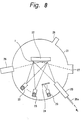
- the n-type GaAs substrate having the n-type GaAs buffer layer 2 thereon is moved from the MBE apparatus for growth of III-V compound semiconductors through a vacuum transport path (not shown) into a MBE apparatus for growth of II-VI compound semiconductors shown in Fig. 8.
- a vacuum transport path not shown
- II-VI compound semiconductors forming the laser structure are grown.
- the surface of the n-type GaAs buffer layer 2 remains clean without being exposed to ambient air while moved to the MBE apparatus.
- a substrate holder 22 is provided in a vacuum container 21 highly evacuated by a super-high evacuator (not shown), and the substrate for growth of layers thereon is put on the substrate holder 22.
- the vacuum container 21 also contains a plurality of molecular beam sources (Knudsen cells) 23 supported in confrontation with the substrate holder 22.
- the molecular beam sources 23 used here are sources of Zn, Se, Mg, ZnS, Cd, Te, ZnCl 2 , and so forth.
- These molecular beam sources 23 are valve cells in which valves can be opened and closed to control intensities of molecular beams generated from the molecular beam sources 23.
- the vacuum container 21 also contains a plasma cell 25 using electron cyclotron resonance (ECR) or radio frequency (RF) oriented toward the substrate holder 22.
- ECR electron cyclotron resonance
- RF radio frequency
- the vacuum container 21 further contains a reflection high energy electron diffraction (RHEED) electron gun 26 and a fluorescent screen 27 so that a RHEED image can be observed.
- RHEED reflection high energy electron diffraction
- Also contained in the vacuum container 21 is a quadrupole mass analyzer 28.
- the n-type GaAs substrate 1 having the n-type GaAs buffer layer 2 grown thereon is set on the substrate holder 22 in the vacuum container 21 of the MBE apparatus shown in Fig. 8. Then, the growth by MBE is started, keeping the n-type GaAs substrate n-type GaAs substrate 1 at a predetermined growth temperature, approximately, 250°C, for example.
- n-type GaAs buffer layer 2 sequentially grown on the n-type GaAs buffer layer 2 are the n-type ZnSe buffer layer 3, n-type ZnSSe buffer layer 4, n-type ZnMgSSe cladding layer 5, n-type ZnSSe optical guide layer 6, active layer 7, p-type ZnSSe optical guide layer 8, p-type ZnMgSSe cladding layer 9, p-type ZnSSe cap layer 10, p-type ZnSe contact layer 11, p-type ZnSe/ZnTe MQW layer 12, and p-type ZnTe contact layer 13.
- the Vi/II ratio of molecular beams used for the growth is set and maintained at a value not less than 0.6 and less than 1.0, namely, 0.8, for example.
- the VI/II ratio of molecular beams used for the growth is set to a value not less than 1.0 and not larger than 1.2, namely, 1.1, for example.
- Control of the VI/II ratio during growth of these II-VI compound semiconductor layers is made by controlling the molecular beam intensities by opening and closing valves of valve cells used as the molecular beam sources 23.
- n-type ZnSSe buffer layer 4 For doping Cl as the n-type impurity of the n-type ZnSe buffer layer 3, n-type ZnSSe buffer layer 4, n-type ZnMgSSe cladding layer 5 and n-type ZnSSe optical guide layer, ZnCl 2 , for example, is used as the dopant.
- N 2 gas introduced through a nitrogen gas inlet tube 25a is changed into plasma in the plasma cell 25 of the MBE apparatus shown in Fig. 8, and the N 2 plasma is irradiated onto the substrate surface.
- a stripe-shaped resist pattern (not shown) is applied onto the p-type ZnTe contact layer 13 by lithography, and the product is etched by wet etching, for example, using the resist pattern as a mask, to the depth reaching a middle portion of the p-type ZnSSe cap layer 10 in its thickness direction.
- the upper-lying portion of the p-type ZnSSe cap layer 10, p-type ZnSe contact lawyer 11, p-type ZnS/ZnTe MQW layer 12 and p-type ZnTe contact layer 13 are patterned into a stripe extending in the ⁇ 110 ⁇ direction.
- the Al 2 O 3 film is formed on the entire surface of the product by vacuum evaporation, or the like. Then, the resist pattern is removed together with the overlying portion of the Al 2 O 3 film (lift off) . As a result, the insulating layer 14 is formed at both sides of the stripe-patterned upper portion of the p-type ZnSSe cap layer 10, p-type ZnSe contact layer 11, p-type ZnSe/ZnTe MQW layer 12 and p-type ZnTe contact layer 13.
- the p-side electrode 15 of a Pd/Pt/Au structure is made by sequentially depositing a Pd film, Pt film and Au film on the entire surface of the stripe-shaped p-type ZnTe contact layer 13 and the insulating layer 14 at opposite sides of the contact layer 14 by vacuum evaporation, for example. If necessary, annealing follows to bring the p-side electrode 15 into ohmic contact with the p-type ZnTe contact layer 13. Formed on the bottom surface of the n-type GaAs substrate 1 is the n-side electrode 16 such as In electrode.
- the n-type GaAs substrate 1 having the laser structure thereon is cloven into bars to expose opposite cavity end surfaces, and, after applying an end coating, if necessary, the bars are cloven into chips.
- the laser chip, thus, obtained, is mounted on a heat sink for packaging. As a result, the intended semiconductor laser is obtained.
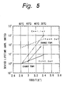
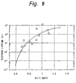
- Fig. 9 shows results of measurement of changes in lifetime of the p-side electrode 15 with the VI/II ratio upon growing layers forming the semiconductor laser by MBE. It is known from Fig. 9 that the lifetime of the p-side electrode 15 is maximized to approximately 1000 hours when the VI/II ratio is around 1.1.
- the lifetime of the active layer 7 is maximized when the VI/II ratio is around 0.8.
- the lifetime of the active layer 7 is maximized.
- the p-type ZnSe contact layer 11 in contact with the p-side electrode 15 p-type ZnSe/ZnTe MQW layer 12 and p-type ZnTe contact layer 13 are made flat, the lifetime of the p-side electrode 15 is maximized. As a result, the lifetime of the semiconductor light emitting device can be elongated remarkably, and its characteristics and reliability can be improved.
- Fig. 10 shows a semiconductor laser taken as the second embodiment of the invention.
- the n-type ZnSe buffer layer 3, n-type ZnSSe buffer layer 4, n-type ZnMgSSe cladding layer 5 and n-type ZnSSe optical guide layer 6 include undulations extending substantially in parallel.
- the standard deviation (RMS) in height of the undulations in these layers is 1 to 3 nm.
- the extending direction of these undulations is ⁇ 1-10 ⁇ , and their wavelength direction is ⁇ 110 ⁇ .
- the semiconductor laser is the same as that of the first embodiment, and explanation thereof is omitted here.
- the n-type GaAs buffer layer 2 is grown on the n-type GaAs substrate 1 in the same manner as the first embodiment.
- n-type ZnSe buffer layer 3 Next grown on the n-type GaAs buffer layer 2 in the MBE apparatus shown in Fig. 8 are, in sequence, the n-type ZnSe buffer layer 3, n-type ZnSSe buffer layer 4, n-type ZnMgSSe cladding layer 5, n-type ZnSSe optical guide layer 6, active layer 7, p-type ZnSSe optical guide layer 8, p-type ZnMgSSe cladding layer 9, p-type ZnSSe cap layer 10, p-type ZnSe contact layer 11, p-type ZnSe/ZnTe MQW layer 12, and p-type ZnTe contact layer 13.
- the VI/II ratio of molecular beams used for the growth is set and maintained at approximately 0.95.
- the VI/II ratio of molecular beams used for the growth is set and maintained at approximately 0.9.
- the VI/II ratio of molecular beams used for the growth is set and maintained at approximately 0.95.
- the VI/II ratio of molecular beams used for the growth is set and maintained at approximately 1.05. This value results in suppressing deterioration of the active layer 7 itself and in improving the device lifetime.
- the VI/II ratio of molecular beams used for the growth is set to approximately 1.1.
- the p-type ZnSSe cap layer 10, p-type ZnSe contact layer 11, p-type ZnSe/ZnTe MQW layer 12, and p-type ZnTe contact layer 13 are made flat.
- the lifetime of the p-side electrode 15 is improved.
- Selection of these VI/II ratios can be attained by opening and closing the valve of the molecular beam source 23 of Se, for example, to adjust the molecular beam intensity of Se.
- the intended semiconductor laser is obtained.
- the lifetime of the semiconductor laser can be elongated remarkably, and its characteristics and reliability can be improved.
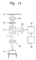
- FIG. 11 shows a construction of the optical disc reproducing apparatus.
- the optical disc reproducing device includes a semiconductor laser 101 as its light emitting device.
- the semiconductor 101 used here is one explained with the first or second embodiment.
- the optical disc reproducing apparatus further includes a known optical system for introducing light from the semiconductor laser 101 to an optical disc D and for reproducing light reflected from the optical disc (signal light), namely, collimator lens 102, beam splitter 103, 1/4 wavelength plate 104, object lens 105, detector lens 106, signal light detecting element 107, and signal light reproducing circuit 108.
- output light L from the semiconductor laser 101 is shaped into parallel beams of light by the choriomata lens 102, passing through the beam splitter 103, adjusted in polarization by the 1/4 wavelength plate 104, and focused onto the optical disc D by the object lens 105.
- this optical disc reproducing apparatus uses the long-lifetime semiconductor laser according to the first or second embodiment as its semiconductor laser, also the optical disc reproducing apparatus can be elongated in lifetime.
- the above explanation has been made as applying the semiconductor laser according to the first or second embodiment to a light emitting device of an optical disc reproducing apparatus, it is applicable to a light emitting device of any other optical apparatus, such as optical disc record/reproducing apparatus, optical transmission apparatus, and so forth, and also to a light emitting device of car-borne device operated in a high temperature condition, video display, or the like.
- the first embodiment has been described as setting and maintaining the VI/II ratio of molecular beams in the range not less than 0.6 and less than 1.0 until completing the growth of the n-type ZnSe buffer layer 3, n-type ZnSSe buffer layer 4, n-type ZnMgSSe cladding layer 5, n-type ZnSSe optical guide layer 6 and active layer 7, and as setting and maintaining the VI/II ratio of molecular beams in the range not lower than 1.0 and lower than 1.2 during the later growth of the p-type ZnSSe optical guide layer 8, p-type ZnMgSSe cladding layer 9, p-type ZnSSe cap layer 10, p-type ZnSe contact layer 11, p-type ZnSe/ZnTe MQW layer 12 and p-type ZnTe contact layer 13.
- VI/II ratio in the range not lower than 0.6 and lower than 1.0 for growth of layers from the n-type ZnSe buffer layer 3 to the lower half of the p-type ZnSSe cap layer 10, and use a VI/II ration in the range not lower than 1.0 and not higher than 1.2 for subsequent growth of the remainder half of the p-type ZnSSe cap layer 10, p-type ZnSe contact layer 11, p-type ZnSe/ZnTe MQW layer 12 and p-type ZnTe contact layer 13.
- the n-type ZnSe buffer layer 3, n-type ZnSSe buffer layer 4 and n-type ZnMgSSe cladding layer 5 alone may be grown under undulation-making conditions, and all the other upper layers may be grown under flat-making conditions.
- the n-type ZnSSe optical guide layer 6 alone may be grown under undulation-making conditions, and all the other layers may be grown under flat-making conditions.
- VI/II ratios may be controlled by using a plurality of molecular beam sources 23 of Se or Zn, for example, to use an appropriate number of these molecular beam sources 23 during growth of respective II-VI compound semiconductor layers.
- first and second embodiments have been described as applying the invention to a semiconductor laser having an SCH structure, the invention is also applicable to a semiconductor laser having a DH structure (Double Heterostructure). Further, although the embodiments have been described as allying the invention to a semiconductor laser, the invention is also applicable to a light emitting diode.
- the semiconductor light emitting device includes undulations at least in its active layer whilst the p-type contact layer is flat, it realizes excellent characteristics, a high reliability and a long lifetime.
- the method for manufacturing a semiconductor light emitting device according to the invention uses appropriate values of the ratio of the group VI element molecular beam intensity relative to the group II element molecular beam intensity, respectively, for growth of the n-type cladding layer, active layer and p-type cladding layer, a semiconductor light emitting device having excellent characteristics, a high reliability and a long lifetime can be obtained.
- the optical recording and/or reproducing apparatus can be elongated in its own lifetime by using a long-lifetime semiconductor light emitting device according to the invention.
Landscapes
- Physics & Mathematics (AREA)
- Optics & Photonics (AREA)
- Engineering & Computer Science (AREA)
- Nanotechnology (AREA)
- Chemical & Material Sciences (AREA)
- Condensed Matter Physics & Semiconductors (AREA)
- General Physics & Mathematics (AREA)
- Electromagnetism (AREA)
- Biophysics (AREA)
- Crystallography & Structural Chemistry (AREA)
- Life Sciences & Earth Sciences (AREA)
- Semiconductor Lasers (AREA)
- Led Devices (AREA)
Applications Claiming Priority (3)
| Application Number | Priority Date | Filing Date | Title |
|---|---|---|---|
| JP33620896 | 1996-11-11 | ||
| JP336208/96 | 1996-11-11 | ||
| JP33620896 | 1996-11-11 |
Publications (2)
| Publication Number | Publication Date |
|---|---|
| EP0841707A2 true EP0841707A2 (fr) | 1998-05-13 |
| EP0841707A3 EP0841707A3 (fr) | 2000-05-03 |
Family
ID=18296758
Family Applications (1)
| Application Number | Title | Priority Date | Filing Date |
|---|---|---|---|
| EP97119653A Withdrawn EP0841707A3 (fr) | 1996-11-11 | 1997-11-10 | Dispositif semi-conducteur émetteur de lumière, méthode de fabrication et appareil d'enregistrement et de lecture optique |
Country Status (3)
| Country | Link |
|---|---|
| US (1) | US5898662A (fr) |
| EP (1) | EP0841707A3 (fr) |
| KR (1) | KR19980042282A (fr) |
Cited By (2)
| Publication number | Priority date | Publication date | Assignee | Title |
|---|---|---|---|---|
| EP0863555A3 (fr) * | 1997-03-07 | 1999-07-07 | Japan Science and Technology Corporation | Elément optique à semi-conducteur et procédé de fabrication |
| DE19964499B4 (de) * | 1998-10-26 | 2011-02-03 | Epistar Corp. | Ohmscher Kontakt zu Halbleitervorrichtungen und ein Verfahren zum Herstellen desselben |
Families Citing this family (3)
| Publication number | Priority date | Publication date | Assignee | Title |
|---|---|---|---|---|
| DE10058444A1 (de) * | 2000-11-24 | 2002-06-06 | Infineon Technologies Ag | Halbleiterlaserelement und Verfahren zur Herstellung eines Halbleiterlaserelements |
| US8298856B2 (en) * | 2008-07-17 | 2012-10-30 | Uriel Solar, Inc. | Polycrystalline CDTE thin film semiconductor photovoltaic cell structures for use in solar electricity generation |
| CA2780175A1 (fr) * | 2009-12-10 | 2011-06-16 | Uriel Solar Inc. | Structures de cellules photovoltaiques a semi-conducteur a couche mince de cdte polycristallin a haut rendement energetique destinees a etre utilisees dans la generation d'electricite solaire |
Family Cites Families (9)
| Publication number | Priority date | Publication date | Assignee | Title |
|---|---|---|---|---|
| JP2625695B2 (ja) * | 1987-01-07 | 1997-07-02 | ソニー株式会社 | ▲iii▼−▲v▼族或は▲ii▼−▲vi▼族化合物半導体のエピタキシヤル成長法 |
| US5150191A (en) * | 1989-11-21 | 1992-09-22 | Kabushiki Kaisha Toshiba | P-type II-VI compound semiconductor doped |
| US5515393A (en) * | 1992-01-29 | 1996-05-07 | Sony Corporation | Semiconductor laser with ZnMgSSe cladding layers |
| JP3116675B2 (ja) * | 1993-07-28 | 2000-12-11 | ソニー株式会社 | 半導体レーザー |
| US5705831A (en) * | 1994-04-07 | 1998-01-06 | Matsushita Electric Industrial Co., Ltd. | Semiconductor light-emitting device and production method thereof, and crystal-growing method suitable for the production method |
| JPH0897519A (ja) * | 1994-07-29 | 1996-04-12 | Sony Corp | 半導体発光装置 |
| JP3233330B2 (ja) * | 1994-08-23 | 2001-11-26 | 松下電器産業株式会社 | 半導体発光素子及びその製造方法 |
| JPH08115877A (ja) * | 1994-10-17 | 1996-05-07 | Sony Corp | 半導体エピタキシャル成長方法 |
| JPH0997803A (ja) * | 1995-09-29 | 1997-04-08 | Sony Corp | カドミウムを含むii−vi族化合物半導体層およびその成長方法 |
-
1997
- 1997-11-10 EP EP97119653A patent/EP0841707A3/fr not_active Withdrawn
- 1997-11-10 US US08/967,095 patent/US5898662A/en not_active Expired - Fee Related
- 1997-11-11 KR KR1019970059240A patent/KR19980042282A/ko not_active Withdrawn
Cited By (3)
| Publication number | Priority date | Publication date | Assignee | Title |
|---|---|---|---|---|
| EP0863555A3 (fr) * | 1997-03-07 | 1999-07-07 | Japan Science and Technology Corporation | Elément optique à semi-conducteur et procédé de fabrication |
| EP1555698A1 (fr) * | 1997-03-07 | 2005-07-20 | Japan Science and Technology Corporation | Elément optique à semi-conducteur et procédé de fabrication |
| DE19964499B4 (de) * | 1998-10-26 | 2011-02-03 | Epistar Corp. | Ohmscher Kontakt zu Halbleitervorrichtungen und ein Verfahren zum Herstellen desselben |
Also Published As
| Publication number | Publication date |
|---|---|
| KR19980042282A (ko) | 1998-08-17 |
| EP0841707A3 (fr) | 2000-05-03 |
| US5898662A (en) | 1999-04-27 |
Similar Documents
| Publication | Publication Date | Title |
|---|---|---|
| US6392979B1 (en) | Optical pickup and optical disk apparatus using the same | |
| US6072817A (en) | Semiconductor laser device and optical disk apparatus using the same | |
| US6891189B2 (en) | Nitride semiconductor laser device and optical pickup apparatus therewith | |
| EP0683924B1 (fr) | Procédé pour fabriquer un contact ohmique à composition proportionnée pour semi-conducteurs II-VI de type p | |
| JP2007324607A (ja) | Ii−vi族化合物半導体レーザダイオード | |
| US5898662A (en) | Semiconductor light emitting device, its manufacturing method and optical recording and/or reproducing apparatus | |
| EP0766297A2 (fr) | Méthode de croissance d'une couche semi-conductrice de composé II-VI contenant du cadmium et méthode de fabrication d'un laser à semi-conducteur | |
| JPH09116234A (ja) | 半導体装置 | |
| EP0867948A2 (fr) | Dispositif semi-conducteur émetteur de lumière, méthode de fabrication et dispositif optique | |
| JPH11150334A (ja) | 半導体発光素子 | |
| JPH10190154A (ja) | 半導体発光素子およびその製造方法ならびに光記録および/または光再生装置 | |
| JPH10303514A (ja) | 半導体発光素子およびその製造方法 | |
| KR100459579B1 (ko) | 베릴륨을함유한ⅱ-ⅵ족청색-녹색레이저다이오드 | |
| JPH09293937A (ja) | 半導体発光素子 | |
| JPH09232688A (ja) | 半導体発光素子 | |
| JPH10326944A (ja) | 半導体装置の製造方法 | |
| JPH09162500A (ja) | 半導体発光素子 | |
| JPH10154850A (ja) | 垂直共振器型半導体発光素子、発光装置、光ディスク装置、記録装置、及びエッチング方法 | |
| JPH07273054A (ja) | Ii−vi族化合物半導体の成長方法 | |
| JPH1083999A (ja) | ヘテロエピタキシャル半導体結晶構造体、その製造方法、その製造装置、半導体発光素子およびこれを用いた光ディスク装置 | |
| JPH10200216A (ja) | 半導体発光素子およびそれを用いた光ディスク装置 | |
| JPH08288311A (ja) | 半導体積層構造およびその製造方法 | |
| JPH11150333A (ja) | 半導体発光素子 | |
| JP2000031592A (ja) | 半導体発光素子 | |
| JPH09246289A (ja) | 半導体装置およびその製造方法 |
Legal Events
| Date | Code | Title | Description |
|---|---|---|---|
| PUAI | Public reference made under article 153(3) epc to a published international application that has entered the european phase |
Free format text: ORIGINAL CODE: 0009012 |
|
| AK | Designated contracting states |
Kind code of ref document: A2 Designated state(s): DE FR GB |
|
| AX | Request for extension of the european patent |
Free format text: AL;LT;LV;MK;RO;SI |
|
| PUAL | Search report despatched |
Free format text: ORIGINAL CODE: 0009013 |
|
| AK | Designated contracting states |
Kind code of ref document: A3 Designated state(s): AT BE CH DE DK ES FI FR GB GR IE IT LI LU MC NL PT SE |
|
| AX | Request for extension of the european patent |
Free format text: AL;LT;LV;MK;RO;SI |
|
| RIC1 | Information provided on ipc code assigned before grant |
Free format text: 7H 01L 33/00 A, 7H 01S 3/19 B, 7H 01L 21/363 B |
|
| 17P | Request for examination filed |
Effective date: 20001006 |
|
| AKX | Designation fees paid |
Free format text: DE FR GB |
|
| STAA | Information on the status of an ep patent application or granted ep patent |
Free format text: STATUS: THE APPLICATION HAS BEEN WITHDRAWN |
|
| 18W | Application withdrawn |
Withdrawal date: 20020429 |