EP0869548A1 - Dispositif semiconducteur soudé sans fil et scellé à la résine - Google Patents
Dispositif semiconducteur soudé sans fil et scellé à la résine Download PDFInfo
- Publication number
- EP0869548A1 EP0869548A1 EP98105868A EP98105868A EP0869548A1 EP 0869548 A1 EP0869548 A1 EP 0869548A1 EP 98105868 A EP98105868 A EP 98105868A EP 98105868 A EP98105868 A EP 98105868A EP 0869548 A1 EP0869548 A1 EP 0869548A1
- Authority
- EP
- European Patent Office
- Prior art keywords
- gold
- aluminum
- semiconductor device
- electrically conductive
- conductive bump
- Prior art date
- Legal status (The legal status is an assumption and is not a legal conclusion. Google has not performed a legal analysis and makes no representation as to the accuracy of the status listed.)
- Withdrawn
Links
Images




Classifications
-
- H—ELECTRICITY
- H10—SEMICONDUCTOR DEVICES; ELECTRIC SOLID-STATE DEVICES NOT OTHERWISE PROVIDED FOR
- H10W—GENERIC PACKAGES, INTERCONNECTIONS, CONNECTORS OR OTHER CONSTRUCTIONAL DETAILS OF DEVICES COVERED BY CLASS H10
- H10W72/00—Interconnections or connectors in packages
- H10W72/20—Bump connectors, e.g. solder bumps or copper pillars; Dummy bumps; Thermal bumps
-
- H—ELECTRICITY
- H10—SEMICONDUCTOR DEVICES; ELECTRIC SOLID-STATE DEVICES NOT OTHERWISE PROVIDED FOR
- H10W—GENERIC PACKAGES, INTERCONNECTIONS, CONNECTORS OR OTHER CONSTRUCTIONAL DETAILS OF DEVICES COVERED BY CLASS H10
- H10W72/00—Interconnections or connectors in packages
- H10W72/20—Bump connectors, e.g. solder bumps or copper pillars; Dummy bumps; Thermal bumps
- H10W72/251—Materials
- H10W72/252—Materials comprising solid metals or solid metalloids, e.g. PbSn, Ag or Cu
-
- H—ELECTRICITY
- H10—SEMICONDUCTOR DEVICES; ELECTRIC SOLID-STATE DEVICES NOT OTHERWISE PROVIDED FOR
- H10W—GENERIC PACKAGES, INTERCONNECTIONS, CONNECTORS OR OTHER CONSTRUCTIONAL DETAILS OF DEVICES COVERED BY CLASS H10
- H10W74/00—Encapsulations, e.g. protective coatings
- H10W74/01—Manufacture or treatment
- H10W74/012—Manufacture or treatment of encapsulations on active surfaces of flip-chip devices, e.g. forming underfills
-
- H—ELECTRICITY
- H10—SEMICONDUCTOR DEVICES; ELECTRIC SOLID-STATE DEVICES NOT OTHERWISE PROVIDED FOR
- H10W—GENERIC PACKAGES, INTERCONNECTIONS, CONNECTORS OR OTHER CONSTRUCTIONAL DETAILS OF DEVICES COVERED BY CLASS H10
- H10W74/00—Encapsulations, e.g. protective coatings
- H10W74/01—Manufacture or treatment
- H10W74/016—Manufacture or treatment using moulds
-
- H—ELECTRICITY
- H10—SEMICONDUCTOR DEVICES; ELECTRIC SOLID-STATE DEVICES NOT OTHERWISE PROVIDED FOR
- H10W—GENERIC PACKAGES, INTERCONNECTIONS, CONNECTORS OR OTHER CONSTRUCTIONAL DETAILS OF DEVICES COVERED BY CLASS H10
- H10W74/00—Encapsulations, e.g. protective coatings
- H10W74/10—Encapsulations, e.g. protective coatings characterised by their shape or disposition
- H10W74/15—Encapsulations, e.g. protective coatings characterised by their shape or disposition on active surfaces of flip-chip devices, e.g. underfills
-
- H—ELECTRICITY
- H10—SEMICONDUCTOR DEVICES; ELECTRIC SOLID-STATE DEVICES NOT OTHERWISE PROVIDED FOR
- H10W—GENERIC PACKAGES, INTERCONNECTIONS, CONNECTORS OR OTHER CONSTRUCTIONAL DETAILS OF DEVICES COVERED BY CLASS H10
- H10W72/00—Interconnections or connectors in packages
- H10W72/071—Connecting or disconnecting
- H10W72/072—Connecting or disconnecting of bump connectors
- H10W72/07251—Connecting or disconnecting of bump connectors characterised by changes in properties of the bump connectors during connecting
-
- H—ELECTRICITY
- H10—SEMICONDUCTOR DEVICES; ELECTRIC SOLID-STATE DEVICES NOT OTHERWISE PROVIDED FOR
- H10W—GENERIC PACKAGES, INTERCONNECTIONS, CONNECTORS OR OTHER CONSTRUCTIONAL DETAILS OF DEVICES COVERED BY CLASS H10
- H10W72/00—Interconnections or connectors in packages
- H10W72/20—Bump connectors, e.g. solder bumps or copper pillars; Dummy bumps; Thermal bumps
- H10W72/251—Materials
-
- H—ELECTRICITY
- H10—SEMICONDUCTOR DEVICES; ELECTRIC SOLID-STATE DEVICES NOT OTHERWISE PROVIDED FOR
- H10W—GENERIC PACKAGES, INTERCONNECTIONS, CONNECTORS OR OTHER CONSTRUCTIONAL DETAILS OF DEVICES COVERED BY CLASS H10
- H10W72/00—Interconnections or connectors in packages
- H10W72/50—Bond wires
- H10W72/551—Materials of bond wires
- H10W72/552—Materials of bond wires comprising metals or metalloids, e.g. silver
- H10W72/5522—Materials of bond wires comprising metals or metalloids, e.g. silver comprising gold [Au]
-
- H—ELECTRICITY
- H10—SEMICONDUCTOR DEVICES; ELECTRIC SOLID-STATE DEVICES NOT OTHERWISE PROVIDED FOR
- H10W—GENERIC PACKAGES, INTERCONNECTIONS, CONNECTORS OR OTHER CONSTRUCTIONAL DETAILS OF DEVICES COVERED BY CLASS H10
- H10W72/00—Interconnections or connectors in packages
- H10W72/50—Bond wires
- H10W72/551—Materials of bond wires
- H10W72/552—Materials of bond wires comprising metals or metalloids, e.g. silver
- H10W72/5524—Materials of bond wires comprising metals or metalloids, e.g. silver comprising aluminium [Al]
-
- H—ELECTRICITY
- H10—SEMICONDUCTOR DEVICES; ELECTRIC SOLID-STATE DEVICES NOT OTHERWISE PROVIDED FOR
- H10W—GENERIC PACKAGES, INTERCONNECTIONS, CONNECTORS OR OTHER CONSTRUCTIONAL DETAILS OF DEVICES COVERED BY CLASS H10
- H10W72/00—Interconnections or connectors in packages
- H10W72/851—Dispositions of multiple connectors or interconnections
- H10W72/853—On the same surface
- H10W72/856—Bump connectors and die-attach connectors
-
- H—ELECTRICITY
- H10—SEMICONDUCTOR DEVICES; ELECTRIC SOLID-STATE DEVICES NOT OTHERWISE PROVIDED FOR
- H10W—GENERIC PACKAGES, INTERCONNECTIONS, CONNECTORS OR OTHER CONSTRUCTIONAL DETAILS OF DEVICES COVERED BY CLASS H10
- H10W72/00—Interconnections or connectors in packages
- H10W72/90—Bond pads, in general
- H10W72/951—Materials of bond pads
- H10W72/952—Materials of bond pads comprising metals or metalloids, e.g. PbSn, Ag or Cu
Definitions
- the semiconductor chip is first mounted on the mounting substrate for electrical connection through conductive lines to the lead frames.
- the resin sealed packaging method for the resin sealing of the semiconductor chip and parts of the lead frame and conducive lines can be used widely as being suitable for mass production.
- FIG. 1 is a fragmentary cross sectional elevation view illustrative of a conventional resin sealed wireless semiconductor device.
- a semiconductor chip 1 has a bottom surface on which aluminum electrode pads 52 are formed.
- Conductive bumps 55 are bonded with the aluminum electrode pads 52 so that the conductive bumps 55 are bonded in face down with a substrate 3 by use of an alloy solder 4 for subsequent resin sealing thereof.
- Gold bumps are usually used as conductive bumps 55 to be connected to the aluminum pads 52 on the semiconductor chip 1.
- Gold has a large spreading property. This means that the gold bump is unlikely to be disconnected even a stress is applied when the resin is filled.
- Gold is also most inactive and highly resistive to corrosion due to impurity and moisture in the resin. Gold is further resistive to oxidation in atmosphere.
- the above wireless semiconductor device has the following disadvantage in formation of an alloy layer between the aluminum electrode pads of the semiconductor device and the gold bumps for electrical connection to the aluminum pads due to an internally generated heat or a high temperature atmosphere.
- This alloy layer weakens the bonding strength in a short time. Further, when the high temperature test is carried out for a long time, Kirkendall voids as crack are formed in the aluminum electrode. As a result, the resin sealed semiconductor device has a disadvantage in remarkable deterioration of connection.
- the semiconductor device In the field for dealing with a large amount of informations in a short time such as multi-media, the semiconductor device is required to be improved in high density integration and high sped performance, for which reason a heat generation from a chip is larger than the traditional ones.
- a junction temperature is not higher than 100°C.
- the traditional semiconductor chips are required to be operable at a temperature of not higher than 125°C even in special field.
- a sealing package such as ceramic package is used for a large scale integrated circuit which has a large power consumption in specific field.
- a heat sink is necessary in those case of the large power consumption to prevent an excess rising of a junction temperature of the semiconductor chip.
- the ceramic packaged semiconductor device is somewhat expensive because the fabrication processes are complicated. It is difficult to replace the ceramic package semiconductor device with the resin sealed semiconductor device in view of the mass productivity and the cost performance. If the heat sink is provided in the resin sealed semiconductor device to prevent an excess junction temperature increase, then the fabrication processes are complicated whereby such the semiconductor device is inferiors in the mass productivity and the cost performance.
- the resin sealed semiconductor device has a heat resistively to a high junction temperature of over 125°C for allowing the mass production of a high speed and high density integrated large scale integrated circuit which generate a large heat and is used in the multi-media.
- the semiconductor device is required to have a heat resistivity to the 150°C junction temperature, then the bonding strength between the gold bumps and aluminum pads is deteriorated. If the junction temperature is maintained over 150°C for a long time, then an alloy layer is grown at the bonding between the aluminum electrode pads and the gold bumps. Such the alloy layer deteriorates the bonding strength between the aluminum electrode pad and the gold wire whereby the gold bump might be removed from the aluminum pads.
- the probability of removal of the gold bump from the aluminum electrode pad depends upon a glass transition temperature of the sealing resin. If the glass transition temperature of the used resin is not higher than 150°C, the provability of the gold bump from the aluminum electrode pad is high. If, however, the glass transition temperature of the used resin is about 200°C, then the provability of the gold bump from the aluminum electrode pad is low.
- the resin having a high glass transition temperature has a low Young's module and is hard but poor flexibility, for which reason such the resin is unsuitable for packaging the semiconductor chip on the substrate. If the resin absorbs a moisture and heated for soldering process, then the moisture in the resin is rapidly vaporized whereby the crack is likely to be generated in the resin.
- the device In practical use, enabling the device to be operable at a junction temperature of not less than 125°C, it is required to carry out an acceleration life-time test as the reliability test at a high temperature of 125°C, particularly in the range of 175-200°C. For efficient and reliable acceleration life-time text, it preferable to carry out the life-time text at a higher temperature by 50 °C than the practically required junction temperature.
- Japanese laid-open patent publication No. 2-91944 it is disclosed to use a gold bump containing Pd at 0.5-15% for facilitation of process of the gold bump. It is also disclosed to use the gold bump containing at 0.0001-0.2 % by weight at least one of La, Ce and Cs.
- noble metal bumps such as gold bump for connection with the aluminum interconnection pattern on the insulation substrate for bonding the semiconductor device to the insulation substrate, whereby an inter-metallic compound of Au 4 Al is formed between the gold bump and the aluminum interconnection.
- FIG. 1 is a fragmentary cross sectional elevation view illustrative of a conventional resin sealed wireless semiconductor device.
- FIG. 2 is a fragmentary cross sectional elevation view illustrative of a wireless semiconductor device.
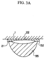
- FIGS. 3A and 3B are fragmentary cross sectional elevation views illustrative of a mechanism of removal of the conductive bump from the aluminum-containing electrode pad.
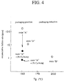
- FIG. 4 is a diagram illustrative of an accumulative failure rate over glass transition temperature Tg.
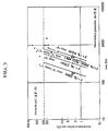
- FIG. 5 is a diagram illustrative of variations of accumulative failure rates over time under a high temperature condition, wherein Al/Si pads are used.
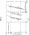
- FIG. 6 is a diagram illustrative of variations of accumulative failure rates over time under a high temperature condition, wherein Al/Si/Cu pads are used.
- a bonding structure of a semiconductor chip to a substrate comprises both a bonding portion including at least an aluminum-containing electrode formed on the semiconductor chip and a gold-containing electrically conductive bump on the aluminum-containing electrode, wherein the bonding portion further includes Pd and Cu.
- the bonding portion may include an alloy layer disposed between the aluminum-containing electrode pad and the gold-containing electrically conductive bump.
- At least any one of the aluminum-containing electrode pad and the gold-containing electrically conductive bump may include Pd.
- Pd may be included at least any one of surface and inner regions of the one of the aluminum-containing electrode pad and the gold-containing electrically conductive bump.
- a semiconductor device which comprises a semiconductor chip, a bonding portion including an aluminum-containing electrode formed on the semiconductor chip and a gold-containing electrically conductive bump on the aluminum-containing electrode, wherein the bonding portion further includes Pd and Cu.
- At least any one of the aluminum-containing electrode pad and the gold-containing electrically conductive bump may include Pd.
- Pd may be included at least any one of surface and inner regions of the one of the aluminum-containing electrode pad and the gold-containing electrically conductive bump.
- a method of forming a bonding structure of a semiconductor chip to a substrate comprises both a bonding portion including at least an aluminum-containing electrode formed on the semiconductor chip and a gold-containing electrically conductive bump on the aluminum-containing electrode, wherein the bonding portion further includes Pd and Cu.
- the bonding portion may include an alloy layer disposed between the aluminum-containing electrode pad and the gold-containing electrically conductive bump.
- At least any one of the aluminum-containing electrode pad and the gold-containing electrically conductive bump may include Pd.
- the aluminum-containing electrode comprises Cu at 0.1-1% and aluminum at substantially the remaining percentage
- the gold-containing electrically conductive bump comprises Pd at 0.5-5% and gold at substantially the remaining percentage and further preferable that the bonding portion has an alloy layer.
- a resin sealed semiconductor device wherein the above semiconductor device is sealed with a sealing resin.
- a resin sealed hybrid semiconductor device wherein a plurality of the above semiconductor devices are sealed with a sealing resin.
- a method of forming a resin sealed semiconductor device which includes a process of sealing the semiconductor device with a sealing resin.
- a glass transition temperature of the sealing resin is controlled to prevent fracture of the resin and deterioration of moisture property du to thermal variation in packaging process.
- FIG. 2 is a fragmentary cross sectional elevation view illustrative of a wireless semiconductor device.
- a semiconductor chip 1 has a bottom surface on which electrode pads of a conductive material including aluminum are formed.
- An insulation substrate 3 has a top surface on which a conductive pattern is formed.
- Conductive bumps 5 are provided for bonding the electrode pads 2 to the substrate. The conductive bumps 5 are fixed on the substrate 3 by a solder 4.
- An insulative resin 6 is filled into a space between the semiconductor chip 1 and the substrate 3.
- the electrode pads 2 may be made of a conductive material such as a pure aluminum, a silicon-doped aluminum, a silicon and copper-doped aluminum, and a copper doped aluminum.
- the conductive bump 5 may be made of a pure gold for a high density semiconductor chip. Notwithstanding, a gold-copper alloy bump and a 1% Pd-containing gold bump are available. Th gold bump 5 is bonded to the aluminum-containing electrode pad 2 and also bonded to the substrate 3.
- the substrate 3 may comprise a printed board, or may have lead frames for electrical contacts.
- the semiconductor chip 1 and the conductive bump 5 are sealed with a molten resin. Alternatively, a solder may be re flowed to seal the semiconductor device onto the insulative substrate 3 or the printed board.
- such the wireless semiconductor device has a resistivity to the solder reflow and is superior in connection reliability between the conductive bump 5 and the aluminum-containing electrode pad 2 at high temperature.
- the improvements of the resin and the gold bump are required for high connection reliability. It is required to standardize the connection reliability between the conductive pad 5 and the aluminum-containing electrode pad 2 in operation of the resin sealed semiconductor device at high temperature.
- a junction temperature Tj between the conductive pad 5 and the aluminum-containing electrode pad 2 is available.
- the junction temperature Tj Ta + Rth ⁇ P0.
- the heat resistivity of the entire of the package is set at about 20°C/W under an atmospheric temperature of 100°C and a power P0 of 1W. It is also confirmed that the connection reliability of the junction portion of the wireless semiconductor device in operation is presumable and can be ensured for a long time, if the connection reliability is ensured at the above junction temperature for over 1000 hours.
- the resin of a higher glass transition temperature than the conventional ones is used and a selected composition of the gold bump is used for obtaining the junction temperature in the range of 125-150°C.
- An amount of silica included in the sealing resin for sealing the semiconductor chip 1 is so set that the glass transition temperature Tg of the sealing resin is in the range of 140-160°C.
- the resin having a glass transition temperature lower than 140°C has a quality for over 1000 hours at the junction temperature of 120 °C. If the glass transition temperature is beyond 160°C, a crack is generated.
- the resin 6 having a glass transition temperature in the range of 140-160°C, it is required to consider a relationship to a stress applied to the conductive bump 5 when sealed with the resin.
- the pure gold bump free of any impurity allows a generation of Kirkendall voids as crack which increases a probability of malfunction when a high temperature storage test is carried out at 150°C. In this case, it is possible to keep the quality of the semiconductor device for 1000 hours.
- the composition of the conductive bump 5 in relation to the above resin 6 it can be confirmed that if gold containing copper or palladium at 1% by weight is used as a bump, the life-time of over 1000 hours at 150°C is ensured a probability of malfunction of the device is remarkable reduced.
- the life-time of the bonding structure of the gold bump and the Al/Si/Cu electrode pad is longer by 2 times than the life-time of the bonding structure of the gold bump and the Al/Si electrode pad.
- the life-time of the bonding structure of the Au/Cu bump and the Al/Si electrode pad is longer by 2.2 times than the life-time of the bonding structure of the gold bump and the Al/Si electrode pad.
- the life-time of the bonding structure of the 1%Pd containing Au bump and the Al/Si/Cu electrode pad is longer by 25.7 times than the life-time of the bonding structure of the gold bump and the Al/Si electrode pad.
- the life-time of the bonding structure of the 1%Pd containing Au bump and the Al/Si/Cu electrode pad is longer by 10.3 times than the life-time of the bonding structure of the gold bump and the Al electrode pad.
- the 1%Pd containing Au bump allows formation of the alloy layer 23 without, however, formation of any Kirkendall void. No Kirkendall void is no cause to remove the bump from the electrode pad, for which reason the 1%Pd containing Au bump allows the bonding structure to have a long life-time.
- FIG. 4 is a diagram illustrative of an accumulative failure rate over glass transition temperature Tg. If the copper free gold bump is sealed with a resin "A" having a glass transition temperature of 150°C, then the accumulative failure rate is 100 ppm. If, however, 1% by weight copper containing gold bump is sealed with this resin "A”, then the accumulative failure rate is less than 10 ppm. If a resin "B" having a glass transition temperature of 200°C is used, the accumulative failure rate is reduced whilst the packageabilty is deteriorated.
- A” Tg 149°C Au/Pd Al/Si/Cu 14200 59800 0.80
- Sample C Resin Bump Pad 150°C 250°C activation energy 10ppm life-time (Hr) "C” Au
- the life-time is extended by 12 times. If the Al-containing electrode pad is replaced by the Al-Si-Cu electrode pad, then the life-time is extended by 2 times.
- FIG. 5 is a diagram illustrative of variations of accumulative failure rates over time under a high temperature condition, wherein Al/Si pads are used.
- FIG. 6 is a diagram illustrative of variations of accumulative failure rates over time under a high temperature condition, wherein Al/Si/Cu pads are used.
- FIG. 7 is a diagram illustrative of variations of accumulative failure rates over time under a high temperature condition, wherein Al/Si/Cu pads are used.
- the life-time is extended by 12 times. If the Au bump is replaced by the Au/Cu bump, then the life-time is extended by 2 times. If the Al/Si electrode pads are replaced by the Al/Si/Cu electrode pads, then the life-time is extended by 2 times.
Landscapes
- Wire Bonding (AREA)
- Structures Or Materials For Encapsulating Or Coating Semiconductor Devices Or Solid State Devices (AREA)
Applications Claiming Priority (2)
| Application Number | Priority Date | Filing Date | Title |
|---|---|---|---|
| JP79720/97 | 1997-03-31 | ||
| JP9079720A JP2962351B2 (ja) | 1997-03-31 | 1997-03-31 | 半導体チップへの接合構造及びそれを用いた半導体装置 |
Publications (1)
| Publication Number | Publication Date |
|---|---|
| EP0869548A1 true EP0869548A1 (fr) | 1998-10-07 |
Family
ID=13698046
Family Applications (1)
| Application Number | Title | Priority Date | Filing Date |
|---|---|---|---|
| EP98105868A Withdrawn EP0869548A1 (fr) | 1997-03-31 | 1998-03-31 | Dispositif semiconducteur soudé sans fil et scellé à la résine |
Country Status (4)
| Country | Link |
|---|---|
| EP (1) | EP0869548A1 (fr) |
| JP (1) | JP2962351B2 (fr) |
| KR (1) | KR19980080940A (fr) |
| CN (1) | CN1198012A (fr) |
Cited By (1)
| Publication number | Priority date | Publication date | Assignee | Title |
|---|---|---|---|---|
| US7193328B2 (en) | 2001-07-05 | 2007-03-20 | Sharp Kabushiki Kaisha | Semiconductor device |
Families Citing this family (4)
| Publication number | Priority date | Publication date | Assignee | Title |
|---|---|---|---|---|
| US7331502B2 (en) * | 2001-03-19 | 2008-02-19 | Sumitomo Bakelite Company, Ltd. | Method of manufacturing electronic part and electronic part obtained by the method |
| TW585015B (en) * | 2001-06-28 | 2004-04-21 | Sanyo Electric Co | Hybrid integrated circuit device and method for manufacturing same |
| US7271497B2 (en) * | 2003-03-10 | 2007-09-18 | Fairchild Semiconductor Corporation | Dual metal stud bumping for flip chip applications |
| JP4305430B2 (ja) * | 2005-08-24 | 2009-07-29 | ソニー株式会社 | 部品実装方法および部品実装体 |
Citations (8)
| Publication number | Priority date | Publication date | Assignee | Title |
|---|---|---|---|---|
| JPS63252445A (ja) * | 1987-04-08 | 1988-10-19 | Fuji Electric Co Ltd | 半導体装置の製造方法 |
| JPS63289947A (ja) * | 1987-05-22 | 1988-11-28 | Toshiba Corp | はんだバンプ付き基板及びその製造方法 |
| JPS63299239A (ja) * | 1987-05-29 | 1988-12-06 | Toshiba Corp | フィルムキャリア型半導体装置及びその製造方法 |
| JPS6415956A (en) * | 1987-07-10 | 1989-01-19 | Nec Corp | Method for forming bump |
| EP0313082A2 (fr) * | 1987-10-21 | 1989-04-26 | Kabushiki Kaisha Toshiba | Dispositif semi-conducteur comprenant une électrode à protubérance et procédé pour sa fabrication |
| JPH02296336A (ja) * | 1989-05-10 | 1990-12-06 | Seiko Epson Corp | 半導体回路バンプの製造方法 |
| DE4442960C1 (de) * | 1994-12-02 | 1995-12-21 | Fraunhofer Ges Forschung | Lothöcker für die Flip-Chip-Montage und Verfahren zu dessen Herstellung |
| EP0704895A2 (fr) * | 1994-09-30 | 1996-04-03 | Nec Corporation | Procédé de fabrication d'un dispositif semi-conducteur et d'un substrat semi-conducteur |
-
1997
- 1997-03-31 JP JP9079720A patent/JP2962351B2/ja not_active Expired - Lifetime
-
1998
- 1998-03-31 KR KR1019980011245A patent/KR19980080940A/ko not_active Ceased
- 1998-03-31 CN CN98100997A patent/CN1198012A/zh active Pending
- 1998-03-31 EP EP98105868A patent/EP0869548A1/fr not_active Withdrawn
Patent Citations (8)
| Publication number | Priority date | Publication date | Assignee | Title |
|---|---|---|---|---|
| JPS63252445A (ja) * | 1987-04-08 | 1988-10-19 | Fuji Electric Co Ltd | 半導体装置の製造方法 |
| JPS63289947A (ja) * | 1987-05-22 | 1988-11-28 | Toshiba Corp | はんだバンプ付き基板及びその製造方法 |
| JPS63299239A (ja) * | 1987-05-29 | 1988-12-06 | Toshiba Corp | フィルムキャリア型半導体装置及びその製造方法 |
| JPS6415956A (en) * | 1987-07-10 | 1989-01-19 | Nec Corp | Method for forming bump |
| EP0313082A2 (fr) * | 1987-10-21 | 1989-04-26 | Kabushiki Kaisha Toshiba | Dispositif semi-conducteur comprenant une électrode à protubérance et procédé pour sa fabrication |
| JPH02296336A (ja) * | 1989-05-10 | 1990-12-06 | Seiko Epson Corp | 半導体回路バンプの製造方法 |
| EP0704895A2 (fr) * | 1994-09-30 | 1996-04-03 | Nec Corporation | Procédé de fabrication d'un dispositif semi-conducteur et d'un substrat semi-conducteur |
| DE4442960C1 (de) * | 1994-12-02 | 1995-12-21 | Fraunhofer Ges Forschung | Lothöcker für die Flip-Chip-Montage und Verfahren zu dessen Herstellung |
Non-Patent Citations (6)
| Title |
|---|
| JING E ET AL: "RELIABILITY INVESTIGATIONS OF DIFFERENT BUMPING PROCESSES FOR FLIP CHIP AND TAB APPLICATIONS", NINETEENTH IEEE/CPMT INTERNATIONAL ELECTRONICS MANUFACTURING TECHNOLOGY SYMPOSIUM, AUSTIN, OCT. 14 - 16, 1996, no. SYMP. 19, 14 October 1996 (1996-10-14), INSTITUTE OF ELECTRICAL AND ELECTRONICS ENGINEERS, pages 274 - 281, XP000704344 * |
| PATENT ABSTRACTS OF JAPAN vol. 013, no. 068 (E - 716) 16 February 1989 (1989-02-16) * |
| PATENT ABSTRACTS OF JAPAN vol. 013, no. 121 (E - 732) 24 March 1989 (1989-03-24) * |
| PATENT ABSTRACTS OF JAPAN vol. 013, no. 132 (E - 736) 31 March 1989 (1989-03-31) * |
| PATENT ABSTRACTS OF JAPAN vol. 013, no. 195 (E - 754) 10 May 1989 (1989-05-10) * |
| PATENT ABSTRACTS OF JAPAN vol. 015, no. 078 (E - 1037) 22 February 1991 (1991-02-22) * |
Cited By (1)
| Publication number | Priority date | Publication date | Assignee | Title |
|---|---|---|---|---|
| US7193328B2 (en) | 2001-07-05 | 2007-03-20 | Sharp Kabushiki Kaisha | Semiconductor device |
Also Published As
| Publication number | Publication date |
|---|---|
| JPH10275810A (ja) | 1998-10-13 |
| KR19980080940A (ko) | 1998-11-25 |
| JP2962351B2 (ja) | 1999-10-12 |
| CN1198012A (zh) | 1998-11-04 |
Similar Documents
| Publication | Publication Date | Title |
|---|---|---|
| EP0847828B1 (fr) | Matériau pour soudure tendre et composant électronique utilisant ledit matériau | |
| US9196562B2 (en) | Semiconductor arrangement, semiconductor module, and method for connecting a semiconductor chip to a ceramic substrate | |
| JP3757881B2 (ja) | はんだ | |
| JP3558063B2 (ja) | はんだ | |
| KR100719905B1 (ko) | Sn-Bi계 솔더 합금 및 이를 이용한 반도체 소자 | |
| US6444562B1 (en) | Nickel alloy films for reduced intermetallic formation in solder | |
| JP2007152385A (ja) | 高温半田及び高温半田ペースト材、及びそれを用いたパワー半導体装置 | |
| US6727587B2 (en) | Connection device and method for producing the same | |
| US8084861B2 (en) | Connection structure semiconductor chip and electronic component including the connection structure and methods for producing the connection structure | |
| US8399996B2 (en) | Chip carrier | |
| JP3527356B2 (ja) | 半導体装置 | |
| US20050032348A1 (en) | Method of wafer bumping for enabling a stitch wire bond in the absence of discrete bump formation | |
| JP2005259915A (ja) | 半導体装置およびその製造方法 | |
| KR100333573B1 (ko) | 전극용금속합금을구비한반도체장치 | |
| JP2962351B2 (ja) | 半導体チップへの接合構造及びそれを用いた半導体装置 | |
| EP0100817A2 (fr) | Boîtier à scellement hermétique pour un élément électrique et procédé de fabrication | |
| JPH10303235A (ja) | 半導体素子ボンディング用金合金線 | |
| US20250210574A1 (en) | Semiconductor device, power device, and power module | |
| JPS5961054A (ja) | 半導体装置 | |
| JPS6351649A (ja) | 半導体装置 | |
| JPS6129139A (ja) | 半導体装置 | |
| JPH02174253A (ja) | 金属部にレニウム層を有する電子部品パッケージ | |
| JP2000124390A (ja) | Icパッケージ | |
| JPS6175548A (ja) | 半導体装置 | |
| JPH09503888A (ja) | 縁部接続可能な金属パッケージ |
Legal Events
| Date | Code | Title | Description |
|---|---|---|---|
| PUAI | Public reference made under article 153(3) epc to a published international application that has entered the european phase |
Free format text: ORIGINAL CODE: 0009012 |
|
| AK | Designated contracting states |
Kind code of ref document: A1 Designated state(s): DE FR GB |
|
| 17P | Request for examination filed |
Effective date: 19980819 |
|
| AKX | Designation fees paid |
Free format text: DE FR GB |
|
| STAA | Information on the status of an ep patent application or granted ep patent |
Free format text: STATUS: THE APPLICATION HAS BEEN WITHDRAWN |
|
| 18W | Application withdrawn |
Withdrawal date: 20010619 |