EP0872886A2 - Plastikverkapselte Halbleitervorrichtung und Herstellungsmethode - Google Patents
Plastikverkapselte Halbleitervorrichtung und Herstellungsmethode Download PDFInfo
- Publication number
- EP0872886A2 EP0872886A2 EP98107028A EP98107028A EP0872886A2 EP 0872886 A2 EP0872886 A2 EP 0872886A2 EP 98107028 A EP98107028 A EP 98107028A EP 98107028 A EP98107028 A EP 98107028A EP 0872886 A2 EP0872886 A2 EP 0872886A2
- Authority
- EP
- European Patent Office
- Prior art keywords
- island
- package
- chip
- plastic
- semiconductor device
- Prior art date
- Legal status (The legal status is an assumption and is not a legal conclusion. Google has not performed a legal analysis and makes no representation as to the accuracy of the status listed.)
- Withdrawn
Links
Images








Classifications
-
- H—ELECTRICITY
- H10—SEMICONDUCTOR DEVICES; ELECTRIC SOLID-STATE DEVICES NOT OTHERWISE PROVIDED FOR
- H10W—GENERIC PACKAGES, INTERCONNECTIONS, CONNECTORS OR OTHER CONSTRUCTIONAL DETAILS OF DEVICES COVERED BY CLASS H10
- H10W74/00—Encapsulations, e.g. protective coatings
- H10W74/10—Encapsulations, e.g. protective coatings characterised by their shape or disposition
- H10W74/111—Encapsulations, e.g. protective coatings characterised by their shape or disposition the semiconductor body being completely enclosed
-
- H—ELECTRICITY
- H10—SEMICONDUCTOR DEVICES; ELECTRIC SOLID-STATE DEVICES NOT OTHERWISE PROVIDED FOR
- H10W—GENERIC PACKAGES, INTERCONNECTIONS, CONNECTORS OR OTHER CONSTRUCTIONAL DETAILS OF DEVICES COVERED BY CLASS H10
- H10W70/00—Package substrates; Interposers; Redistribution layers [RDL]
- H10W70/40—Leadframes
- H10W70/461—Leadframes specially adapted for cooling
-
- H—ELECTRICITY
- H10—SEMICONDUCTOR DEVICES; ELECTRIC SOLID-STATE DEVICES NOT OTHERWISE PROVIDED FOR
- H10W—GENERIC PACKAGES, INTERCONNECTIONS, CONNECTORS OR OTHER CONSTRUCTIONAL DETAILS OF DEVICES COVERED BY CLASS H10
- H10W72/00—Interconnections or connectors in packages
- H10W72/01—Manufacture or treatment
- H10W72/0198—Manufacture or treatment batch processes
-
- H—ELECTRICITY
- H10—SEMICONDUCTOR DEVICES; ELECTRIC SOLID-STATE DEVICES NOT OTHERWISE PROVIDED FOR
- H10W—GENERIC PACKAGES, INTERCONNECTIONS, CONNECTORS OR OTHER CONSTRUCTIONAL DETAILS OF DEVICES COVERED BY CLASS H10
- H10W74/00—Encapsulations, e.g. protective coatings
- H10W74/01—Manufacture or treatment
- H10W74/016—Manufacture or treatment using moulds
-
- H—ELECTRICITY
- H10—SEMICONDUCTOR DEVICES; ELECTRIC SOLID-STATE DEVICES NOT OTHERWISE PROVIDED FOR
- H10W—GENERIC PACKAGES, INTERCONNECTIONS, CONNECTORS OR OTHER CONSTRUCTIONAL DETAILS OF DEVICES COVERED BY CLASS H10
- H10W72/00—Interconnections or connectors in packages
- H10W72/50—Bond wires
- H10W72/541—Dispositions of bond wires
- H10W72/5449—Dispositions of bond wires not being orthogonal to a side surface of the chip, e.g. fan-out arrangements
-
- H—ELECTRICITY
- H10—SEMICONDUCTOR DEVICES; ELECTRIC SOLID-STATE DEVICES NOT OTHERWISE PROVIDED FOR
- H10W—GENERIC PACKAGES, INTERCONNECTIONS, CONNECTORS OR OTHER CONSTRUCTIONAL DETAILS OF DEVICES COVERED BY CLASS H10
- H10W72/00—Interconnections or connectors in packages
- H10W72/90—Bond pads, in general
- H10W72/931—Shapes of bond pads
- H10W72/932—Plan-view shape, i.e. in top view
-
- H—ELECTRICITY
- H10—SEMICONDUCTOR DEVICES; ELECTRIC SOLID-STATE DEVICES NOT OTHERWISE PROVIDED FOR
- H10W—GENERIC PACKAGES, INTERCONNECTIONS, CONNECTORS OR OTHER CONSTRUCTIONAL DETAILS OF DEVICES COVERED BY CLASS H10
- H10W74/00—Encapsulations, e.g. protective coatings
-
- H—ELECTRICITY
- H10—SEMICONDUCTOR DEVICES; ELECTRIC SOLID-STATE DEVICES NOT OTHERWISE PROVIDED FOR
- H10W—GENERIC PACKAGES, INTERCONNECTIONS, CONNECTORS OR OTHER CONSTRUCTIONAL DETAILS OF DEVICES COVERED BY CLASS H10
- H10W74/00—Encapsulations, e.g. protective coatings
- H10W74/10—Encapsulations, e.g. protective coatings characterised by their shape or disposition
-
- H—ELECTRICITY
- H10—SEMICONDUCTOR DEVICES; ELECTRIC SOLID-STATE DEVICES NOT OTHERWISE PROVIDED FOR
- H10W—GENERIC PACKAGES, INTERCONNECTIONS, CONNECTORS OR OTHER CONSTRUCTIONAL DETAILS OF DEVICES COVERED BY CLASS H10
- H10W90/00—Package configurations
- H10W90/701—Package configurations characterised by the relative positions of pads or connectors relative to package parts
- H10W90/751—Package configurations characterised by the relative positions of pads or connectors relative to package parts of bond wires
- H10W90/756—Package configurations characterised by the relative positions of pads or connectors relative to package parts of bond wires between a chip and a stacked lead frame, conducting package substrate or heat sink
Definitions
- the present invention relates to a semiconductor device and more particularly, to a plastic-encapsulated semiconductor device having a good heat dissipation performance and a good moisture resistance, and a fabrication method thereof.
- plastic-encapsulated semiconductor devices have been used in various electronic equipment.
- an Integrated circuit (IC) or Large-Scale Integrated circuit (LSI) chip or pellet is encapsulated in a plastic package and electrically-conductive leads or terminals are protruded from the package. These leads are electrically connected to boding pads of the IC chips within the package. If the semiconductor device is mounted on a circuit board and the leads or terminals are electrically connected to wiring lines of the circuit board, various input signals may be applied to the IC chip or pellet and various output signals may be derived therefrom.
- IC Integrated circuit
- LSI Large-Scale Integrated circuit
- the semiconductor devices of this sort have been practically used in various application fields. With the semiconductor devices designed for outputting the electric wave in portable or pocket telephones, electric power consumption generates a lot of heat on operation and therefore, the heat thus generated needs to be efficiently dissipated or radiated.
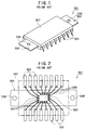
- Figs. 1 and 2 show a conventional plastic-encapsulated semiconductor device 501 capable of efficient heat dissipation. This device is disclosed in the Japanese Non-Examined Patent Publication No. 61-144834 published in 1986.
- this plastic-encapsulated semiconductor device 501 is equipped with an approximately square IC chip or pellet 503 having bonding pads 502 on its top face.
- the chip 503 is mounted on an island 504.
- the island 504 is formed by a rectangular metallic plate and the chip 503 is fixed onto the center of an upper side of the island 504.
- Leads or terminals 505 are arranged at regular intervals on the long sides of the island 504.
- the leads 505 are electrically connected to the corresponding bonding pads 502 of the chip 503 through bonding wires 506.
- the IC chip or pellet 503, the island 504, the leads 505, and the bonding wires 506 are encapsulated or molded in a rectangular parallelepiped-shaped plastic package 507 while the outer parts of the leads 505 and the short-side ends of the island 504 are protruded from the package 507.
- the protruding outer parts of the leads 505 are located at the long sides of the package 507.
- the protruding ends of the island 504 have penetrating circular holes 508.
- the conventional semiconductor device shown in Figs. 1 and 2 is mounted, for example, on an upper side of a wiring board (not shown) with the use of screws inserted into the penetrating holes 508 of the island 504.
- the leads or terminals 505 are electrically connected to wiring lines formed on the upper side of the wiring board.
- Various electric signals are transferred between the chip 503 and the wiring lines through the terminals 505.
- the heat generated in the chip 503 is dissipated at the protruding ends of the island 504 from the package 507.
- the heat generated in the IC chip 503 is dissipated through the island 504.
- the protruding parts of the island 4 from the package 507 are apart from the bottom of the package 507. Therefore, conventionally, to improve the heat dissipation performance or capability, a proper thermally-conductive spacer is sandwiched between the protruding ends of the island 504 and the circuit board, or a proper heat-releasing plate is fixed onto the top of the package 507.
- the conventional semiconductor device 501 has no satisfactory heat-dissipation performance.
- the semiconductor devices of this sort designed for the portable telephones have been required to be mounted on a wiring board as flat as possible in view of downsizing, the conventional semiconductor device 501 is not as flat as required.
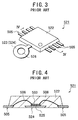
- Figs. 3 and 4 show another conventional plastic-encapsulated semiconductor device 521, which solves the above-described problems in the conventional plastic-encapsulated semiconductor device 501.
- This device is disclosed in the Japanese Non-Examined Patent Publication No, 2-63142 published in 1990.
- this plastic-encapsulated semiconductor device 521 is equipped with a heat-releasing plate 523 with a circular-ringed shape.
- the heat-releasing plate 523 is protruded from one side of a plastic package 522 from which the leads or terminals 505 are not protruded.
- the heat-releasing plate 523 is formed to be incorporated with an island 524.
- the heat-releasing plate 523 is located on a same plane as a middle part 525 of the island 524 on which the IC chip 503 is mounted. As clearly shown in Fig. 4, the middle part 525 of the island 524 is exposed from the bottom face of the package 522. The inner parts of the leads or terminals 505, which are arranged at each side of the island 524, are also exposed from the bottom face of the package 522.
- the conventional semiconductor device 521 is able to be mounted as flat as required for the portable telephones.
- the heat-releasing plate 523 has a circular penetrating hole 526.
- the conventional semiconductor device 521 is mounted on a wiring board (not shown) with the use of a screw inserted into the hole 526.
- the leads 505 can be directly fixed onto the wiring lines of a wiring board by solder joints.
- the semiconductor device 521 is mounted on a wiring board by fixing the heat-releasing plate 523 protruding from the package 522 onto the wiring board with the use of a screw and fixing the island 524 onto a grounding wiring line of the wiring board.
- the middle part 525 of the island 524 is located on an electrically conductive pattern of the wiring board, the middle part 525 can be connected to the pattern by an adhesive with a good thermal conductivity.
- the heat generated in the IC chip 503 is efficiently transmitted to the pattern of the wiring board through the heat-releasing plate 523 and the middle part 525 of the island 524.
- the heat-generating chip 503 is efficiently cooled.
- the conventional semiconductor device 521 shown in Figs. 3 and 4 has the following problems.
- the thermally-conductive adhesive tends to flow toward the leads or terminals 525 before curing and therefore, contact or connection failure of the terminals 525 will occur.
- the terminals 525 may be connected to the wiring lines of the wiring board by solder joints in a soldering process of the terminals 525, instead of the thermally conductive adhesive. In this case, however, a solder is difficult to flow into the narrow gap between the bottom face of the package 522 and the upper surface of the wiring board. Thus, even if the middle part 525 of the island 524 is exposed from the package 522, heat dissipation through the middle part 525 of the island 524 is not practically expected.
- the exposure of the middle part 525 of the island 524 increases the possibility that the moisture contained in the atmosphere reaches the IC chip 503 through the exposed middle part 525.
- the moisture will facilitate (a) disconnection or release of the bonding wires 506, (b) electrical short-circuit between the terminals or leads 505 due to the migration phenomenon, and (c) time-dependent degradation of the chip 503, thereby decreasing the lifetime of the semiconductor device 521.
- the high-frequency electric signals are transferred through a part of the leads or terminals 505.
- interference tends to occur between the leads 505 for the high-frequency electric signals and the remaining leads 505 adjoining thereto.
- grounded terminals or leads are additionally provided at each side of the leads 505 for the high-frequency electric signals.
- an object of the present invention is to provide a plastic-encapsulated semiconductor device capable of efficient heat dissipation without upsizing while preventing the moisture from reaching an IC chip and a fabrication method of the device.
- Another object of the present invention is to provide a semiconductor device that prevents electric isolation between leads or terminals from degrading due to high-frequency electric signals and a fabrication method of the device.
- a plastic-encapsulated semiconductor device which is comprised of an electrically-conductive island having a chip-mounting area, an IC chip fixed on the chip-mounting area of the island, leads electrically connected to bonding pads of the chip through bonding wires, a plastic package for encapsulating the island, the chip, the bonding wires, and inner parts of the leads.
- the package has an approximately flat bottom face.
- Outer parts of the leads are protruded from the package and are located in approximately a same plane as the bottom face of the package.
- the island has an exposition part exposed from the package at a location excluding the chip-mounting area.
- a lower face of the exposition part of the island is located in approximately a same plane as the bottom face of the package.
- the chip and the chip-mounting area of the island are entirely buried in the package.
- a part of the island excluding the chip-mounting area is bent toward the bottom face of the package to be exposed therefrom.
- the island has the exposition part which is exposed from the plastic package, and the lower face of the exposition part is located in approximately a same plane as the bottom face of the package. Therefore, if the semiconductor device is mounted on a substrate such as a wiring board so that the exposition part of the island is connected to an electrically-conductive pattern of the substrate by a thermally-conductive joint such as a solder joint, the heat generated in the IC chip on operation is efficiently dissipated through the electrically-conductive pattern of the substrate.
- the IC chip mounted on the chip-mounting area of the island is entirely buried in the package. Therefore, the moisture contained in the atmosphere is difficult to reach the chip.
- an additional lead is provided for grounding.
- the additional lead is incorporated with the island.
- the additional lead is arranged to be adjacent to a corresponding one of the leads designed for a high-frequency electric signal, there is an additional advantage that electric isolation between the additional lead and the corresponding one of the leads designed for the high-frequency electric signal is prevented from degrading.
- an upper face of the exposition part of the island is exposed from the package.
- the package has a depression formed to expose an upper face of the exposition part of the island from the package.
- the lower face of the exposition part of the island is wider than an upper face of the exposition part of the island.
- the exposition part of the island is protruded from the package.
- a fabrication method of the plastic-encapsulated semiconductor device according to the first aspect is provided, which is comprised of the following steps (a) to (h).
- the leadframe prepared in the step (a) has the set of the island and the lead fingers mechanically connected to the body of the leadframe.
- the exposition area is positioned at the location excluding the chip-mounting area.
- the plastic package is formed by molding the molten encapsulation material into the cavity of the molding die and curing the encapsulation material through the steps (e), (f), and (g).
- the cavity is formed so that the island, the chip, the bonding wires, and the inner parts of the lead fingers are buried in the package while the outer parts of the lead fingers are protruded from the package. Also, The cavity is formed in the following way.
- the package has an approximately flat bottom face and the outer parts of the lead finger are located in approximately a same plane as the bottom face of the package.
- the exposition part of the island is exposed from the package at a location excluding the chip-mounting area.
- a lower face of the exposition part of the island is located in approximately a same plane as the bottom face of the package.
- the plastic-encapsulated semiconductor device according to the first aspect of the present invention is fabricated without adding special processes.
- the cavity of the molding die has a space allowing the exposition part of the island to be exposed from the package.
- the leadframe is prepared in the step (a) in such a way that the exposition part of the island and the inner parts of the lead fingers are depressed or protruded with respect to the outer parts of the lead fingers.
- chip-mounting area of the island and the inner parts of the lead fingers are located in a same plane without any dedicated process for bending the chip-mounting area of the island and/or the inner parts of the lead fingers.
- the leadframe is formed so that the island includes an additional lead for grounding in the step (a).
- the additional lead is incorporated with the island.
- the cavity of the molding die has a space allowing the supplied and cured encapsulating material to form a burr with a predesigned thickness.
- Fig. 1 is a perspective view of a conventional plastic-encapsulated semiconductor device.
- Fig. 2 is a plan view of the conventional plastic-encapsulated semiconductor device shown in Fig. 1, which shows the inner configuration.
- Fig. 3 is a perspective view of another conventional plastic-encapsulated semiconductor device.
- Fig. 4 is a cross-sectional view of the conventional plastic-encapsulated semiconductor device shown in Fig. 3, which is along the line IV-IV.
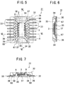
- Fig. 5 is a plan view of a plastic-encapsulated semiconductor device according to a first embodiment of the present invention, which shows the inner configuration.
- Fig. 6 is a cross-sectional view of the plastic-encapsulated semiconductor device according to the first embodiment, which is along the line VI-VI in Fig. 5.
- Fig. 7 is a cross-sectional view of the plastic-encapsulated semiconductor device according to the first embodiment, which is along the line VII-VII in Fig. 5.
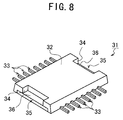
- Fig. 8 is a perspective view of the plastic-encapsulated semiconductor device according to the first embodiment shown in Fig. 5, which shows the appearance.
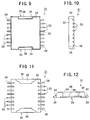
- Fig. 9 is a plan view of the plastic-encapsulated semiconductor device according to the first embodiment shown in Fig. 5.
- Fig. 10 is a side view of the plastic-encapsulated semiconductor device according to the first embodiment shown in Fig. 5.
- Fig. 11 is a bottom view of the plastic-encapsulated semiconductor device according to the first embodiment shown in Fig. 5.
- Fig. 12 is a front view of the plastic-encapsulated semiconductor device according to the first embodiment shown in Fig. 5.
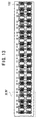
- Fig. 13 is a partial plan view of a leadframe used for fabricating the plastic-encapsulated semiconductor device according to the first embodiment shown in Fig. 5.
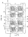
- Fig. 14 is an enlarged, partial plan view of the leadframe used for fabricating the plastic-encapsulated semiconductor device according to the first embodiment shown in Fig. 5, which shows the location XIV in Fig. 13.
- Fig. 15 is a partial cross-sectional view of coupled pressing dies along the line XV-XV in Fig. 14, in which the leadframe is sandwiched by the coupled pressing dies.
- Fig. 16 is a partial cross-sectional view of the coupled pressing dies along the line XVI-XVI in Fig. 14, in which the leadframe is sandwiched by the coupled pressing dies.
- Fig. 17 is a partial plan view of the leadframe used for fabricating the plastic-encapsulated semiconductor device according to the first embodiment shown in Fig. 5, in which an IC chip is mounted on the island of the leadframe.
- Fig. 18 is a cross-sectional view along the line XVIII-XVIII in Fig. 17.
- Fig. 19 is a partial plan view of the leadframe used for fabricating the plastic-encapsulated semiconductor device according to the first embodiment shown in Fig. 5, in which the leadframe is sandwiched between the coupled molding dies.
- Fig. 20 is a cross-sectional view along the line XX-XX in Fig. 19.
- Fig. 21 is a cross-sectional view along the line XXI-XXI in Fig. 19.
- Fig. 22 is a partial plan view showing the state where the plastic package of the semiconductor device according to the first embodiment shown in Fig. 5 is molded.
- Fig. 23 is a partial side view showing the state where the plastic package of the semiconductor device according to the first embodiment shown in Fig. 5 is molded.
- Fig. 24 is a partial bottom view showing the state where the plastic package of the semiconductor device according to the first embodiment shown in Fig. 5 is molded.
- Fig. 25 is a partial plan view showing the state where the encapsulating material left in the injection gates of the molding dies is removed in fabrication of the semiconductor device according to the first embodiment shown in Fig. 5.
- Fig. 26 is a partial side view showing the state where the encapsulating material left in the injection gates of the molding dies is removed in fabrication of the semiconductor device according to the first embodiment shown in Fig. 5.
- Fig. 27 is a partial plan view showing the state where the tie bars of the leadframe are cut away in fabrication of the semiconductor device according to the first embodiment shown in Fig. 5.
- Fig. 28 is a partial side view showing the state where the tie bars of the leadframe are cut away in fabrication of the semiconductor device according to the first embodiment shown in Fig. 5.
- Fig. 29 is a partial plan view showing the state where solder layers are formed on the outer parts of the leads and the exposition areas of the island of the leadframe in fabrication of the semiconductor device according to the first embodiment shown in Fig. 5.
- Fig. 30 is a partial plan view showing the state where solder layers are formed on the outer parts of the leads and the exposition areas of the island of the leadframe in fabrication of the semiconductor device according to the first embodiment shown in Fig. 5.
- Fig. 31 is a partial plan view showing the state where the island supports of the leadframe are cut away in fabrication of the semiconductor device according to the first embodiment shown in Fig. 5.
- Fig. 32 is a partial side view showing the state where the island supports of the leadframe are cut away in fabrication of the semiconductor device according to the first embodiment shown in Fig. 5.
- Fig. 33 is a plan view of a plastic-encapsulated semiconductor device according to a second embodiment of the present invention, which shows the inner configuration.
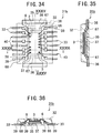
- Fig. 34 is a plan view of a plastic-encapsulated semiconductor device according to a third embodiment of the present invention having grounding leads or terminals, which shows the inner configuration.
- Fig. 35 is a cross-sectional view of the plastic-encapsulated semiconductor device according to the third embodiment, which is along the line XXXV-XXXV in Fig. 34.
- Fig. 36 is a cross-sectional view of the plastic-encapsulated semiconductor device according to the third embodiment, which is along the line XXXVI-XXXVI in Fig. 34.
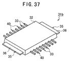
- Fig. 37 is a perspective view of the plastic-encapsulated semiconductor device according to the third embodiment shown in Fig. 34, which shows the appearance.
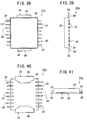
- Fig. 38 is a plan view of the plastic-encapsulated semiconductor device according to the third embodiment shown in Fig. 34.
- Fig. 39 is a side view of the plastic-encapsulated semiconductor device according to the third embodiment shown in Fig. 34.
- Fig. 40 is a bottom view of the plastic-encapsulated semiconductor device according to the third embodiment shown in Fig. 34.
- Fig. 41 is a front view of the plastic-encapsulated semiconductor device according to the third embodiment shown in Fig. 34.
- Fig. 42 is a plan view of a plastic-encapsulated semiconductor device according to a fourth embodiment of the present invention having grounding lead or terminals, which shows the inner configuration.
- Fig. 43 is a cross-sectional view of the plastic-encapsulated semiconductor device according to the fourth embodiment, which is along the line XXXXIII-XXXXIII in Fig. 42.
- Fig. 44 is a cross-sectional view of the plastic-encapsulated semiconductor device according to the fourth embodiment, which is along the line XXXXVI-XXXXVI in Fig. 42.
- Fig. 45 is a perspective view of the plastic-encapsulated semiconductor device according to the fourth embodiment shown in Fig. 42, which shows the appearance.
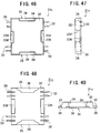
- Fig. 46 is a plan view of the plastic-encapsulated semiconductor device according to the fourth embodiment shown in Fig. 42.
- Fig. 47 is a side view of the plastic-encapsulated semiconductor device according to the fourth embodiment shown in Fig. 42.
- Fig. 48 is a bottom view of the plastic-encapsulated semiconductor device according to the fourth embodiment shown in Fig. 42.
- Fig. 49 is a front view of the plastic-encapsulated semiconductor device according to the fourth embodiment shown in Fig. 42.
- Fig. 50 is a plan view of a plastic-encapsulated semiconductor device according to a fifth embodiment of the present invention having grounding lead or terminals, which shows the inner configuration.
- Fig. 51 is a cross-sectional view of the plastic-encapsulated semiconductor device according to the fifth embodiment, which is along the line XXXXXI-XXXXI in Fig. 50.
- Fig. 52 is a cross-sectional view of the plastic-encapsulated semiconductor device according to the fifth embodiment, which is along the line XXXXXI-XXXXI in Fig. 50.
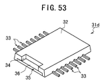
- Fig. 53 is a perspective view of the plastic-encapsulated semiconductor device according to the fifth embodiment shown in Fig. 50, which shows the appearance.
- Fig. 54 is a plan view of the plastic-encapsulated semiconductor device according to the fifth embodiment shown in Fig. 50.
- Fig. 55 is a side view of the plastic-encapsulated semiconductor device according to the fifth embodiment shown in Fig. 50.
- Fig. 56 is a bottom view of the plastic-encapsulated semiconductor device according to the fifth embodiment shown in Fig. 50.
- Fig. 57 is a front view of the plastic-encapsulated semiconductor device according to the fifth embodiment shown in Fig. 50.
- Fig. 58 is a plan view of a plastic-encapsulated semiconductor device according to a sixth embodiment of the present invention having grounding lead or terminals, which shows the inner configuration.
- Fig. 59 is a cross-sectional view of the plastic-encapsulated semiconductor device according to the sixth embodiment, which is along the line XXXXXI-XXXXXI in Fig. 58.
- Fig. 60 is a cross-sectional view of the plastic-encapsulated semiconductor device according to the sixth embodiment, which is along the line XXXXXII-XXXXXII in Fig. 58.
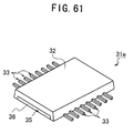
- Fig. 61 is a perspective view of the plastic-encapsulated semiconductor device according to the sixth embodiment shown in Fig. 58, which shows the appearance.
- Fig. 62 is a plan view of the plastic-encapsulated semiconductor device according to the sixth embodiment shown in Fig. 58.
- Fig. 63 is a side view of the plastic-encapsulated semiconductor device according to the sixth embodiment shown in Fig. 58.
- Fig. 64 is a bottom view of the plastic-encapsulated semiconductor device according to the sixth embodiment shown in Fig. 58.
- Fig. 65 is a front view of the plastic-encapsulated semiconductor device according to the sixth embodiment shown in Fig. 58.
- Figs. 5 to 12 show a plastic-encapsulated semiconductor device 31 according to a first embodiment.
- the plastic-encapsulated semiconductor device 31 As shown in Figs. 5 to 12, the plastic-encapsulated semiconductor device 31 according to the first embodiment is equipped with an approximately rectangular island 35, a rectangular parallelepiped-shaped IC chip 3, leads 33 arranged in parallel, and an approximately rectangular parallelepiped-shaped plastic package 32.
- the island 35 is formed by an electrically-conductive sheet metal.
- the island 35 is comprised of a rectangular chip-mounting part 37 located at its center, two end parts 36 located at its opposite ends, and two connection parts 67 located between the chip-mounting part 37 and the two end parts 36.
- the end parts 36 are wider than the chip-mounting part 37.
- connection parts 67 are oblique to the chip-mounting part 37 and the end parts 36 while the chip-mounting part 37 is parallel to the end parts 36.
- the chip-mounting part 37 is bent with respect to the connection parts 67
- the end parts 36 are bent with respect to the connection parts 67. Therefore, it may be said that the island 35 has an arch-shaped longitudinal cross section.
- the IC chip 3 is fixed onto the chip-mounting part 37 of the island 35.
- Bonding pads 2 are regularly arranged on the top face or the chip 3.
- the bonding pads 2 are electrically connected to the inner ends of the corresponding leads 33 through bonding wires 6.
- the leads 33 are arranged at regular intervals on the long sides of the elongated island 35 and the plastic package 32.
- Each of the leads 33 is comprised of a bonding part 38 located at its inner end, a terminal part 39 located at its outer end, and a connection part 68 located between the bonding part 38 and the terminal part 39.
- connection parts 68 of the leads are oblique to the bonding parts 38 and the terminal parts 39 thereof while the bonding parts 38 are parallel to the terminal parts 39.
- the bonding parts 38 are bent with respect to the connection parts 68
- the terminal parts 39 are bent with respect to the connection parts 68. Therefore, it may be said that each of the leads 33 has a crank-shaped longitudinal cross section.
- the bonding parts 38 of the leads 33 are located in the same plane as the chip-mounting part 37 of the island 35.
- the terminal parts 39 of the leads 33 are located in the same plane as the end parts 36 of the island 35.
- the plastic package 32 has two depressions 34 at its opposite ends, which allow the upper faces of the end parts 36 of the island 35 to be partially exposed.
- Each of the depressions 34 is shaped to an approximately rectangular parallelepiped.
- the chip-mounting part 37 of the island 35, the IC chip 3, and the bonding wires 6 are entirely encapsulated or buried in the plastic package 32.
- the end parts 36 of the island 35 are not protruded from the package 32, and are partially exposed from the package 32 through the depressions 34.
- the bonding parts 38 and the connection parts 68 of the leads 33 are entirely buried in the package 32.
- the terminal parts 39 of the leads 33, which are partially buried in the package 32, are laterally protruded from the package 32 through the two opposite long sides of the package 32.
- the lower faces of the end parts 36 of the island 35 are located in the same plane as the bottom face of the package 32, and are exposed from the package 32.
- the terminal parts 39 of the leads 33 are located in the same plane as the bottom face of the package 32, and are exposed from the package 32.
- the exposed area of the lower faces of the end parts 36 of the island 35 is wider than the upper faces of the end parts 36.
- the plastic-encapsulated semiconductor device 31 according to the first embodiment has the following advantages.
- the semiconductor device 31 according to the first embodiment is typically mounted on a printed wiring board (not shown).
- the terminal parts 39 of the leads 33 protruding from the plastic package 32 are electrically connected to corresponding wiring lines of the wiring board by solder joints.
- the two end parts 36 of the island 35 partially exposed from the package 32 are electrically connected to a grounding line or lines or an electrically-conductive pattern of the wiring board by solder joints.
- the chip 3 On operation where various electric signals are transmitted between the IC chip 3 of the semiconductor device 31 and the wiring board, the chip 3 generates heat.
- the heat is efficiently dissipated, because the exposed end parts 36 of the island 35 are directly connected to the electrically-conductive pattern of the wiring board. In other words, the island 35 has a better heat-dissipation capability.
- the middle part 525 of the island 524, on which the IC chip 503 is mounted is exposed from the bottom face of the plastic package 522.
- the island 524 is unable to be connected to the electrically-conductive pattern of the wiring board by a solder joint. Accordingly, the middle part 525 is apart from the electrically-conductive pattern and as a result, the heat-dissipation capability is difficult to be improved.
- the moisture contained in the atmosphere is extremely difficult reach the chip 3 through the gap between the island 35 and the package 32. This is because the chip-mounting part 37 of the island 35 is not exposed from the package 32.
- the semiconductor device 31 according to the first embodiment has a good heat-dissipation capability equivalent to the conventional semiconductor device 521 while preventing the moisture in the atmosphere from reaching the IC chip 3.
- the end parts 36 of the island 35 which are located at the opposite ends along the longitudinal axis of the rectangular parallelpiped-shaped package 32, are exposed from the package 32. Also, the island 35 are bent like a crank at the connection parts 67 in the package 32. Therefore, the moisture in the atmosphere is more difficult to reach the IC chip 3.
- the island 35 may be electrically connected to the electrically-conductive pattern of the wiring board at the depressions 34 of the package 32 by solder joints. In this case, the heat-dissipation capability is further increased.
- the upper faces of the end parts 36 of the island 35 which are not covered with the wiring board, are narrower than the lower faces thereof. This enhances the protection effect against the moisture entering while keeping the heat-dissipation capability unchanged.
- a leadframe 102 including a lot of sets 101 of the island 35 and the leads 33 is prepared by etching a thin metal sheet.
- the island 35 is mechanically connected to a body 105 of the leadframe 102 by island supports 104, and the leads 33 are mechanically connected to the body 105 by tie bars or dam bars 103.
- the leads 33 are mechanically connected to one another by the tie bars 103.
- the reference numeral 128 denotes pilot holes of the leadframe 102 used for transferring the leadframe 102.
- the set 101 of the island 35 and the leads 33 is subjected to a pressure forming process using upper and lower pressing dies 107 and 108 of a down set 106, thereby bending the island 35 and the leads 33 at the connection parts 67 and 68.
- the leadframe 102 is held at the body 105 by the pressing dies 107 and 108.
- the two end parts 36 of the island 35 are bent upward with respect to the chip-mounting part 37 and at the same time, the bonding parts 38 of the leads 33 are bent upward with respect to the terminal parts 39. Due to the bending, the end parts 36 of the island 35 are located in the same plane as the bonding parts 38 of the leads 33, and the chip-mounting part 37 of the island 35 are located in the same plane as the terminal parts 39 of the leads 33.
- the IC chip 3 is fixed onto the chip-mounting part 37 of the island 35 by a solder joint 109. Then, the bonding pads 2 of the chip 3 are electrically connected to the bonding parts 38 of the leads 33 by the bonding wires 6.
- the set 101 of the leadframe 102 is subjected to a molding process. Specifically, the island 35, the chip 3, the bonding wires 2, and the leads 33 are sandwiched between upper and lower molding dies 111 and 112. The island 35, the chip 3, and the bonding wires 2 are entirely located in a cavity 113 of the molding dies 111 and 112. The inner parts of the leads 33 are located in the cavity 113 while the remaining parts of the leads 33 and the tie bars 103 are held by the molding dies 111 and 112 and located outside the cavity 113.
- the part of the cavity 113 corresponding to the two depressions 34 of the package 32 are filled with the molding dies 111 and 112, allowing the depressions 34 to be formed in the following molding process.
- the reference numeral 114 denotes gates of the molding dies 111 and 112 through which a molten molding or encapsulating material is injected into the cavity 113.
- the reference numeral 129 denotes holding or contacting areas of the molding dies 111 and 112 at which the leadframe 102 is fixed by the molding dies 111 and 112. The holding or contacting areas 129 are located in the peripheral area surrounding the cavity 113.
- a molten molding or encapsulating material such as an epoxy resin is injected into the cavity 113 of the molding dies 107 and 108 through the gates 114 until the cavity 113 is filled with the material.
- the injected molding material is then cured, resulting in the plastic package 32 including the island 35, the IC chip 3, the bonding wires 6, and the inner parts of the leads 33.
- the end parts 36 of the island 35 and the terminal parts 39 of the leads 33 which have been held by the molding dies 111 and 112, are exposed from the package 32.
- the bottom face of the package 32 is flat and at the same time, the end parts 36 of the island 35 and the terminal parts 39 of the leads 33 are located in the same flat plane as the bottom face of the package 32. Therefore, the inner surface of the lower molding die 112 may be simply flat. Also, the inner surface of the upper molding die 111 may be simply shaped to form the depressions 34 of the package 32. As a result, there is an additional advantage that the molding dies 111 and 112 are readily fabricated and that high accuracy is not needed in the coupling process of the dies 111 and 112.
- This molding process produces plate-shaped burrs 115 at the position corresponding to the interface of the coupled molding dies 111 and 112 and thin burrs 116 at the position corresponding to the interface of the end parts 36 of the island 35 and the lower molding die 112.
- the thin burrs 116 may be removed by known processes such as water honing and dry blasting processes.
- the plate-shaped burrs 115 may be removed in the step of removing the molding material or resin 117 left in the gates 114 and the island supports 104.
- the molding dies 111 and 112 are so designed that the plate-shaped burrs 115 have a larger thickness than intervening parts between the package 32 and the burrs 115, the burrs 115 may be removed more readily and surely by cutting the thinner intervening parts.
- the plastic package 32 is placed on a table 121 of a punching machine 122. Then, the molding material 117 left in the gates 114 is cut away by using a cutter 122 of the punching machine 122.
- the tie bars 103 are successively cut away by using a cutter 123 and a cutting table 124.
- tie bars 103 are successively cut away by using the single cutter 123 here, they may be cut away simultaneously by using a plurality of cutters 123.
- solder films 125 are formed on the exposed terminal parts 39 of the leads 33 and the exposed end parts 36 of the island 35, the terminal parts 39 and the end parts 36 are subjected to a plating process of solder.
- the plated solder films 125 have a function of preventing the terminal parts 39 of the leads 33 and the end parts 36 of the island 35 from being oxidized and a function of improving the affinity of the leads 33 and the island 35 to solder.
- plastic-encapsulated semiconductor device 31 according to the first embodiment shown in Figs. 5 to 12 is fabricated.
- the configuration where the lower faces of the end parts 36 of the island 35 are exposed from the bottom face of the package 32 and the upper faces thereof are exposed from the two depressions 34 of the package 32 is readily achieved.
- the above configuration is readily achieved without adding any special or dedicated process. Also, the amount of the plate-shaped burrs 115 becomes low and the burrs 115 ace readily removed.
- the leads 33 and the island 35 are bent in the pressing formation process of the leadframe 102, no dedicated tools are necessary for bending the leads 33 and the island 35.
- the leads 33 are bent prior to the separation process from the body 105 of the leadframe 102 and therefore, good shape uniformity of the terminal parts 39 of the leads 33 is ensured. Because the terminal parts 39 of the leads 33 are not bent after the molding process, there is no danger that the package 32 is damaged due to useless stresses.
- the terminal parts 39 of the leads 33 can be located in the same plane as the bottom face of the package 32 and at the same time, the bonding parts 38 of the leads 33 can be located in the same plane as the chip-mounting part 37 of the island 35.
- Fig. 33 shows a plastic-encapsulated semiconductor device 31a according to a second embodiment.
- the device 31a according to the second embodiment has a same configuration as the device 31 according to the first embodiment, except that grounding leads 40 are provided instead of the corresponding leads 33. Therefore, the explanation relating to the same configuration is omitted here by adding the same reference numerals to the same or corresponding elements in Fig. 33.
- the device 31a has the same advantages as those in the first embodiment.
- Each of the grounding leads 40 is formed by a bonding part 38a, a terminal part 39a, and a connection part 68a between the parts 38a and 39a.
- the grounding leads 40 which are incorporated with the island 35, are bent at the connection parts 68a in the same way as the leads 33.
- grounding leads 40 with the island 35 enables a simple configuration and ensures the grounding connection.
- grounding leads 40 and the end parts 37 of the island 35 are electrically connected to ground lines or an electrically-conductive pattern of a wiring board. It is preferred that the grounding leads 40 are located to be adjacent to the leads 33 designed for high-frequency electric signals, because there is an additional advantage that electric isolation between the leads 33 and 40 is improved.
- the grounding leads 40 are formed in advance to be incorporated with the leadframe 102 together with the leads 33. In this case, the productivity is increased because a wire bonding process for the grounding leads 40 are not needed.
- Figs. 34 to 41 show a plastic-encapsulated semiconductor device 31b according to a third embodiment.
- the device 31b according to the third embodiment has a same configuration as the device 31a according to the second embodiment, except that the two end parts 36 of the island 35 are laterally protruded from the package 32 and the two depressions 34 of the plastic package 32 are canceled. Therefore, the explanation relating to the same configuration is omitted here by adding the same reference numerals to the same or corresponding elements in Figs. 34 to 41.
- the heat-dissipation capability is lowered compared with the semiconductor devices 31 and 31a according to the first and second embodiments.
- the two ends parts 36 of the island 35 are protruded from the package 32, and as a result, the heat-dissipation capability is approximately equal to the semiconductor devices 31 and 31a according to the first and second embodiments.
- Figs. 42 to 49 show a plastic-encapsulated semiconductor device 31c according to a fourth embodiment.
- the device 31c according to the fourth embodiment has a same configuration as the device 31 according to the first embodiment, except that not only the two end parts 36 of the island 35 but also two side parts 236 of the island 35 are exposed from the package 32, and that two depressions 234 are added to the plastic package 32. Therefore, the explanation relating to the same configuration is omitted here by adding the same reference numerals to the same or corresponding elements in Figs. 42 to 49.
- the plan shape of the island 35 is like a cross.
- the two additional depressions 234 of the plastic package 32 are formed to expose the two side parts 236 of the island 35.
- Figs. 50 to 57 show a elastic-encapsulated semiconductor device 31d according to a fifth embodiment.
- the device 31d according to the fifth embodiment has a same configuration as the device 31 according to the first embodiment, except that one of the two end parts 36 of the island 35 and one of the two depressions 34 of the plastic package 32 are canceled. Therefore, the explanation relating to the same configuration is omitted here by adding the same reference numerals to the same or corresponding elements in Figs. 50 to 57.
- a slender end part 104 is provided to be connected to the chip-mounting part 37 of the island 35.
- the heat-dissipation capability is slightly degraded compared with the device 31 according to the first embodiment due to the cancellation of the end part 36 of the island 35 and the depression 34 of the plastic package 32.
- Figs. 58 to 65 show a plastic-encapsulated semiconductor device 31e according to a sixth embodiment.
- the device 31e according to the sixth embodiment has a same configuration as the device 31 according to the first embodiment, except that the two depressions 34 of the plastic package 32 are canceled. Therefore, the explanation relating to the same configuration is omitted here by adding the same reference numerals to the same or corresponding elements in Figs. 58 to 65.
- the heat-dissipation capability is slightly degraded compared with the device 31 according to the first embodiment due to the cancellation of the two depressions 34 of the plastic package 32.
Landscapes
- Structures Or Materials For Encapsulating Or Coating Semiconductor Devices Or Solid State Devices (AREA)
- Lead Frames For Integrated Circuits (AREA)
Applications Claiming Priority (2)
| Application Number | Priority Date | Filing Date | Title |
|---|---|---|---|
| JP100328/97 | 1997-04-17 | ||
| JP9100328A JP3027954B2 (ja) | 1997-04-17 | 1997-04-17 | 集積回路装置、その製造方法 |
Publications (2)
| Publication Number | Publication Date |
|---|---|
| EP0872886A2 true EP0872886A2 (de) | 1998-10-21 |
| EP0872886A3 EP0872886A3 (de) | 1999-02-03 |
Family
ID=14271102
Family Applications (1)
| Application Number | Title | Priority Date | Filing Date |
|---|---|---|---|
| EP98107028A Withdrawn EP0872886A3 (de) | 1997-04-17 | 1998-04-17 | Plastikverkapselte Halbleitervorrichtung und Herstellungsmethode |
Country Status (6)
| Country | Link |
|---|---|
| US (1) | US6175150B1 (de) |
| EP (1) | EP0872886A3 (de) |
| JP (1) | JP3027954B2 (de) |
| KR (1) | KR100283299B1 (de) |
| CN (1) | CN1111906C (de) |
| AU (1) | AU739545B2 (de) |
Cited By (1)
| Publication number | Priority date | Publication date | Assignee | Title |
|---|---|---|---|---|
| WO2002069398A3 (en) * | 2001-02-27 | 2003-07-03 | Microsemi Corp | Encapsulated die package with improved parasitic and thermal performance |
Families Citing this family (18)
| Publication number | Priority date | Publication date | Assignee | Title |
|---|---|---|---|---|
| US6847103B1 (en) * | 1999-11-09 | 2005-01-25 | Amkor Technology, Inc. | Semiconductor package with exposed die pad and body-locking leadframe |
| US6525405B1 (en) * | 2000-03-30 | 2003-02-25 | Alphatec Holding Company Limited | Leadless semiconductor product packaging apparatus having a window lid and method for packaging |
| JP2001320007A (ja) | 2000-05-09 | 2001-11-16 | Dainippon Printing Co Ltd | 樹脂封止型半導体装置用フレーム |
| JP4840893B2 (ja) * | 2000-05-12 | 2011-12-21 | 大日本印刷株式会社 | 樹脂封止型半導体装置用フレーム |
| JP2002026168A (ja) * | 2000-06-30 | 2002-01-25 | Hitachi Ltd | 半導体装置およびその製造方法 |
| JP2002118222A (ja) * | 2000-10-10 | 2002-04-19 | Rohm Co Ltd | 半導体装置 |
| US6392288B1 (en) * | 2000-12-04 | 2002-05-21 | Semiconductor Components Industries Llc | Lead frame for assembly for thin small outline plastic encapsulated packages |
| KR20010087803A (ko) * | 2001-06-07 | 2001-09-26 | 김덕중 | 방열효과를 개선하는 반도체 에스. 오(so) 패키지 |
| KR100853683B1 (ko) * | 2002-08-14 | 2008-08-25 | 엘지전자 주식회사 | 반도체 패키지 실장구조 |
| US7253506B2 (en) * | 2003-06-23 | 2007-08-07 | Power-One, Inc. | Micro lead frame package |
| JP2006203048A (ja) * | 2005-01-21 | 2006-08-03 | Matsushita Electric Ind Co Ltd | 半導体装置 |
| JP4435050B2 (ja) * | 2005-05-24 | 2010-03-17 | パナソニック株式会社 | 半導体装置 |
| US9142932B2 (en) | 2010-04-20 | 2015-09-22 | Hon Hai Precision Industry Co., Ltd. | Socket connector with contact terminal having oxidation-retarding preparation adjacent to solder portion perfecting solder joint |
| CN102456958A (zh) * | 2010-10-23 | 2012-05-16 | 富士康(昆山)电脑接插件有限公司 | 电连接器及其制造方法 |
| KR102004797B1 (ko) * | 2014-10-31 | 2019-10-01 | 삼성전기주식회사 | 센서 패키지 및 그 제조 방법 |
| CN105895612B (zh) * | 2015-01-15 | 2020-04-24 | 恩智浦美国有限公司 | 带有散热引线框的半导体器件 |
| JP6832094B2 (ja) * | 2016-08-05 | 2021-02-24 | ローム株式会社 | パワーモジュール及びモータ駆動回路 |
| US20200035577A1 (en) * | 2018-07-26 | 2020-01-30 | Texas Instruments Incorporated | Packaged integrated circuit |
Family Cites Families (21)
| Publication number | Priority date | Publication date | Assignee | Title |
|---|---|---|---|---|
| US4132856A (en) * | 1977-11-28 | 1979-01-02 | Burroughs Corporation | Process of forming a plastic encapsulated molded film carrier CML package and the package formed thereby |
| CA1200619A (en) | 1982-02-16 | 1986-02-11 | William S. Phy | Integrated circuit lead frame with improved power dissipation |
| JPS61144834A (ja) | 1984-12-18 | 1986-07-02 | Toshiba Corp | 樹脂封止型半導体装置 |
| JPS6315453A (ja) * | 1986-07-08 | 1988-01-22 | Fujitsu Ltd | 表面実装型半導体装置及びその製造方法 |
| JPS6441253A (en) | 1987-08-06 | 1989-02-13 | Mitsubishi Electric Corp | Semiconductor device frame |
| JPH0263142A (ja) | 1988-08-29 | 1990-03-02 | Fujitsu Ltd | モールド・パッケージおよびその製造方法 |
| JPH0265355A (ja) | 1988-08-31 | 1990-03-06 | Nec Corp | 蓄積プログラム制御式自動交換機 |
| JPH0265355U (de) * | 1988-11-07 | 1990-05-16 | ||
| JP2754236B2 (ja) | 1989-04-26 | 1998-05-20 | 株式会社日立製作所 | リードフレームおよびそれを使用する半導体装置の製造方法 |
| JPH0449647A (ja) | 1990-06-19 | 1992-02-19 | Nec Corp | 半導体装置 |
| JPH04280664A (ja) * | 1990-10-18 | 1992-10-06 | Texas Instr Inc <Ti> | 半導体装置用リードフレーム |
| JPH04206763A (ja) * | 1990-11-30 | 1992-07-28 | Mitsubishi Electric Corp | 半導体装置 |
| EP0508615B1 (de) * | 1991-04-10 | 1997-07-02 | Caddock Electronics, Inc. | Schichtwiderstand |
| JP2958154B2 (ja) * | 1991-05-17 | 1999-10-06 | 富士通株式会社 | 半導体装置 |
| IT1252575B (it) * | 1991-12-20 | 1995-06-19 | Sgs Thomson Microelectronics | Stampo e procedimento per la fabbricazione di dispositivi a semiconduttore in plastica, con dissipatore metallico visibile per il controllo della saldatura |
| JPH05326796A (ja) | 1992-05-21 | 1993-12-10 | Mitsubishi Electric Corp | 半導体装置用パッケージ |
| JPH0661400A (ja) | 1992-08-10 | 1994-03-04 | Fujitsu Ltd | ヒートシンク付樹脂パッケージ半導体装置の製造方法 |
| JP2934357B2 (ja) * | 1992-10-20 | 1999-08-16 | 富士通株式会社 | 半導体装置 |
| JPH06196603A (ja) * | 1992-12-23 | 1994-07-15 | Shinko Electric Ind Co Ltd | リードフレームの製造方法 |
| US5723899A (en) * | 1994-08-30 | 1998-03-03 | Amkor Electronics, Inc. | Semiconductor lead frame having connection bar and guide rings |
| JP2889213B2 (ja) | 1996-12-10 | 1999-05-10 | 松下電器産業株式会社 | 高周波電力用半導体装置 |
-
1997
- 1997-04-17 JP JP9100328A patent/JP3027954B2/ja not_active Expired - Fee Related
-
1998
- 1998-04-17 US US09/061,904 patent/US6175150B1/en not_active Expired - Lifetime
- 1998-04-17 AU AU61965/98A patent/AU739545B2/en not_active Ceased
- 1998-04-17 KR KR1019980013876A patent/KR100283299B1/ko not_active Expired - Fee Related
- 1998-04-17 CN CN98101555A patent/CN1111906C/zh not_active Expired - Fee Related
- 1998-04-17 EP EP98107028A patent/EP0872886A3/de not_active Withdrawn
Cited By (1)
| Publication number | Priority date | Publication date | Assignee | Title |
|---|---|---|---|---|
| WO2002069398A3 (en) * | 2001-02-27 | 2003-07-03 | Microsemi Corp | Encapsulated die package with improved parasitic and thermal performance |
Also Published As
| Publication number | Publication date |
|---|---|
| US6175150B1 (en) | 2001-01-16 |
| CN1111906C (zh) | 2003-06-18 |
| EP0872886A3 (de) | 1999-02-03 |
| AU739545B2 (en) | 2001-10-18 |
| JPH10294415A (ja) | 1998-11-04 |
| KR100283299B1 (ko) | 2001-06-01 |
| JP3027954B2 (ja) | 2000-04-04 |
| KR19980081519A (ko) | 1998-11-25 |
| AU6196598A (en) | 1998-10-22 |
| CN1196576A (zh) | 1998-10-21 |
Similar Documents
| Publication | Publication Date | Title |
|---|---|---|
| US6175150B1 (en) | Plastic-encapsulated semiconductor device and fabrication method thereof | |
| US6410363B1 (en) | Semiconductor device and method of manufacturing same | |
| US6813154B2 (en) | Reversible heat sink packaging assembly for an integrated circuit | |
| KR101037997B1 (ko) | 반도체 다이 패키지와 반도체 다이 패키지용 기판 그리고 이들의 형성 방법, 및 리드 프레임 구조물의 제조 방법 및 처리 방법 | |
| US8659146B2 (en) | Lead frame based, over-molded semiconductor package with integrated through hole technology (THT) heat spreader pin(s) and associated method of manufacturing | |
| JP2844316B2 (ja) | 半導体装置およびその実装構造 | |
| KR100324333B1 (ko) | 적층형 패키지 및 그 제조 방법 | |
| US7211471B1 (en) | Exposed lead QFP package fabricated through the use of a partial saw process | |
| EP0880176B1 (de) | Halbleitervorrichtung mit auf Abstrahlplatte montiertem Element | |
| US6255135B1 (en) | Quad flat pack integrated circuit package | |
| CN101228625B (zh) | 具有镀金属连接部的半导体封装 | |
| JPH02129951A (ja) | 半導体装置の製造方法 | |
| JP2651427B2 (ja) | 半導体装置の製造方法 | |
| JP2819282B2 (ja) | 半導体パッケージおよびその製造方法 | |
| US6717822B1 (en) | Lead-frame method and circuit module assembly including edge stiffener | |
| US20060145312A1 (en) | Dual flat non-leaded semiconductor package | |
| JP2533011B2 (ja) | 表面実装型半導体装置 | |
| KR102648997B1 (ko) | 가이드 타입 플랜지 패키지 및 가이드 타입 플랜지 패키지를 제조하기 위한 방법 | |
| JP2002110889A (ja) | 半導体装置及びその製造方法 | |
| KR100342811B1 (ko) | 복수개의칩이내장된에어리어어레이범프드반도체패키지 | |
| JP3599566B2 (ja) | 半導体装置の製造方法 | |
| JPH06140535A (ja) | テープキャリアパッケージ型半導体装置 | |
| JP2008108967A (ja) | リードフレームおよびそれを用いた半導体パッケージの製造方法 | |
| JPH06163760A (ja) | 放熱スラグを有した電子部品搭載用基板 | |
| JP2001127235A (ja) | リードフレームとそれを用いた樹脂封止型半導体装置およびその製造方法 |
Legal Events
| Date | Code | Title | Description |
|---|---|---|---|
| PUAI | Public reference made under article 153(3) epc to a published international application that has entered the european phase |
Free format text: ORIGINAL CODE: 0009012 |
|
| AK | Designated contracting states |
Kind code of ref document: A2 Designated state(s): DE FR GB NL SE |
|
| AX | Request for extension of the european patent |
Free format text: AL;LT;LV;MK;RO;SI |
|
| PUAL | Search report despatched |
Free format text: ORIGINAL CODE: 0009013 |
|
| AK | Designated contracting states |
Kind code of ref document: A3 Designated state(s): AT BE CH CY DE DK ES FI FR GB GR IE IT LI LU MC NL PT SE |
|
| AX | Request for extension of the european patent |
Free format text: AL;LT;LV;MK;RO;SI |
|
| 17P | Request for examination filed |
Effective date: 19990315 |
|
| AKX | Designation fees paid |
Free format text: DE FR GB NL SE |
|
| RAP1 | Party data changed (applicant data changed or rights of an application transferred) |
Owner name: NEC COMPOUND SEMICONDUCTOR DEVICES, LTD. |
|
| RAP1 | Party data changed (applicant data changed or rights of an application transferred) |
Owner name: NEC ELECTRONICS CORPORATION |
|
| STAA | Information on the status of an ep patent application or granted ep patent |
Free format text: STATUS: THE APPLICATION HAS BEEN WITHDRAWN |
|
| 18W | Application withdrawn |
Effective date: 20070614 |